


MITSUBISHI SEMICONDUCTOR <Dual-In-Line Package Intelligent Power Module>
PS21965-4/-4A/-4C/-4W
TRANSFER-MOLD TYPE
INSULATED TYPE
PS21965-4
INTEGRATED POWER FUNCTIONS
600V/20A low-loss CSTBTTM inverter bridge for three
phase DC-to-AC power conversion
INTEGRATED DRIVE, PROTECTION AND SYSTEM CONTROL FUNCTIONS
•For upper-leg IGBTS :Drive circuit, High voltage high-speed level shifting, Control supply under-voltage (UV) protection.
•For lower-leg IGBTS : Drive circuit, Control supply under-voltage protection (UV), Short circuit protection (SC).
•Fault signaling : Corresponding to an SC fault (Lower-leg IGBT) or a UV fault (Lower-side supply).
•Input interface : 3V, 5V line (High Active).
•UL Approved : Yellow Card No. E80276
APPLICATION
AC100V~200V three-phase inverter drive for small power motor control.
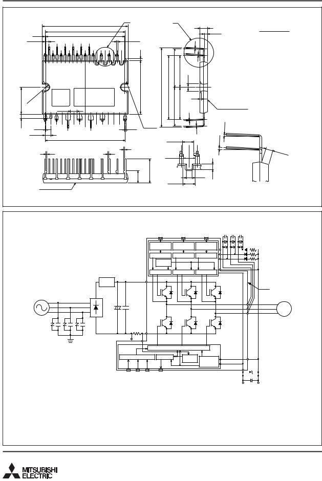
Fig. 1 PACKAGE OUTLINES (PS21965-4) |
Dimensions in mm |
A |
B |
38±0.5 |
|
0.28
1.778 ±0.2
17
|
|
.6 |
|
12 |
-R1 |
|
|
2 |
|
||
|
|
|
|
20×1.778(=35.56)
35±0.3
QR |
Type name |
Code |
Lot No. |
3 MIN |
|
16-0.5
1 |
(1) |
24±0.5
18 |
25 |
|
0.28 |
8-0.6 |
4-C1.2 |
|
||
2.54 ±0.2 |
|
|
14×2.54(=35.56) |
|
|
0.5 |
0.5 |
|
0.5 |
0.5 |
|
|
5.5±0.5 |
9.5±0.5 |
HEAT SINK SIDE |
|
|
3.5
4 . 0
0.5 |
14.4±0.5 |
(3.5) |
29.2± |
|
|
|
14.4±0.5 |
0.8 |
|
|
0 . 4
2.5 MIN
(2.656)
(1.2)
(2.756)
DETAIL A
1.5 ±0.05
(3.3)
HEAT SINK SIDE
) ° (0~5
(1.2)
TERMINAL CODE
1.NC
2.VUFB
3.VVFB
4.VWFB
5.UP
6.VP
7.WP
8.VP1
9.VNC *
10.UN
11.VN
12.WN
13.VN1
14.FO
15.CIN
16.VNC *
17.NC
18.NC
19.NC
20.N
21.W
22.V
23.U
24.P
25.NC
1.5 |
MIN |
|
DETAIL B
*) Two VNC terminals (9 & 16 pin) are connected inside DIP-IPM, please connect either one to the 15V power supply GND outside and leave another one open.
Aug. 2007

MITSUBISHI SEMICONDUCTOR <Dual-In-Line Package Intelligent Power Module>
PS21965-4/-4A/-4C/-4W
TRANSFER-MOLD TYPE
INSULATED TYPE
Fig. 2 LONG TERMINAL TYPE PACKAGE OUTLINES (PS21965-4A)
0.28
1.778±0.2
17
|
|
.6 |
|
12 |
1 |
|
|
-R |
|
||
2 |
|
||
|
|
|
|
18
0.28
2.54±0.2
38±0.5
20×1.778(=35.56)
35±0.3
QR |
Type name |
Code |
Lot No. |
3 MIN |
|
A |
|
|
|
|
B |
|
|
|
|
|
|
|
3.5 |
16-0.5 |
|
|
|
|
1.5±0.05 |
|
|
|
|
|
4 |
|
|
|
|
|
|
. |
|
|
|
(1) |
|
|
0 |
|
|
1 |
|
|
|
|
|
|
|
|
|
|
|
|
|
|
|
|
|
±0.5 |
|
|
|
24±0.5 |
|
29.4±0.5 |
14.4 |
(3.5) |
(3.3) |
|
|
|
|
±0.5 |
|
0.8 |
|
|
|
|
|
|
|
|
|
|
|
14.4 |
|
HEAT SINK SIDE |
25 |
|
4-C1.2 |
|
|
|
|
|
|
|
. |
|
|
|
8-0.6 |
|
|
0 |
|
|
|
|
|
4 |
|
|
||
Dimensions in mm
TERMINAL CODE
1.NC
2.VUFB
3.VVFB
4.VWFB
5.UP
6.VP
7.WP
8.VP1
9.VNC *
10.UN
11.VN
12.WN
13.VN1
14.FO
15.CIN
16.VNC *
17.NC
18.NC
19.NC
20.N
21.W
22.V
23.U
24.P
25.NC
14×2.54(=35.56) |
|
|
0.5 |
0.5 |
2.5 MIN |
|
||
0.5 |
0.5 |
|
|
|
(2.656) |
|
±0.5 |
14±0.5 |
|
(1.2) |
|
|
5.5 |
(2.756) |
|
|
HEAT SINK SIDE
DETAIL A
(1.2)
) ° (0~5
1.5 |
MIN |
|
DETAIL B
*) Two VNC terminals (9 & 16 pin) are connected inside DIP-IPM, please connect either one to the 15V power supply GND outside and leave another one open.
Fig. 3 ZIGZAG TERMINAL TYPE PACKAGE OUTLINES (PS21965-4C) |
Dimensions in mm |
12
0.28
1.778±0.2
17
.6 -R1 2
38±0.5
20×1.778(=35.56)
35±0.3
QR |
Type name |
Code |
Lot No. |
3 MIN |
|
A |
|
|
|
|
B |
|
|
|
|
|
|
|
3.5 |
16-0.5 |
|
|
|
|
4 |
|
|
|
|
|
|
|
. |
|
|
|
|
|
|
0 |
|
|
|
|
|
|
4 |
1 |
(1) |
|
|
|
|
. |
|
|
|
|
0 |
||
|
|
|
|
|
|
|
|
24±0.5 |
33.7±0.5 |
29.2±0.5 |
18.9±0.5 |
14.4±0.5 |
(3.5) |
|
|
|
|
|
14.4±0.5 |
0.8 |
|
|
|
|
|
|
|
18 |
25 |
|
0 |
|
|
4-C1.2 |
|
|
|
4 |
|
0.28 |
8-0.6 |
|
. |
|
|
||
2.54±0.2 |
|
|
|
|
14×2.54(=35.56) |
|
|
|
0.5 |
|
|
0.5 |
0.5 |
|
(2.656) |
|
5.5±0.5 |
0.5 |
|
|
9.5± |
(1.2) |
|
|
|
|
(2.756)
HEAT SINK SIDE
DETAIL A
|
TERMINAL CODE |
|||
1.5±0.05 |
|
1. |
NC |
|
|
2. |
VUFB |
|
|
|
3. |
VVFB |
|
|
|
4. |
VWFB |
|
|
|
5. |
UP |
|
|
|
6. |
VP |
|
|
|
7. |
WP |
|
|
|
8. |
VP1 |
|
|
|
9. |
VNC * |
|
|
|
10. |
UN |
|
|
|
11. |
VN |
|
|
|
12. |
WN |
|
|
|
13. |
VN1 |
|
|
|
14. |
FO |
|
|
|
15. |
CIN |
|
|
|
16. |
VNC * |
|
|
|
17. |
NC |
|
|
|
18. |
NC |
|
|
|
19. |
NC |
|
|
HEAT SINK SIDE |
20. |
N |
|
|
|
21. |
W |
|
|
|
22. |
V |
|
|
) |
23. |
U |
|
|
° |
24. |
P |
|
|
(0~5 |
|
|||
25. |
NC |
|
||
) |
|
|
|
|
° |
|
|
|
|
(0~5 |
|
|
|
|
|
|
|
1.5 |
MIN |
|
|
|
|
|
(1.2) |
|
|
|
|
|
DETAIL B |
|
|
|
*) Two VNC terminals (9 & 16 pin) are connected inside DIP-IPM, please connect either one to the 15V power supply GND outside and leave another one open.
Aug. 2007
2
MITSUBISHI SEMICONDUCTOR <Dual-In-Line Package Intelligent Power Module>
PS21965-4/-4A/-4C/-4W
TRANSFER-MOLD TYPE
INSULATED TYPE
Fig. 4 BOTH SIDES ZIGZAG TERMINAL TYPE PACKAGE OUTLINES (PS21965-4W)
|
|
|
A |
|
|
|
|
B |
|
|
|
|
|
38±0.5 |
|
|
|
|
|
|
3.5 |
|
|
|
20×1.778(=35.56) |
|
|
|
|
|
|
|
|
|
|
|
|
|
|
|
|
1.5±0.05 |
|
|
0.28 |
|
35±0.3 |
|
|
|
|
|
|
|
|
|
|
|
|
|
|
|
|
||
|
1.778±0.25 |
|
16-0.5 |
|
|
|
|
4 |
|
|
|
|
|
|
|
|
|
|
|
. |
|
|
|
|
|
|
|
|
|
|
0 |
|
|
17 |
|
1 |
(1) |
|
|
|
|
|
|
|
|
|
|
|
|
|
4 |
|
||
|
|
|
|
|
|
|
|
|
|
|
|
|
|
|
|
|
|
|
|
. |
|
|
|
|
|
|
|
|
17.4±0.5 |
|
0 |
|
|
|
|
|
0.5 |
±0.6 |
±0.5 |
14.4±0.5 |
(3.5) |
|
|
|
|
QR |
Type name |
24± |
35.2 |
29.2 |
|
|
|
|
|
.6 |
|
|
|
|
|
0.8 |
|
||
12 |
-R1 |
Code |
Lot No. |
|
|
|
17.4±0.5 |
14.4±0.5 |
|
|
2 |
|
|
|
|
HEAT SINK SIDE |
|||||
|
|
|
|
|
|
|
||||
|
|
3 MIN |
|
|
|
|
|
|
|
|
|
|
|
|
|
|
|
|
|
|
|
|
|
|
|
|
|
|
|
|
0 |
|
|
|
|
|
|
|
|
|
|
. |
|
(1.8) |
|
|
|
|
4-C1.2 |
|
|
|
4 |
|
18 |
|
25 |
|
|
|
|
|
° |
||
|
|
|
|
|
|
|
|
|
|
) |
|
0.28 |
|
7-0.6 |
|
|
|
|
. |
(0~5 |
|
|
2.54 ±0.25 |
|
|
|
|
|
|
|
0 |
|
|
|
|
|
|
|
|
|
4 |
|
|
|
14×2.54(=35.56) |
|
|
|
) |
|
|
|
|
° |
|
|
|
2.5 MIN |
|
(0~5 |
|
|
|
|
|
||
|
|
|
|
|
|
|
0.5 |
|
|
|
|
0.5 |
0.5 |
|
(2.656) |
|
|
|
|
|
|
|
|
|
5.5±0.5 |
±0.5 |
|
|
(1.2) |
|
11 |
|
(1.2) |
||
|
|
|
|
|
|
|
|
|
(2.756) |
|
|
HEAT SINK SIDE
DETAIL A
Dimensions in mm
TERMINAL CODE
1.NC
2.VUFB
3.VVFB
4.VWFB
5.UP
6.VP
7.WP
8.VP1
9.VNC *
10.UN
11.VN
12.WN
13.VN1
14.FO
15.CIN
16.VNC *
17.NC
18.NC
19.NC
20.N
21.W
22.V
23.U
24.P
25.NC
1.5 |
MIN |
|
DETAIL B
*) Two VNC terminals (9 & 16 pin) are connected inside DIP-IPM, please connect either one to the 15V power supply GND outside and leave another one open.
Fig. 5 INTERNAL FUNCTIONS BLOCK DIAGRAM (TYPICAL APPLICATION EXAMPLE)
C1 : Electrolytic type with good temperature and frequency |
High-side input (PWM) |
|
|
|
–CBU |
–CBV CBU+ |
–CBW CBV+ |
CBW+ |
|||||||||
(3V, 5V line)(Note 1, 2) |
|
|
|
|
|
|
|
|
|
|
|
||||||
characteristics |
|
|
|
|
|
|
|
|
|
|
|
|
C2 |
||||
|
|
|
|
|
|
|
|
|
|
|
|
||||||
(Note : The capacitance value depends on the PWM control |
Input signal |
Input signal |
Input signal |
|
|
C1 |
|||||||||||
scheme used in the applied system). |
|
|
(Note 6) |
||||||||||||||
conditioning |
conditioning |
conditioning |
|
|
|
||||||||||||
C2 : 0.22~2µF R-category ceramic capacitor for noise filtering. |
Level shifter |
Level shifter |
Level shifter |
|
|
|
|
|
|
|
(Note 5) |
||||||
|
|
|
|
|
|
||||||||||||
|
|
|
|
|
|
|
|||||||||||
|
Protection |
|
|
|
|
|
|
|
|
|
|
|
|
|
|||
|
|
|
|
|
|
|
|
|
|
|
|
|
|
|
|||
|
circuit (UV) |
|
|
|
|
|
|
|
|
|
|
|
|
|
|
||
|
|
Inrush current |
Drive circuit |
Drive circuit Drive circuit |
|
|
|
limiter circuit |
|
||
|
|
|
|
|
|
|
|
P |
|
H-side IGBTS |
|
|
|
|
|
|
|
|
|
|
|
|
DIP-IPM |
AC line input |
|
|
|
|
|
|
|
|
|
U |
|
|
|
(Note 4) |
|
V |
M |
|
|
|
|
W |
|
|
|
|
|
|
(Note 7) |
|
|
|
|
|
AC line output |
Z |
C |
N1 |
N |
|
|
|
|
|
|
||
L-side IGBTS
|
VNC |
|
|
|
|
Z : ZNR (Surge absorber) |
CIN |
|
|
|
|
|
Drive circuit |
|
|||
C : AC filter (Ceramic capacitor 2.2~6.5nF) |
|
|
|||
|
|
|
|
||
(Note : Additionally, an appropriate line-to line |
Input signal conditioning |
Fo logic |
Protection |
Control supply |
|
surge absorber circuit may become necessary |
|||||
|
|
circuit |
Under-Voltage |
||
depending on the application environment). |
|
|
|
||
|
|
|
protection |
||
|
|
|
|
|
|
|
|
|
|
|
|
|
|
|
|
(Note 6) |
Low-side input (PWM) FO |
|
|
|
|
|
|
||||||||||
|
|
|
|
|
|
|||||||||||
(3V, 5V line)(Note 1, 2) |
Fault output (5V line) |
|
|
|
|
|
|
|
||||||||
|
|
|
|
|
|
|
|
|
|
|
|
|
|
|||
|
|
|
|
|
|
|
(Note 3) |
VNC |
|
|
|
|
|
VD |
||
|
|
|
|
|
|
|
|
|
|
|
(15V line) |
|||||
Note1: Input logic is high-active. There is a 3.3kΩ (min) pull-down resistor built-in each input circuit. When using an external CR filter, please make it satisfy the input threshold voltage.
2:By virtue of integrating an application specific type HVIC inside the module, direct coupling to MCU terminals without any opto-coupler or transformer isolation is possible. (see also Fig. 11)
3:This output is open drain type. The signal line should be pulled up to the positive side of the 5V power supply with approximately 10kΩ resistor. (see also Fig. 11)
4:The wiring between the power DC link capacitor and the P, N1 terminals should be as short as possible to protect the DIP-IPM against catastrophic high surge voltages. For extra precaution, a small film type snubber capacitor (0.1~0.22µF, high voltage type) is recommended to be mounted close to these P & N1 DC power input pins.
5:High voltage (600V or more) and fast recovery type (less than 100ns) diodes should be used in the bootstrap circuit.
6:It is recommended to insert a Zener diode (24V/1W) between each pair of control supply terminals to prevent surge destruction.
7:Bootstrap negative electrodes should be connected to U, V, W terminals directly and separated from the main output wires.
Aug. 2007
3
 Loading...