


 Loading...
Mitsubishi M37905M8C-XXXSP, M37905M8C-XXXFP, M37905M6C-XXXSP, M37905M6C-XXXFP, M37905M4C-XXXSP Datasheet
...
|
|
|
|
|
|
Y |
|
PRELIMINAR |
|
||||||
|
|
|
|
|
|
. . |
|
|
|
|
|
|
specification |
change |
|
|
|
|
|
|
|
to |
|
|
|
|
a |
final |
|
subject |
|
|
is |
not |
are |
|
|
||
|
limits |
|
|
|
|||
This |
|
|
|
|
|||
|
|
|
|
|
|||
|
|
|
|
|
|
|
|
Notice:parametric |
|
|
|
|
|
||
Some |
|
|
|
|
|
|
|
MITSUBISHI MICROCOMPUTERS
M37905M4C-XXXFP, M37905M4C-XXXSP M37905M6C-XXXFP, M37905M6C-XXXSP M37905M8C-XXXFP, M37905M8C-XXXSP
16-BIT CMOS MICROCOMPUTER
DESCRIPTION
These are single-chip 16-bit microcomputers designed with high-per- formance CMOS silicon gate technology, being packaged in 64-pin plastic molded QFP or shrink plastic molded SDIP. These microcomputers support the 7900 Series instruction set, which are enhanced and expanded instruction set and are upper-compatible with the
7700/7751 Series instruction set.
The CPU of these microcomputers is a 16-bit parallel processor that can also be switched to perform 8-bit parallel processing. Also, the bus interface unit of these microcomputers enhances the memory access efficiency to execute instructions fast. Therefore, these microcomputers are suitable for office, business, and industrial equipment controller that require high-speed processing of large data.
Also, they are suitable for motor-control equipment since each of them includes the motor control circuit.
[M37905M8C-XXXFP, M37905M8C-XXXSP] |
|
|
ROM .............................................................................. |
|
60 Kbytes |
RAM ............................................................................. |
|
3072 bytes |
• Instruction execution time |
|
|
The fastest instruction at 20 MHz frequency ........................ |
50 ns |
|
• Single power supply .................................................... |
5 V ± 0.5 V |
|
• Interrupts ........... |
8 external sources, 23 internal sources, 7 levels |
|
• Multi-functional 16-bit timer ................................................. |
10 + 3 |
|
(Three-phase motor drive waveform and Pulse motor drive waveform output are available.)
• Serial I/O (UART or Clock synchronous) |
..................................... 3 |
• 10-bit A-D converter .......................................... |
12-channel inputs |
• 8-bit D-A converter ............................................ |
2-channel outputs |
• 12-bit watchdog timer |
|
• Programmable input/output (ports P1, P2, P4, P5, P6, P7, P8) .. 50
DISTINCTIVE FEATURES |
|
APPLICATION |
• Number of basic machine instructions .................................... |
203 |
Control devices for office equipment such as copiers and facsimiles |
• Memory |
|
Control devices for industrial equipment such as communication |
[M37905M4C-XXXFP, M37905M4C-XXXSP] |
|
and measuring instruments |
ROM .............................................................................. |
32 Kbytes |
Control devices for equipment, requiring motor control, such as |
RAM ............................................................................. |
1024 bytes |
inverter air conditioners and general-purpose inverters |
[M37905M6C-XXXFP, M37905M6C-XXXSP] |
|
|
ROM .............................................................................. |
48 Kbytes |
|
RAM ............................................................................. |
3072 bytes |
|
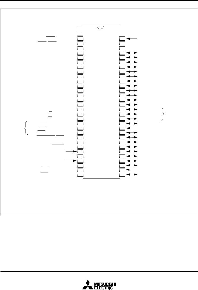
M37905MxC-XXXFP PIN CONFIGURATION (TOP VIEW)
|
|
|
|
|
|
|
|
|
|
|
|
|
|
|
|
P13/TxD0 |
|
P14/CTS1/RTS1 |
|
P15/CTS1/CLK1 |
P16/RxD1 |
P17/TxD1 |
P20/TA4OUT |
P21/TA4IN |
P22/TA9OUT |
P23/TA9IN |
|
P24(/TB0IN) |
|
P25(/TB1IN) Note |
|
P26(/TB2IN) |
|
P27 |
|
MD1 |
|
P40/TA5OUT/RTP20 |
|
P41/TA5IN/RTP21 |
|||||||||||
|
|
|
|
|
|
|
|
|
|
|
|
|
|
|
|
|
|
|
|
|
|
|
|
||||||||||||||||||||||||||||
|
|
|
|
|
|
|
|
|
|
|
|
|
|
|
|
|
|
|
|
|
|
|
|
||||||||||||||||||||||||||||
|
|
|
|
|
|
|
|
|
|
|
|
|
|
|
|
|
|
|
|
|
|
|
|
|
|||||||||||||||||||||||||||
|
|
|
|
|
|
|
|
|
|
|
|
|
|
|
|
|
|
|
|
|
|
|
|
|
|||||||||||||||||||||||||||
|
|
|
|
|
|
|
|
|
|
|
|
|
|
|
|
|
|
|
|
|
|
|
|
|
|
|
|
|
|
|
|
|
|
|
|
|
|
|
|
|
|
|
|
|
|
|
|
||||
|
|
|
|
|
|
|
|
|
|
|
|
|
|
|
|
|
|
|
|
|
|
|
|
|
|
|
|
|
|
|
|
|
|
|
|
|
|
|
|
|
|
|
|
|
|
|
|
|
|
|
|
|
|
|
|
|
|
|
|
|
|
|
|
|
|
|
|
|
|
|
|
|
|
|
|
|
|
|
|
|
|
|
|
|
|
|
|
|
|
|
|
|
|
|
|
|
|
|
|
|
|
|
|
|
|
|
|
|
|
|
|
|
|
|
|
|
|
|
48 |
47 |
46 |
45 |
44 |
43 |
42 |
41 |
40 |
39 |
38 |
37 |
36 |
35 |
|
34 |
|
33 |
|||||||||||||||||||
|
|
|
|
|
|
P12/RXD0 |
|
|
|
49 |
|
|
|
|
|
|
|
|
|
|
|
|
|
|
|
|
|
|
|
|
|
|
|
|
|
|
|
|
|
|
|
|
|
|
|
|
|
||||
|
|
|
|
|
|
|
|
|
|
|
|
|
|
|
|
|
|
|
|
|
|
|
|
|
|
|
|
|
|
|
|
|
|
|
|
|
|
|
|
|
|
|
|
|
|
||||||
|
P11 |
|
|
|
|
/CLK0 |
|
|
|
|
|
|
|
|
|
|
|
|
|
|
|
|
|
|
|
|
|
|
|
|
|
|
|
|
|
|
|
|
|
|
|
|
|
|
|
|
|
||||
|
/CTS0 |
|
|
|
50 |
|
|
|
|
|
|
|
|
|
|
|
|
|
|
|
|
|
|
|
|
|
|
|
|
|
|
|
|
|
|
|
|
|
|
|
|
|
|||||||||
|
P10 |
|
|
|
|
|
|
|
|
|
|
|
|
|
|
|
|
|
|
|
|
|
|
|
|
|
|
|
|
|
|
|
|
|
|
|
|
|
|
|
|
|
|
|
|
|
|
|
|
|
|
|
/CTS0 |
|
/RTS0 |
|
|
|
|
51 |
|
|
|
|
|
|
|
|
|
|
|
|
|
|
|
|
|
|
|
|
|
|
|
|
|
|
|
|
|
|
|
|
|
|
|
|
|
||||||
|
|
|
|
|
|
|
|
|
VCC |
|
|
|
|
|
|
|
|
|
|
|
|
|
|
|
|
|
|
|
|
|
|
|
|
|
|
|
|
|
|
|
|
|
|
|
|
|
|
|
|
|
|
|
|
|
52 |
|
|
|
|
|
|
|
|
|
|
|
|
|
|
|
|
|
|
|
|
|
|
|
|
|
|
|
|
|
|
|
|
|
|
|
|
|
|||||||||||
|
|
|
|
|
|
|
|
AVCC |
|
|
|
53 |
|
|
|
|
|
|
|
|
|
|
|
|
|
|
|
|
|
|
|
|
|
|
|
|
|
|
|
|
|
|
|
|
|
|
|
|
|
||
|
|
|
|
|
|
|
|
VREF |
|
|
|
54 |
|
|
|
|
|
|
|
|
|
|
|
|
|
|
|
|
|
|
|
|
|
|
|
|
|
|
|
|
|
|
|
|
|
|
|
|
|
||
|
|
|
|
|
|
|
|
|
|
|
|
|
|
|
|
|
|
|
|
|
|
|
|
|
|
|
|
|
|
|
|
|
|
|
|
|
|
|
|
|
|
|
|
|
|
|
|
||||
|
|
|
|
|
|
|
|
AVSS |
|
|
|
|
|
|
|
|
|
|
|
|
|
|
|
|
|
|
|
|
|
|
|
|
|
|
|
|
|
|
|
|
|
|
|
|
|
|
|
|
|
||
|
|
|
55 |
|
|
|
|
|
|
|
|
|
|
|
|
|
|
|
|
|
|
|
|
|
|
|
|
|
|
|
|
|
|
|
|
|
|
|
|
|
|||||||||||
|
|
|
|
|
|
|
|
|
|
|
|
|
|
|
|
|
|
|
|
M37905MXC-XXXFP |
|
|
|
|
|
|
|||||||||||||||||||||||||
|
|
|
|
|
|
|
|
|
VSS |
|
|
|
56 |
|
|
|
|
|
|
|
|
|
|
|
|||||||||||||||||||||||||||
|
|
|
|
|
|
|
|
|
|
|
|
|
|
|
|||||||||||||||||||||||||||||||||||||
|
P83/AN11/TXD2 |
|
|
|
57 |
|
|
|
|
|
|
|
|
|
|
|
|
|
|
|
|
|
|
|
|
|
|
|
|
|
|
|
|
|
|
|
|
|
|
|
|
|
|||||||||
|
P82/AN10/RXD2 |
|
|
|
|
|
|
|
|
|
|
|
|
|
|
|
|
|
|
|
|
|
|
|
|
|
|
|
|
|
|
|
|
|
|
|
|
|
|
|
|
|
|||||||||
|
|
|
|
58 |
|
|
|
|
|
|
|
|
|
|
|
|
|
|
|
|
|
|
|
|
|
|
|
|
|
|
|
|
|
|
|
|
|
|
|
|
|
||||||||||
P81/AN9 |
/CTS2 |
/CLK2 |
|
|
|
59 |
|
|
|
|
|
|
|
|
|
|
|
|
|
|
|
|
|
|
|
|
|
|
|
|
|
|
|
|
|
|
|
|
|
|
|
|
|
||||||||
|
|
|
|
|
|
|
|
|
|
|
|
|
|
|
|
|
|
|
|
|
|
|
|
|
|
|
|
|
|
|
|
|
|
|
|
|
|
|
|
||||||||||||
P80/AN8 |
/CTS2 |
|
/RTS2 |
/DA1 |
|
|
|
60 |
|
|
|
|
|
|
|
|
|
|
|
|
|
|
|
|
|
|
|
|
|
|
|
|
|
|
|
|
|
|
|
|
|
|
|
|
|
||||||
|
|
|
|
|
|
|
|
|
|
|
|
|
|
|
|
|
|
|
|
|
|
|
|
|
|
|
|
|
|
|
|
|
|
|
|
|
|
|
|
|
|||||||||||
|
P77/AN7/DA0 |
|
|
|
|
|
|
|
|
|
|
|
|
|
|
|
|
|
|
|
|
|
|
|
|
|
|
|
|
|
|
|
|
|
|
|
|
|
|
|
|
|
|||||||||
|
|
|
|
61 |
|
|
|
|
|
|
|
|
|
|
|
|
|
|
|
|
|
|
|
|
|
|
|
|
|
|
|
|
|
|
|
|
|
|
|
|
|
||||||||||
|
|
|
|
|
|
P76/AN6 |
|
|
|
|
|
|
|
|
|
|
|
|
|
|
|
|
|
|
|
|
|
|
|
|
|
|
|
|
|
|
|
|
|
|
|
|
|
|
|
|
|
||||
|
|
|
|
|
|
|
|
|
62 |
|
|
|
|
|
|
|
|
|
|
|
|
|
|
|
|
|
|
|
|
|
|
|
|
|
|
|
|
|
|
|
|
|
|
|
|
|
|||||
|
|
|
|
|
|
P75/AN5 |
|
|
|
|
|
|
|
|
|
|
|
|
|
|
|
|
|
|
|
|
|
|
|
|
|
|
|
|
|
|
|
|
|
|
|
|
|
|
|
|
|
||||
|
|
|
|
|
|
|
|
|
63 |
|
|
|
|
|
|
|
|
|
|
|
|
|
|
|
|
|
|
|
|
|
|
|
|
|
|
|
|
|
|
|
|
|
|
|
|
|
|||||
|
|
|
|
|
|
P74/AN4 |
|
|
|
|
|
|
|
|
|
|
|
|
|
|
|
|
|
|
|
|
|
|
|
|
|
|
|
|
|
|
|
|
|
|
|
|
|
|
|
|
|
||||
|
|
|
|
|
|
|
|
|
64 |
|
|
|
|
|
|
|
|
|
|
|
|
|
|
|
|
|
|
|
|
|
|
|
|
|
|
|
|
|
|
|
|
|
|
|
|
|
|||||
|
|
|
|
|
|
|
|
|
|
|
|
|
|
|
|
|
|
|
|
|
|
|
|
|
|
|
|
|
|
|
|
|
|
|
|
|
|
|
|
|
|
|
|
|
|
|
|
|
|
|
|
|
|
|
|
|
|
|
|
|
|
|
|
|
|
|
|
1 |
2 |
3 |
4 |
5 |
6 |
7 |
8 |
9 |
10 |
11 |
12 |
13 |
14 |
|
15 |
|
16 |
||||||||||||||||||
|
|
|
|
|
|
|
|
|
|
|
|
|
|
|
|
|
|
|
|
|
|
|
|
|
|
|
|
|
|
|
|
|
|
|
|
|
|
|
|
|
|
|
|
|
|
|
|
|
|
|
|
|
|
|
|
|
|
|
|
|
|
|
|
|
|
|
|
|
|
|
|
|
|
|
|
|
|
|
|
|
|
|
|
|
|
|
|
|
|
|
|
|
|
|
|
|
|
|
|
|
|
|
|
|
|
|
|
|
|
|
|
|
|
|
|
|
|
|
|
P73/AN3 |
|
P72/AN2 |
|
P71/AN1 |
P70/AN0 |
P67/TA3IN/RTP13 |
P66/TA3OUT/RTP12 |
P65/TA2IN/U/RTP11 |
P64/TA2OUT/V/RTP10 |
P63/TA1IN/W/RTP03 |
|
P62/TA1OUT/U/RTP02 |
|
P61/TA0IN/V/RTP01 |
|
P60/TA0OUT/W/RTP00 |
|
P57/INT7/TB2IN/IDU |
|
P56/INT6/TB1IN/IDV |
|
P55/INT5/TB0IN/IDW |
|
P6OUTCUT/INT4 |
|||||||||||
|
|
|
|
|
|
|
|
|
|
|
|
|
|
|
|
|
|
|
|
|
|
|
|
|
|||||||||||||||||||||||||||
|
|
|
|
|
|
|
|
|
|
|
|
|
|
|
|
|
|
|
|
|
|
|
|
|
|||||||||||||||||||||||||||
|
|
|
|
|
|
|
|
|
|
|
|
|
|
|
|
|
|
|
|
|
|
|
|
|
|||||||||||||||||||||||||||
|
|
|
|
|
|
|
|
|
|
|
|
|
|
|
|
|
|
|
|
|
|
|
|||||||||||||||||||||||||||||
|
|
|
|
|
|
|
|
|
|
|
|
|
|
|
|
|
|
|
|
|
|
|
|
|
|
|
|
|
|
|
|||||||||||||||||||||
|
|
|
|
|
|
|
|
|
|
|
|
|
|
|
|
|
|
|
|
|
|
|
|
|
|
|
|
||||||||||||||||||||||||
|
|
|
|
|
|
|
|
|
|
|
|
|
|
|
|
|
|
|
|
|
|
|
|
|
|
|
|
|
|
|
|||||||||||||||||||||
|
|
|
|
|
|
|
|
|
|
|
Outline 64P6N-A |
|
|
|
|
|
|
|
|
|
|
Note |
|
|
|
|
|
|
|||||||||||||||||||||||
|
|
|
|
|
|
|
|
|
|
|
|
|
|
|
|
|
|
|
|
|
|
|
|
|
|
|
|
|
|||||||||||||||||||||||
|
|
|
|
|
|
|
|
|
|
|
|
|
|
|
|
|
|
|
|
|
|
|
|
|
|
|
|
|
|
|
|
|
|
|
|
|
|
|
|
|
|
|
|
|
|
|
|
|
|
|
|
|
|
|
|
|
|
|
|
|
|
|
|
|
|
|
|
|
|
|
|
|
|
|
|
|
|
|
|
|
|
|
|
|
|
|
|
|
|
|
|
|
|
|
|
|
|
|
|
|
|
|
|
|
|
|
|
|
|
|
|
|
|
|
|
|
|
|
|
|
|
|
|
|
|
|
|
|
|
|
|
|
|
|
|
|
|
|
|
|
|
|
|
|
|
|
|
|
|
|
|
|
|
|
|
|
|
|
|
|
|
|
|
|
|
|
|
|
|
|
|
|
|
|
|
|
|
|
|
|
|
|
|
|
|
|
|
|
|
|
|
|
|
|
|
|
|
|
|
|
|
|
|
|
|
|
|
32 |
|
|
|
|
|
|
P42/TA6OUT/RTP22 |
|||||||||||||
|
|
|
||||||||||||||||||
31 |
|
|
|
|
|
|
P43/TA6IN/RTP23 |
|||||||||||||
|
|
|
||||||||||||||||||
30 |
|
|
|
|
|
|
P44/TA7OUT/RTP30 |
|||||||||||||
|
|
|
||||||||||||||||||
29 |
|
|
|
|
|
|
P45/TA7IN/RTP31 |
|||||||||||||
|
|
|
||||||||||||||||||
28 |
|
|
|
|
|
|
P46/TA8OUT/RTP32 |
|||||||||||||
|
|
|
|
|
|
|||||||||||||||
|
|
|
|
|||||||||||||||||
27 |
|
|
|
|
|
|
P47/TA8IN/RTP33 |
|||||||||||||
|
|
|
|
|||||||||||||||||
26 |
|
|
|
|
|
|
|
P4OUTCUT |
|
/INT0 |
|
|||||||||
|
|
|
|
|
|
|||||||||||||||
25 |
|
|
|
|
|
|
P51 |
/INT1 |
|
|
|
|
||||||||
|
|
|
|
|
|
|
|
|
||||||||||||
24 |
|
|
|
|
|
|
P52 |
|
/INT2 |
/RTPTRG1 |
||||||||||
|
|
|
|
|
||||||||||||||||
23 |
|
|
|
|
|
|
P53 |
|
|
|
|
|
||||||||
/INT3/RTPTRG0 |
||||||||||||||||||||
|
|
|
|
|
||||||||||||||||
22 |
|
|
|
|
|
|
VSS |
|||||||||||||
|
|
|
|
|
|
|||||||||||||||
21 |
|
|
|
|
|
|
VCONT |
|||||||||||||
|
|
|
|
|
|
|||||||||||||||
20 |
|
|
|
|
|
|
XOUT |
|||||||||||||
|
|
|
|
|
|
|||||||||||||||
19 |
|
|
|
|
|
|
XIN |
|||||||||||||
|
|
|
|
|
|
|||||||||||||||
18 |
|
|
|
|
|
|
|
|
RESET |
|
|
|
|
|
|
|
||||
|
|
|
|
|
|
|
|
|
|
|
|
|
|
|
||||||
17 |
|
|
|
|
|
|
MD0 |
|||||||||||||
|
|
|
|
|
|
|||||||||||||||
|
|
|
|
|
|
|
|
|
|
|
|
|
|
|
|
|
|
|
|
|
Note : Allocation of pins TB0IN to TB2IN can be switched by software.
|
|
|
|
|
|
Y |
|
PRELIMINAR |
|
||||||
|
|
|
|
|
|
. . |
|
|
|
|
|
|
specification |
change |
|
|
|
|
|
|
|
to |
|
|
|
|
a |
final |
|
subject |
|
|
is |
not |
are |
|
|
||
|
limits |
|
|
|
|||
This |
|
|
|
|
|||
|
|
|
|
|
|||
|
|
|
|
|
|
|
|
Notice:parametric |
|
|
|
|
|
||
Some |
|
|
|
|
|
|
|
MITSUBISHI MICROCOMPUTERS
M37905M4C-XXXFP, M37905M4C-XXXSP M37905M6C-XXXFP, M37905M6C-XXXSP M37905M8C-XXXFP, M37905M8C-XXXSP
16-BIT CMOS MICROCOMPUTER
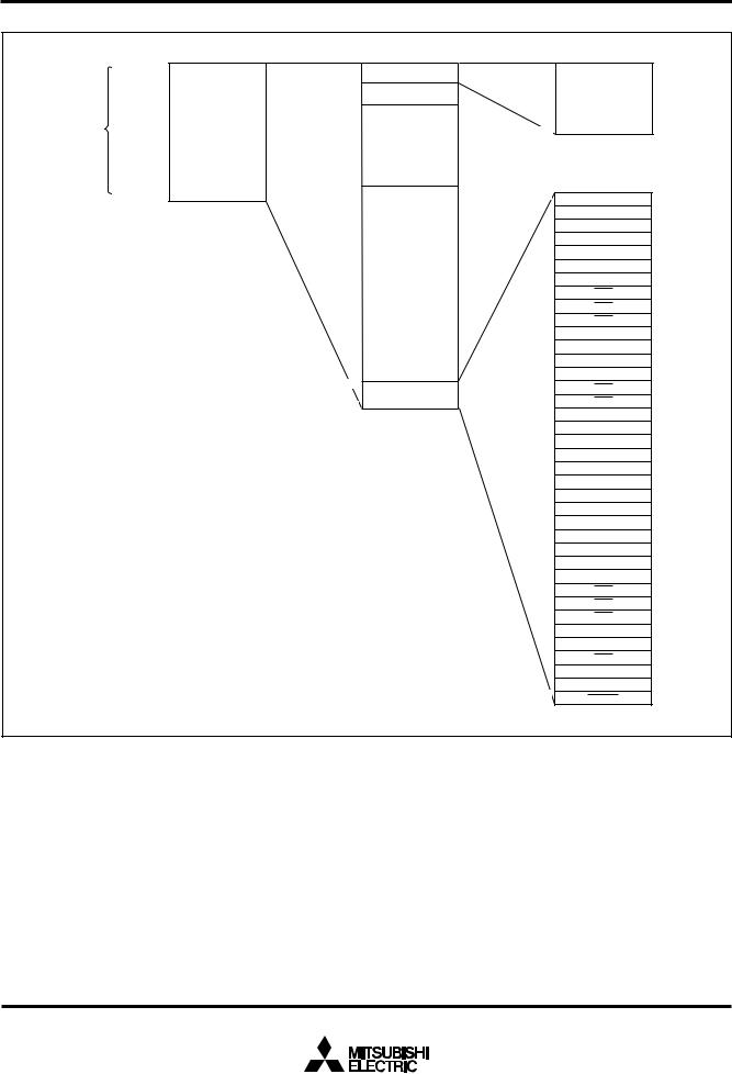
M37905MxC-XXXSP PIN CONFIGURATION (TOP VIEW)
P83/AN11/TxD2 


P82/AN10/RxD2 

P81/AN9/CTS2/CLK2 

P80/AN8/CTS2/RTS2/DA1 

P77/AN7/DA0 

P76/AN6 

P75/AN5 

P74/AN4 

P73/AN3 

P72/AN2 

P71/AN1 

P70/AN0 

P67/TA3IN/RTP13 

P66/TA3OUT/RTP12 

P65/TA2IN/U/RTP11 

P64/TA2OUT/V/RTP10 

P63/TA1IN/W/RTP03 

P62/TA1OUT/U/RTP02 

P61/TA0IN/V/RTP01 

P60/TA0OUT/W/RTP00 

P57/INT7/TB2IN/IDU 

Note P56/INT6/TB1IN/IDV 

P55/INT5/TB0IN/IDW 

P6OUTCUT/INT4 
MD0 
RESET 
XIN
XOUT 
VCONT
VSS
P53/INT3/RTPTRG0 

P52/INT2/RTPTRG1 

1 |
|
2 |
|
3 |
|
4 |
|
5 |
|
6 |
|
7 |
|
8 |
|
9 |
|
10 |
|
11 |
|
12 |
X-CM37905M |
19 |
|
13 |
|
14 |
|
15 |
|
16 |
|
17 |
|
18 |
XXXSP |
23 |
|
20 |
|
21 |
|
22 |
|
24 |
|
25 |
|
26 |
|
27 |
Outline 64P4B |
28 |
|
29 |
|
30 |
|
31 |
|
32 |
|
|
|
|
|
|
|
VSS |
|
|
|||||||||||||||||
64 |
|
|
|
|
|
|
|
||||||||||||||||||
|
|
|
|
|
|
AVSS |
|
|
|||||||||||||||||
63 |
|
|
|
|
|
|
|
||||||||||||||||||
62 |
|
|
|
|
|
VREF |
|
|
|||||||||||||||||
61 |
|
|
|
|
|
AVCC |
|
|
|||||||||||||||||
60 |
|
|
|
|
|
VCC |
|
|
|||||||||||||||||
59 |
|
|
|
|
|
P10 |
|
|
|
|
|
|
|
|
|
|
|
|
|
|
|
|
|
||
|
|
/CTS0 |
/RTS0 |
||||||||||||||||||||||
|
|
||||||||||||||||||||||||
58 |
|
|
|
|
|
P11 |
/CTS0 |
/CLK0 |
|
|
|||||||||||||||
|
|
|
|
||||||||||||||||||||||
57 |
|
|
|
|
|
P12/RxD0 |
|
|
|||||||||||||||||
56 |
|
|
|
|
|
P13/TxD0 |
|
|
|||||||||||||||||
55 |
|
|
|
|
|
P14 |
|
|
|
|
|
|
|
|
|
|
|
|
|
||||||
|
|
/CTS1 |
/RTS1 |
|
|
||||||||||||||||||||
54 |
|
|
|
|
|
P15 |
/CTS1 |
/CLK1 |
|
|
|||||||||||||||
53 |
|
|
|
|
|
P16/RxD1 |
|
|
|||||||||||||||||
52 |
|
|
|
|
|
P17/TxD1 |
|
|
|||||||||||||||||
51 |
|
|
|
|
|
P20/TA4OUT |
|
|
|||||||||||||||||
50 |
|
|
|
|
|
P21/TA4IN |
|
|
|||||||||||||||||
49 |
|
|
|
|
|
P22/TA9OUT |
|
|
|||||||||||||||||
48 |
|
|
|
|
|
P23/TA9IN |
|
|
|||||||||||||||||
47 |
|
|
|
|
|
P24(/TB0IN) |
|
|
Note |
||||||||||||||||
|
|
|
|
|
|
||||||||||||||||||||
46 |
|
|
|
|
|
P25(/TB1IN) |
|
|
|||||||||||||||||
|
|
||||||||||||||||||||||||
45 |
|
|
|
|
|
P26(/TB2IN) |
|
|
|
|
|||||||||||||||
|
|
|
|
|
|
|
|
||||||||||||||||||
44 |
|
|
|
|
|
P27 |
|
|
|||||||||||||||||
|
|
|
|
||||||||||||||||||||||
43 |
|
|
|
|
|
MD1 |
|
|
|||||||||||||||||
|
|
|
|
||||||||||||||||||||||
42 |
|
|
|
|
|
P40/TA5OUT/RTP20 |
|||||||||||||||||||
41 |
|
|
|
|
|
P41/TA5IN/RTP21 |
|||||||||||||||||||
40 |
|
|
|
|
|
P42/TA6OUT/RTP22 |
|||||||||||||||||||
39 |
|
|
|
|
|
P43/TA6IN/RTP23 |
|||||||||||||||||||
|
|
|
|||||||||||||||||||||||
38 |
|
|
|
|
|
P44/TA7OUT/RTP30 |
|||||||||||||||||||
|
|
|
|||||||||||||||||||||||
37 |
|
|
|
|
|
P45/TA7IN/RTP31 |
|||||||||||||||||||
36 |
|
|
|
|
|
P46/TA8OUT/RTP32 |
|||||||||||||||||||
|
|
|
|||||||||||||||||||||||
35 |
|
|
|
|
|
P47/TA8IN/RTP33 |
|||||||||||||||||||
|
|
|
|||||||||||||||||||||||
34 |
|
|
|
|
|
P4OUTCUT |
|
/INT0 |
|
||||||||||||||||
|
|
|
|||||||||||||||||||||||
33 |
|
|
|
|
|
P51 |
/INT1 |
|
|
|
|
|
|
|
|||||||||||
|
|
|
|
|
|
||||||||||||||||||||
|
|
|
|
|
|
|
|
|
|
|
|
|
|
|
|
|
|
|
|
|
|
|
|
|
|
Note : Allocation of pins TB0IN to TB2IN can be switched by software.
Outline 64P4B
2

|
|
|
|
|
|
Y |
|
PRELIMINAR |
|
||||||
|
|
|
|
|
|
. . |
|
|
|
|
|
|
specification |
change |
|
|
|
|
|
|
|
to |
|
|
|
|
a |
final |
|
subject |
|
|
is |
not |
are |
|
|
||
|
|
|
|
||||
|
limits |
|
|
|
|||
This |
|
|
|
|
|||
|
|
|
|
|
|||
|
|
|
|
|
|
|
|
Notice:parametric |
|
|
|
|
|
||
Some |
|
|
|
|
|
|
|
MITSUBISHI MICROCOMPUTERS
M37905M4C-XXXFP, M37905M4C-XXXSP M37905M6C-XXXFP, M37905M6C-XXXSP M37905M8C-XXXFP, M37905M8C-XXXSP
16-BIT CMOS MICROCOMPUTER
|
|
|
|
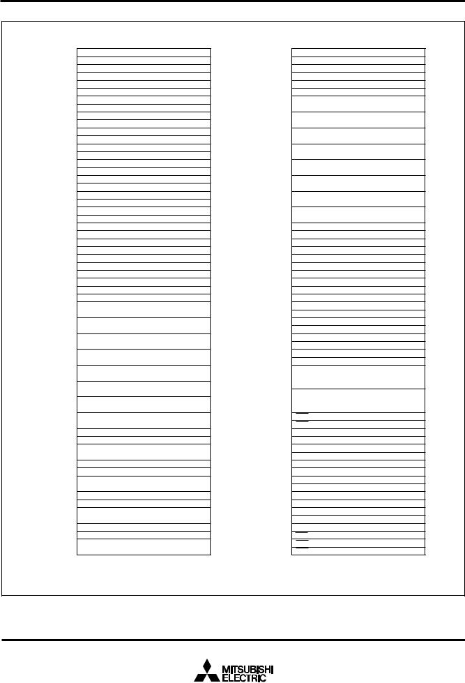
Data Buffer DQ0 |
(8) |
|
|
|
|
|
|
|
|
|
|
|
|
|
|
CUT |
|
Data Buffer DQ1 |
(8) |
|
|
|
|
|
|
|
|
|
|
|
|
|
|
|
|
|
|
|
|
|
|
|
|
|
|
|
|
|
|
|
|
P6OUT |
|
Data Buffer DQ2 |
(8) |
|
|
|
|
|
|
|
|
|
|
|
|
|
|
|
|
|
|
|
|
|
|
|
|
|
|
|
|
|
|
|
|
|
|
Data Buffer DQ3 |
(8) |
|
|
|
|
|
|
|
|
|
|
|
|
|
|
CUT |
|
Instruction Queue Buffer Q0 |
(8) |
|
|
|
|
|
|
|
|
|
|
|
|
|
|
P4OUT |
|
|
|
|
|
|
|
|
|
|
|
|
|||
|
|
|
Instruction Queue Buffer Q1 |
(8) |
|
|
|
|
|
|
|
|
|
|
|
||
|
|
|
|
Instruction Queue Buffer Q2 |
(8) |
|
|
|
|
|
|
|
|
|
|
|
|
Reference |
VoltageInput |
|
|
Instruction Queue Buffer Q3 |
(8) |
|
|
|
|
|
|
|
|
|
|
|
|
VREF |
|
Instruction Queue Buffer Q4 |
(8) |
|
|
|
|
|
|
|
|
|
|
|
|||
|
Instruction Queue Buffer Q5 |
(8) |
|
|
|
|
|
|
|
|
|
|
|
||||
|
|
|
|
|
|
|
|
|
|
|
|
|
|
|
|||
|
|
|
|
Instruction Queue Buffer Q6 |
(8) |
|
|
|
|
|
|
|
|
|
|
|
|
|
|
AVCC |
Register(8) |
Instruction Queue Buffer Q7 |
(8) |
|
|
|
|
|
|
|
|
|
|
|
|
|
|
Instruction Queue Buffer Q8 |
(8) |
|
|
|
|
|
|
|
|
|
|
|
|||
|
|
|
Instruction |
Instruction Queue Buffer Q9 |
(8) |
|
|
|
|
|
|
|
|
|
|
|
|
|
|
|
|
|
|
|
|
|
|
|
|
|
|
|
|
|
|
|
(0V) |
AVSS |
|
|
|
|
|
|
|
|
|
|
P1 |
|
|
|
|
|
|
|
|
Incrementer (24) |
|
|
|
|
|
|
P1(8) |
Input/Output |
|
|
|
|
|
|
|
|
|
Program Address Register PA (24) |
|
|
|
|
|
|
|
|
|
||||
|
|
|
|
|
|
|
|
|
|
|
|
|
|
|
|
||
|
|
MD1 |
|
Data Address Register DA (24) |
|
|
|
|
|
|
|
|
|
|
|
||
|
|
|
Incrementer/Decrementer (24) |
|
|
UART2(9) |
|
|
P2(8) |
Input/OutputP2 |
|
|
|
|
|||
|
|
|
|
|
|
|
|
|
|
|
|
|
|
||||
|
|
MD0 |
|
Program Counter PC (16) |
|
|
|
|
|
|
|
|
|
|
|
|
|
|
|
|
|
|
|
|
|
|
|
|
|
P4 |
|
|
|
|
|
|
|
|
|
Program Bank Register PG |
(8) |
|
|
|
|
|
|
|
|
|
|
||
|
|
|
|
|
|
|
|
|
|
Input/Output |
|
|
|
|
|||
|
|
|
|
Data Bank Register DT (8) |
|
|
|
|
|
|
P4(8) |
|
|
|
|
||
|
(0V) |
|
|
|
|
|
|
|
|
|
|
|
|
|
|
||
|
VSS |
|
Input Buffer Register IB (16) |
|
|
|
|
|
|
|
|
|
Kbytes 3Kbytes |
Kbytes 3Kbytes |
|||
|
|
|
|
Processor Status Register PS (11) |
TimerTA9(16) |
TimerTA8(16) |
TimerTA7(16) |
TimerTA6(16) |
TimerTA5(16) |
P5(6) |
Input/OutputP5 |
ROM RAM |
Kbytes 1Kbyte |
||||
|
|
VCC |
|
Direct Page Register DPR0 (16) |
|||||||||||||
|
|
|
Direct Page Register DPR1 (16) |
||||||||||||||
|
|
|
|
|
|
|
|
|
|
P6 |
|
32 |
48 |
60 |
|||
|
|
|
|
|
|
|
|
|
|
|
|
|
|
||||
|
|
|
|
Direct Page Register DPR2 (16) |
|
|
|
|
|
P8(4) P7(8) P6(8) |
Input/OutputP8 Input/OutputP7 Input/Output |
|
M37905M4C-XXXFP,M37905M4C-XXXSP |
M37905M6C-XXXFP,M37905M6C-XXXSP |
M37905M8C-XXXFP,M37905M8C-XXXSP |
||
|
Clockinput Clockoutput Resetinput |
XXRESETINOUT |
|
Direct Page Register DPR3 (16) |
|
|
|
|
|
|
|||||||
|
|
Stack Pointer S (16) |
|
|
|
|
|
|
|
||||||||
|
|
Index Register Y (16) |
|
|
|
|
|
|
|
||||||||
|
ClockGeneratingCircuit |
Index Register X (16) |
|
|
|
|
|
|
|
||||||||
DIAGRAM |
Accumulator B (16) |
|
|
|
|
|
|
|
|||||||||
Accumulator A (16) |
|
|
|
ROM |
(Note) |
|
|
||||||||||
Arithmetic Logic |
|
|
Central |
|
|
Note: |
|||||||||||
BLOCK |
|
|
|
|
|
|
|
|
|
|
|
|
|
|
|
||
|
VCONT |
|
Unit (16) |
|
|
|
|
|
|
|
|
|
|
|
|
||
|
|
|
|
|
|
|
|
|
|
|
|
|
|
|
|||
|
|
|
|
|
|
|
|
|
|
|
|
|
|
|
|
|
3 |

|
|
|
|
|
Y |
|
PRELIMINAR |
|
|||||
|
|
|
|
|
. . |
|
|
|
|
|
specification |
change |
|
|
|
|
|
|
to |
|
|
a |
final |
|
subject |
|
|
isnot |
its |
are |
|
|
||
|
|
|
||||
This |
lim |
|
|
|
|
|
etric |
|
|
|
|
|
|
Notice:param |
|
|
|
|
|
|
e |
|
|
|
|
|
|
Som |
|
|
|
|
|
|
MITSUBISHI MICROCOMPUTERS
M37905M4C-XXXFP, M37905M4C-XXXSP M37905M6C-XXXFP, M37905M6C-XXXSP M37905M8C-XXXFP, M37905M8C-XXXSP
16-BIT CMOS MICROCOMPUTER
FUNCTIONS
|
|
|
|
Parameter |
|
|
Functions |
||
|
|
|
|
|
|
|
|
|
|
Number of basic machine instructions |
203 |
|
|
||||||
|
|
|
|
|
|
|
|
|
|
Instruction execution time |
|
|
|
50 ns (the fastest instruction at f(fsys) = 20 MHz) |
|||||
External clock input frequency f(XIN) |
20 MHz (Max.) |
|
|
||||||
System clock frequency f(fsys) |
20 MHz (Max.) |
|
|
||||||
Memory size |
|
ROM |
(Note 1) |
|
|
||||
|
|
|
|
|
|
|
|
|
|
|
|
|
|
|
RAM |
(Note 1) |
|
|
|
|
|
|
|
|
|
|
|
|
|
Programmable input/output |
|
P1, P2, P4, P6, P7 |
8-bit 5 |
|
|
||||
ports |
|
|
|
|
|
|
|||
|
P5 |
6-bit 1 |
|
|
|||||
|
|
|
|
|
|
|
|
|
|
|
|
|
|
|
P8 |
4-bit 1 |
|
|
|
|
|
|
|
|
|
|
|
|
|
Multi-functional timers |
|
TA0–TA9 |
16-bit 10 |
|
|
||||
|
|
|
|
|
|
|
|
|
|
|
|
|
|
|
TB0–TB2 |
16-bit 3 |
|
|
|
|
|
|
|
|
|
|
|
|
|
Serial I/O |
|
UART0, UART1, and UART2 |
(UART or Clock synchronous serial I/O) 3 |
||||||
|
|
|
|
|
|
|
|
|
|
A-D converter |
|
|
|
10-bit successive approximation method 1 (12 channels) |
|||||
|
|
|
|
|
|
|
|
|
|
D-A converter |
|
|
|
8-bit 2 |
|
|
|||
|
|
|
|
|
|
|
|
|
|
Dead-time timer |
|
|
|
8-bit 3 |
|
|
|||
|
|
|
|
|
|
|
|
|
|
Watchdog timer |
|
|
|
12-bit 1 |
|
|
|||
|
|
|
|
|
|
|
|
|
|
Interrupts |
|
Maskable interrups |
8 external sources, 20 internal sources. Each interrupt can be set |
||||||
|
|
|
|
|
|
|
to a priority level within the range of 0–7 by software. |
||
|
|
|
|
|
|
|
|
|
|
|
|
|
|
|
Non-maskable interrups |
3 internal sources |
|
|
|
|
|
|
|
|
|
|
|
|
|
Clock generating circuit |
|
|
|
Incorporated (externally connected to a ceramic resonator or |
|||||
|
|
|
|
|
|
|
quartz-crystal resonator). |
||
|
|
|
|
|
|
|
|
|
|
PLL frequency multiplier |
|
|
|
The following multiplication ratios are available: 2, 3, 4. |
|||||
|
|
|
|
|
|
|
|
|
|
Power supply voltage |
|
|
|
5 V±0.5 V |
|
|
|||
|
|
|
|
|
|
|
|
|
|
Power dissipation |
|
|
|
125 mW (at f(fsys) = 20 MHz, Typ, ; the PLL frequency multiplier is inactive.) |
|||||
Ports’ input/output |
|
nput/Output withstand voltage |
5 V |
|
|
||||
characteristics |
|
utput current |
5 mA |
|
|
||||
Memory expansion |
|
|
|
Not available (single-chip mode only). |
|||||
Operating ambient temperature range |
–20 to 85 °C |
|
|
||||||
Device structure |
|
|
|
CMOS high-performance silicon gate process |
|||||
Package |
|
|
|
(Note 2) |
|
|
|||
|
|
|
|
|
|
|
|||
Notes 1: |
ROM |
|
|
M37905M4C-XXXFP, M37905M4C-XXXSP |
|
32 Kbytes |
|||
|
|
|
|
||||||
|
|
|
|
|
|
M37905M6C-XXXFP, M37905M6C-XXXSP |
|
48 Kbytes |
|
|
|
|
|
|
|
M37905M8C-XXXFP, M37905M8C-XXXSP |
|
60 Kbytes |
|
|
RAM |
|
|
M37905M4C-XXXFP, M37905M4C-XXXSP |
|
1024 bytes |
|||
|
|
|
|
|
|
M37905M6C-XXXFP, M37905M6C-XXXSP |
|
3072 bytes |
|
|
|
|
|
|
|
M37905M8C-XXXFP, M37905M8C-XXXSP |
|
3072 bytes |
|
2: |
|
|
|
|
|
|
|
|
|
Packages |
|
M37905M4C-XXXFP, M37905M6C-XXXFP, M37905M8C-XXXFP |
64-pin plastic molded QFP (64P6N-A) |
||||||
|
|
|
|
|
|
|
|
||
|
|
|
|
M37905M4C-XXXSP, M37905M6C-XXXSP, M37905M8C-XXXSP |
64-pin shrink plastic moldeds DIP (64P4B) |
||||
|
|
|
|
|
|
|
|
|
|
4

|
|
|
|
|
Y |
|
PRELIMINAR |
|
|||||
|
|
|
|
|
. . |
|
|
|
|
|
specification |
change |
|
|
|
|
|
|
to |
|
|
a |
final |
|
subject |
|
|
isnot |
its |
are |
|
|
||
|
|
|
||||
This |
lim |
|
|
|
|
|
etric |
|
|
|
|
|
|
Notice:param |
|
|
|
|
|
|
e |
|
|
|
|
|
|
Som |
|
|
|
|
|
|
MITSUBISHI MICROCOMPUTERS
M37905M4C-XXXFP, M37905M4C-XXXSP M37905M6C-XXXFP, M37905M6C-XXXSP M37905M8C-XXXFP, M37905M8C-XXXSP
16-BIT CMOS MICROCOMPUTER
PIN DESCRIPTION
|
Pin |
|
|
Name |
Input/ |
Functions |
||
|
|
|
Output |
|||||
|
|
|
|
|
|
|
|
|
|
Vcc, Vss |
|
Power supply input |
— |
Apply 5 V±0.5 V to Vcc, and 0 V to Vss. |
|||
|
|
|
|
|
|
|
|
|
|
MD0 |
|
MD0 |
Input |
Connect this pin to VSS. |
|||
|
|
|
|
|
|
|
|
|
|
MD1 |
|
MD1 |
Input |
Connect this pin to Vss. |
|||
|
|
|
|
|
|
|
|
|
|
|
|
|
Reset input |
Input |
The microcomputer is reset when “L” level is applies to this pin. |
||
|
RESET |
|
|
|
||||
|
|
|
|
|
|
|
|
|
|
XIN |
|
Clock input |
Input |
These are input and output pins of the internal clock generating circuit. Connect a |
|||
|
|
|
|
|
|
|
|
ceramic resonator or quartz-crystal oscillator between pins XIN and XOUT. When an |
|
XOUT |
|
Clock output |
Output |
||||
|
|
external clock is used, the clock source should be connected to pin XIN, and pin |
||||||
|
|
|
|
|
|
|
|
|
|
|
|
|
|
|
|
|
XOUT should be left open. |
|
|
|
|
|
|
|
|
|
|
VCONT |
|
Filter circuit connection |
— |
When using the PLL frequency multiplier, connect this pin to the filter circuit. When |
|||
|
|
|
|
|
|
|
|
not using the PLL frequency multiplier, this pin should be left open. |
|
|
|
|
|
|
|
|
|
|
AVcc, |
|
Analog power supply input |
— |
Power supply input pins for the A-D and D-A converters. Connect AVcc to Vcc, and |
|||
|
AVss |
|
|
|
|
AVss to Vss externally. |
||
|
|
|
|
|
|
|
|
|
|
VREF |
|
Reference voltage input |
Input |
This is the reference voltage input pin for the A-D and D-A converters. |
|||
|
|
|
|
|
|
|
|
|
|
P10–P17 |
|
I/O port P1 |
I/O |
Port P1 is an 8-bit I/O port. This port has an I/O direction register, and each pin can |
|||
|
|
|
|
|
|
|
|
be programmed for input or output. These pins enter the input mode ar reset. These |
|
|
|
|
|
|
|
|
pins also function as I/O pins of UART0, 1. |
|
|
|
|
|
|
|
|
|
|
P20–P27 |
|
I/O port P2 |
I/O |
In addition to having the same functions as port P1, these pins function as I/O pins |
|||
|
|
|
|
|
|
|
|
for timers A4 and A9. Also, they can be programmed to function as input pins for tim- |
|
|
|
|
|
|
|
|
ers B0 to B2. |
|
|
|
|
|
|
|
|
|
|
P40–P47 |
|
I/O port P4 |
I/O |
In addition to having the same functions as port P1, these pins function as I/O pins |
|||
|
|
|
|
|
|
|
|
for timers A5 to A8. Also, they function as output pins for motor drive waveform. |
|
|
|
|
|
|
|||
|
P51–P53, |
|
I/O port P5 |
I/O |
In addition to having the same functions as port P1, these pins function as input pins |
|||
|
P55–P57 |
|
|
|
|
for INT1 to INT3 and INT5 to INT7. Also, pins P55 to P57 function as input pins for |
||
|
|
|
|
|
|
|
|
timers B0 to B2 and as input pins for position data in the three-phase waveform |
|
|
|
|
|
|
|
|
mode; and pins P52 and P53 function as trigger-input pins in the pulse output port |
|
|
|
|
|
|
|
|
mode. |
|
|
|
|
|
|
|
|
|
|
P60–P67 |
|
I/O port P6 |
I/O |
In addition to having the same functions as port P1, these pins function as I/O pins |
|||
|
|
|
|
|
|
|
|
for timers A0 to A3. Also, they function as motor drive waveform output pins. |
|
|
|
|
|
|
|||
|
P70–P77 |
|
I/O port P7 |
I/O |
In addition to having the same functions as port P1, these pins function as input pins |
|||
|
|
|
|
|
|
|
|
for the A-D converter. Also, P77 functions as an output pin for the D-A converter. |
|
|
|
|
|
|
|
|
|
|
P80–P83 |
|
I/O port P8 |
I/O |
In addition to having the same functions as port P1, these pins function as input pins |
|||
|
|
|
|
|
|
|
|
for the A-D converter. Also, these pins function as I/O pins for UART2,and pin P80 |
|
|
|
|
|
|
|
|
functions as an output pin for the D-A converter. |
|
|
|
|
|
|
|
|
|
|
|
|
|
|
input |
Input |
This pin has the function to forcibly place port P4 pins in the input mode. Also, this |
|
|
P4OUTCUT |
|
P4OUTCUT |
|||||
|
|
|
|
|
|
|
|
pin functions as an input pin for INT0; and this pin is used to input a signal, which |
|
|
|
|
|
|
|
|
forcibly cuts off a motor drive waveform output. |
|
|
|
|
|
|
|
|
|
|
|
|
|
|
|
input |
Input |
This pin has the function to forcibly place port P6 pins in the input mode. Also, this |
|
P6OUTCUT |
P6OUTCUT |
||||||
|
|
|
|
|
|
|
|
pin functions as an input pin for INT4; and this pin is used to input a signal, which |
|
|
|
|
|
|
|
|
forcibly cuts off a motor drive waveform output. |
|
|
|
|
|
|
|
|
|
5

|
|
|
|
|
|
Y |
|
PRELIMINAR |
|
||||||
|
|
|
|
|
|
. . |
|
|
|
|
|
|
specification |
change |
|
|
|
|
|
|
|
to |
|
|
|
|
a |
final |
|
subject |
|
|
is |
not |
are |
|
|
||
|
limits |
|
|
|
|||
This |
|
|
|
|
|||
|
|
|
|
|
|||
|
|
|
|
|
|
|
|
Notice:parametric |
|
|
|
|
|
||
Some |
|
|
|
|
|
|
|
MITSUBISHI MICROCOMPUTERS
M37905M4C-XXXFP, M37905M4C-XXXSP M37905M6C-XXXFP, M37905M6C-XXXSP M37905M8C-XXXFP, M37905M8C-XXXSP
16-BIT CMOS MICROCOMPUTER
BASIC FUNCTION BLOCKS
These microcomputers contain the following devices in the single chip: ROM, RAM, CPU, bus interface unit, and peripheral devices such as the interrupt control circuit, timers, serial I/O, A-D converter, D-A converter, I/O ports, clock generating circuit, etc.
MEMORY
Figures 1 (1) through (3) show the memory maps. The address space is 64 Kbytes from addresses 016 through FFFF16. This ad-
dress space is called “bank 016”.
The internal ROM and RAM are allocated as shown in Figures 1 (1) through (3).
Addresses FFB416 through FFFF16 contain the RESET and the interrupt vector addresses, and the interrupt vectors are stored there. For details, refer to the section on interrupts.
Allocated to addresses 016 through FF16 are peripheral devices such as I/O ports, A-D converter, D-A converter, serial I/O, timers, interrupt control registers, etc. Figures 2 and 3 show the location of SFRs.
00000016
Bank 016
00FFFF16
00000016 |
Peripheral devices' |
0000FF16 |
control registers |
00010016 |
Unused area |
|
000BFF16 |
||
|
||
000C0016 |
|
|
|
Internal RAM |
|
|
1024 bytes |
|
000FFF16 |
|
|
00100016 |
Unused area |
|
007FFF16 |
||
|
||
00800016 |
|
Internal ROM
32 Kbytes
00FFB416
00FFFF16
00000016
0000FF16
00FFB416
00FFFE16
Peripheral devices' control registers (See Figures 2 and 3.)
Interrupt vector table UART2 transmit
UART2 receive
Timer A9
Timer A8
Timer A7
Timer A6
Timer A5
INT7
INT6
INT5
Reserved area
Address matching detect
Reserved area
Reserved area
INT4
INT3
A-D conversion
UART1 transmit
UART1 receive
UART0 transmit
UART0 receive
Timer B2
Timer B1
Timer B0
Timer A4
Timer A3
Timer A2
Timer A1
Timer A0
INT2
INT1
INT0
Received area
Watchdog timer
DBC
BRK instruction
Zero divide
RESET
Fig. 1 (1) Memory map of M37905M4C-XXXFP/SP (Single-chip mode)
6
|
|
|
|
|
|
Y |
|
PRELIMINAR |
|
||||||
|
|
|
|
|
|
. . |
|
|
|
|
|
|
specification |
change |
|
|
|
|
|
|
|
to |
|
|
|
|
a |
final |
|
subject |
|
|
is |
not |
are |
|
|
||
|
|
|
|
||||
|
limits |
|
|
|
|||
This |
|
|
|
|
|||
|
|
|
|
|
|||
|
|
|
|
|
|
|
|
Notice:parametric |
|
|
|
|
|
||
Some |
|
|
|
|
|
|
|
00000016
Bank 016
00FFFF16
MITSUBISHI MICROCOMPUTERS
M37905M4C-XXXFP, M37905M4C-XXXSP M37905M6C-XXXFP, M37905M6C-XXXSP M37905M8C-XXXFP, M37905M8C-XXXSP
16-BIT CMOS MICROCOMPUTER
00000016 |
Peripheral devices' |
0000FF16 |
control registers |
00010016 |
Unused area |
|
0003FF16 |
||
|
||
00040016 |
|
|
|
Internal RAM |
|
|
3072 bytes |
|
000FFF16 |
|
|
00100016 |
Unused area |
|
003FFF16 |
||
|
||
00400016 |
|
Internal ROM
48 Kbytes
00FFB416
00FFFF16
00000016
0000FF16
00FFB416
00FFFE16
Peripheral devices' control registers (See Figures 2 and 3.)
Interrupt vector table UART2 transmit
UART2 receive
Timer A9
Timer A8
Timer A7
Timer A6
Timer A5
INT7
INT6
INT5
Reserved area
Address matching detect
Reserved area
Reserved area
INT4
INT3
A-D conversion
UART1 transmit
UART1 receive
UART0 transmit
UART0 receive
Timer B2
Timer B1
Timer B0
Timer A4
Timer A3
Timer A2
Timer A1
Timer A0
INT2
INT1
INT0
Reserved area
Watchdog timer
DBC
BRK instruction
Zero divide
RESET
Fig. 1 (2) Memory map of M37905M6C-XXXFP/SP (Single-chip mode)
7
|
|
|
|
|
|
Y |
|
PRELIMINAR |
|
||||||
|
|
|
|
|
|
. . |
|
|
|
|
|
|
specification |
change |
|
|
|
|
|
|
|
to |
|
|
|
|
a |
final |
|
subject |
|
|
is |
not |
are |
|
|
||
|
limits |
|
|
|
|||
This |
|
|
|
|
|||
|
|
|
|
|
|||
|
|
|
|
|
|
|
|
Notice:parametric |
|
|
|
|
|
||
Some |
|
|
|
|
|
|
|
00000016
Bank 016
00FFFF16
MITSUBISHI MICROCOMPUTERS
M37905M4C-XXXFP, M37905M4C-XXXSP M37905M6C-XXXFP, M37905M6C-XXXSP M37905M8C-XXXFP, M37905M8C-XXXSP
16-BIT CMOS MICROCOMPUTER
00000016 Peripheral devices' 0000FF16 control registers
00010016
Unused area
0003FF16 00040016
Internal RAM
3072 bytes
000FFF16 00100016
Internal ROM
60 Kbytes
00FFB416
00FFFF16
00000016
0000FF16
00FFB416
00FFFE16
Peripheral devices' control registers (See Figures 2 and 3.)
Interrupt vector table UART2 transmit
UART2 receive
Timer A9
Timer A8
Timer A7
Timer A6
Timer A5
INT7
INT6
INT5
Reserved area
Address matching detect
Reserved area
Reserved area
INT4
INT3
A-D conversion
UART1 transmit
UART1 receive
UART0 transmit
UART0 receive
Timer B2
Timer B1
Timer B0
Timer A4
Timer A3
Timer A2
Timer A1
Timer A0
INT2
INT1
INT0
Reserved area
Watchdog timer
DBC
BRK instruction
Zero divide
RESET
Fig. 1 (3) Memory map of M37905M8C-XXXFP/SP (Single-chip mode)
8
|
|
|
|
|
|
Y |
|
PRELIMINAR |
|
||||||
|
|
|
|
|
|
. . |
|
|
|
|
|
|
specification |
change |
|
|
|
|
|
|
|
to |
|
|
|
|
a |
final |
|
subject |
|
|
is |
not |
are |
|
|
||
|
|
|
|
||||
|
limits |
|
|
|
|||
This |
|
|
|
|
|||
|
|
|
|
|
|||
|
|
|
|
|
|
|
|
Notice:parametric |
|
|
|
|
|
||
Some |
|
|
|
|
|
|
|
MITSUBISHI MICROCOMPUTERS
M37905M4C-XXXFP, M37905M4C-XXXSP M37905M6C-XXXFP, M37905M6C-XXXSP M37905M8C-XXXFP, M37905M8C-XXXSP
16-BIT CMOS MICROCOMPUTER
Address (Hexadecimel notation)
00000016
00000116
00000216
00000316
00000416
00000516
00000616
00000716
00000816
00000916
00000A16
00000B16
00000C16
00000D16
00000E16
00000F16
00001016
00001116
00001216
00001316
00001416
00001516
00001616
00001716
00001816
00001916
00001A16
00001B16
00001C16
00001D16
00001E16
00001F16
00002016
00002116
00002216
00002316
00002416
00002516
00002616
00002716
00002816
00002916
00002A16
00002B16
00002C16
00002D16
00002E16
00002F16
00003016
00003116
00003216
00003316
00003416
00003516
00003616
00003716
00003816
00003916
00003A16
00003B16
00003C16
00003D16
00003E16
00003F16
Reserved area (Note)
Reserved area (Note)
Reserved area (Note)
Port P1 register
Reserved area (Note)
Port P1 direction register
Port P2 register
Reserved area (Note)
Port P2 direction register
Reserved area (Note)
Port P4 register
Port P5 register
Port P4 direction register
Port P5 direction register
Port P6 register
Port P7 register
Port P6 direction register
Port P7 direction register
Port P8 register
Port P8 direction register
Reserved area (Note)
Reserved area (Note)
Reserved area (Note)
Reserved area (Note)
A-D control register 0
A-D control register 1
A-D register 0
A-D register 1
A-D register 2
A-D register 3
A-D register 4
A-D register 5
A-D register 6
A-D register 7
UART0 transmit/receive mode register
UART0 band rate register (BRG0)
UART0 transmit buffer register
UART0 transmit/receive control register 0
UART0 transmit/receive control register 1
UART0 receive buffer register
UART1 transmit/receive mode register
UART1 baud rate register (BRG1)
UART1 transmit buffer register
UART1 transmit/receive control register 0
UART1 transmit/receive control register 1
UART1 receive buffer register
Address (Hexadecimel notation)
00004016
00004116
00004216
00004316
00004416
00004516
00004616
00004716
00004816
00004916
00004A16
00004B16
00004C16
00004D16
00004E16
00004F16
00005016
00005116
00005216
00005316
00005416
00005516
00005616
00005716
00005816
00005916
00005A16
00005B16
00005C16
00005D16
00005E16
00005F16
00006016
00006116
00006216
00006316
00006416
00006516
00006616
00006716
00006816
00006916
00006A16
00006B16
00006C16
00006D16
00006E16
00006F16
00007016
00007116
00007216
00007316
00007416
00007516
00007616
00007716
00007816
00007916
00007A16
00007B16
00007C16
00007D16
00007E16
00007F16
Count start register 0
Count start register 1
One-shot start register 0
One-shot start register 1
Up-down register 0
Timer A clock division select register
Timer A0 register
Timer A1 register
Timer A2 register
Timer A3 register
Timer A4 register
Timer B0 register
Timer B1 register
Timer B2 register
Timer A0 mode register
Timer A1 mode register
Timer A2 mode register
Timer A3 mode register
Timer A4 mode register
Timer B0 mode register
Timer B1 mode register
Timer B2 mode register
Processor mode register 0
Processor mode register 1
Watchdog timer register
Watchdog timer frequency select register
Particular function select register 0
Particular function select register 1
Particular function select register 2
Reserved area (Note)
Debug control register 0
Debug control register 1
Address comparison register 0
Address comparison register 1
INT3 interrupt control register
INT4 interrupt control register
A-D conversion interrupt control register
UART0 transmit interrupt control register
UART0 receive interrupt control register
UART1 transmit interrupt control register
UART1 receive interrupt control register
Timer A0 interrupt control register
Timer A1 interrupt control register
Timer A2 interrupt control register
Timer A3 interrupt control register
Timer A4 interrupt control register
Timer B0 interrupt control register
Timer B1 interrupt control register
Timer B2 interrupt control register
INT0 interrupt control register
INT1 interrupt control register
INT2 interrupt control register
Note: Do not write to this address.
Fig. 2 Location of SFRs (1)
9
|
|
|
|
|
|
Y |
|
PRELIMINAR |
|
||||||
|
|
|
|
|
|
. . |
|
|
|
|
|
|
specification |
change |
|
|
|
|
|
|
|
to |
|
|
|
|
a |
final |
|
subject |
|
|
is |
not |
are |
|
|
||
|
limits |
|
|
|
|||
This |
|
|
|
|
|||
|
|
|
|
|
|||
|
|
|
|
|
|
|
|
Notice:parametric |
|
|
|
|
|
||
Some |
|
|
|
|
|
|
|
MITSUBISHI MICROCOMPUTERS
M37905M4C-XXXFP, M37905M4C-XXXSP M37905M6C-XXXFP, M37905M6C-XXXSP M37905M8C-XXXFP, M37905M8C-XXXSP
16-BIT CMOS MICROCOMPUTER
Address (Hexadecimel notation)
00008016
00008116
00008216
00008316
00008416
00008516
00008616
00008716
00008816
00008916
00008A16
00008B16
00008C16
00008D16
00008E16
00008F16
00009016
00009116
00009216
00009316
00009416
00009516
00009616
00009716
00009816
00009916
00009A16
00009B16
00009C16
00009D16
00009E16
00009F16
0000A016
0000A116
0000A216
0000A316
0000A416
0000A516
0000A616
0000A716
0000A816
0000A916 0000AA16 0000AB16 0000AC16 0000AD16 0000AE16 0000AF16 0000B016 0000B116 0000B216 0000B316 0000B416 0000B516 0000B616 0000B716 0000B816 0000B916 0000BA16 0000BB16 0000BC16 0000BD16 0000BE16 0000BF16
Reserved area (Note)
Reserved area (Note)
Reserved area (Note)
Reserved area (Note)
Reserved area (Note)
Reserved area (Note)
Reserved area (Note)
Reserved area (Note)
Reserved area (Note)
Reserved area (Note)
Reserved area (Note)
Reserved area (Note)
Reserved area (Note)
External interrupt input read-out register
D-A control register
D-A register 0
D-A register 1
Pulse output control register
Pulse output data register 0
Pulse output data register 1
Waveform output mode register
Dead-time timer
Three-phase output data register 0
Three-phase output data register 1
Position-data-retain function control register
Serial I/O pin control register
Port P2 pin function control register
UART2 transmit/receive mode register
UART2 band rate register (BRG2)
UART2 transmit buffer register
UART2 transmit/receive control register 0
UART2 transmit/receive control register 1
UART2 receive buffer register
Reserved area (Note)
Reserved area (Note)
Reserved area (Note)
Clock control register 0
Reserved area (Note)
Reserved area (Note)
Reserved area (Note)
Address (Hexadecimel notation)
0000C016
0000C116
0000C216
0000C316
0000C416
0000C516
0000C616
0000C716
0000C816
0000C916 0000CA16 0000CB16 0000CC16 0000CD16 0000CE16 0000CF16 0000D016 0000D116 0000D216 0000D316 0000D416 0000D516 0000D616 0000D716 0000D816 0000D916 0000DA16 0000DB16 0000DC16 0000DD16 0000DE16 0000DF16 0000E016 0000E116 0000E216 0000E316 0000E416 0000E516 0000E616 0000E716 0000E816 0000E916 0000EA16 0000EB16 0000EC16 0000ED16 0000EE16 0000EF16 0000F016 0000F116 0000F216 0000F316 0000F416 0000F516 0000F616 0000F716 0000F816 0000F916 0000FA16 0000FB16 0000FC16 0000FD16 0000FE16 0000FF16
Up-down register 1
Timer A5 register
Timer A6 register
Timer A7 register
Timer A8 register
Timer A9 register
Timer A01 register
Timer A11 register
Timer A21 register
Timer A5 mode register
Timer A6 mode register
Timer A7 mode register
Timer A8 mode register
Timer A9 mode register
A-D control register 2
Comparator function select register 0
Comparator function select register 1
Comparator result register 0
Comparator result register 1
A-D register 8
A-D register 9
A-D register 10
A-D register 11
Reserved area (Note)
Reserved area (Note)
Reserved area (Note)
Reserved area (Note)
Reserved area (Note)
Reserved area (Note)
Reserved area (Note)
Reserved area (Note)
UART2 transmit interrupt control register
UART2 receive interrupt control register
Timer A5 interrupt control register
Timer A6 interrupt control register
Timer A7 interrupt control register
Timer A8 interrupt control register
Timer A9 interrupt control register
INT5 interrupt control register
INT6 interrupt control register
INT7 interrupt control register
Note: Do not write to this address.
Fig. 3 Location of SFRs (2)
10
|
|
|
|
|
|
Y |
|
PRELIMINAR |
|
||||||
|
|
|
|
|
|
. . |
|
|
|
|
|
|
specification |
change |
|
|
|
|
|
|
|
to |
|
|
|
|
a |
final |
|
subject |
|
|
is |
not |
are |
|
|
||
|
limits |
|
|
|
|||
This |
|
|
|
|
|||
|
|
|
|
|
|||
|
|
|
|
|
|
|
|
Notice:parametric |
|
|
|
|
|
||
Some |
|
|
|
|
|
|
|
MITSUBISHI MICROCOMPUTERS
M37905M4C-XXXFP, M37905M4C-XXXSP M37905M6C-XXXFP, M37905M6C-XXXSP M37905M8C-XXXFP, M37905M8C-XXXSP
16-BIT CMOS MICROCOMPUTER
CENTRAL PROCESSING UNIT (CPU)
The CPU has 13 registers and is shown in Figure 4. Each of these registers is described below.
ACCUMULATOR A (A)
Accumulator A is the main register of the microcomputer. It consists of 16 bits and the low-order 8 bits can be used separately. Data length flag m determines whether the register is used as 16-bit register or as 8-bit register. It is used as a 16-bit register when flag m is “0” and as an 8-bit register when flag m is “1”. Flag m is a part of the processor status register (PS) which is described later.
Data operations such as calculations, data transfer, input/output, etc., are executed mainly through accumulator A.
INDEX REGISTER X (X)
Index register X consists of 16 bits and the low-order 8 bits can be used separately. Index register length flag x determines whether the register is used as 16-bit register or as 8-bit register. It is used as a 16-bit register when flag x is “0” and as an 8-bit register when flag x is “1”. Flag x is a part of the processor status register (PS) which is described later.
In index addressing modes in which register X is used as the index register, the contents of this address are added to obtain the real address.
Index register X functions as a pointer register which indicates an address of data table in instructions MVP, MVN, RMPA (Repeat
MultiPly and Accumulate).
ACCUMULATOR B (B)
Accumulator B has the same functions as accumulator A, but the use of accumulator B requires more instruction bytes and execution cycles than accumulator A.
ACCUMULATOR E
Accumulator E is a 32-bit register and consists of accumulator A (low-order 16 bits) and accumulator B (high-order 16 bits). It is used for 32-bit data processing.
INDEX REGISTER Y (Y)
Index register Y consists of 16 bits and the low-order 8 bits can be used separately. The index register length flag x determines whether the register is used as 16-bit register or as 8-bit register. It is used as a 16-bit register when flag x is “0” and as an 8-bit register when flag x is “1”. Flag x is a part of the processor status register (PS) which is described later.
In index addressing modes in which register Y is used as the index register, the contents of this address are added to obtain the real address.
Index register Y functions as a pointer register which indicates an address of data table in instructions MVP, MVN, RMPA (Repeat
MultiPly and Accumulate).
|
|
|
|
Accumulator B |
|
|
|
Accumulator A |
|
|
|
|
||
|
|
|
|
|
|
|
|
|
|
|
||||
|
|
|
15 |
7 |
0 |
|
15 |
7 |
0 |
|
|
|
||
|
|
|
||||||||||||
|
|
|
BH |
|
BL |
|
|
AH |
|
|
AL |
|||
|
31 |
|
|
|
|
|
|
|
0 |
|
|
|
||
|
|
|
|
|
|
|
|
|
|
|||||
|
|
|
|
|
|
|
|
|
|
|
|
|
||
|
|
|
|
|
|
Accumulator E |
|
|
|
|
|
|
||
|
|
|
|
|
|
|
|
|
|
|
|
|||
7 |
0 |
|
PG |
|
Program bank register PG |
|
|
|
7 |
0 |
|
DT |
|
Data bank register DT |
|
|
|
15 |
|
7 |
|
|
|
|
|
|
|
|
|
|
|
0 |
|
|
|||||||||||||
|
|
|
AH |
|
|
|
|
|
|
|
AL |
|
|
|
|
|
|
||||||||||||
15 |
|
7 |
|
|
|
|
|
|
|
|
|
|
|
0 |
|
|
|||||||||||||
|
|
|
BH |
|
|
|
|
|
|
|
BL |
|
|
|
|
|
|
||||||||||||
15 |
|
7 |
|
|
|
|
|
|
|
|
|
|
|
0 |
|
|
|||||||||||||
|
|
|
XH |
|
|
|
|
|
|
|
XL |
|
|
|
|
|
Index register X |
||||||||||||
|
|
|
|
|
|
|
|
|
|
|
|
|
|
|
|
|
|
|
|
|
|
|
|
|
|
|
|
|
|
15 |
|
7 |
|
|
|
|
|
|
|
|
|
|
|
0 |
|
|
|||||||||||||
|
|
|
YH |
|
|
|
|
|
|
|
YL |
|
|
|
|
|
Index register Y |
||||||||||||
|
|
|
|
|
|
|
|
|
|
|
|
|
|
|
|
|
|
|
|
|
|
|
|
|
|
|
|
|
|
15 |
|
|
|
|
|
|
|
|
|
|
|
|
|
|
|
|
|
|
|
|
|
|
|
0 |
|
|
|||
|
|
|
|
|
|
|
|
|
|
S |
|
|
|
|
|
|
|
|
|
|
|
Stack pointer S |
|||||||
|
|
|
|
|
|
|
|
|
|
|
|
|
|
|
|
|
|
|
|
|
|
|
|
|
|
|
|
|
|
15 |
|
|
|
|
|
|
|
|
|
|
|
|
|
|
|
|
|
|
|
|
|
|
|
0 |
|
|
|||
|
|
|
|
|
|
|
|
|
|
PC |
|
|
|
|
|
|
|
|
|
|
|
Program counter PC |
|||||||
|
|
|
|
|
|
|
|
|
|
|
|
|
|
|
|
|
|
|
|
|
|
|
|
|
|
|
|
|
|
15 |
|
|
|
|
|
|
|
|
|
|
|
|
|
|
|
|
|
|
|
|
|
|
|
0 |
|
|
|||
|
|
|
|
|
|
DPR0 to DPR3 |
|
|
|
|
|
|
|
|
|
|
|
Direct page registers DPR0 to DPR3 |
|||||||||||
15 |
|
7 |
|
|
|
|
|
|
|
|
|
|
0 |
|
|
||||||||||||||
0 |
0 |
0 |
0 |
0 |
IPL2 |
IPL1 |
IPL0 |
|
N |
V |
m |
x |
D |
I |
Z |
C |
|
Processor status register PS |
|||||||||||
|
|
|
|
|
|
|
|
|
|
|
|
|
|
|
|
|
|
|
|
|
|
|
|
|
|
|
|
|
Carry flag |
|
|
|
|
|
|
|
|
|
|
|
|
|
|
|
|
|
|
|
|
|
|
|
|
|
|
|
|
|
|
|
|
|
|
|
|
|
|
|
|
|
|
|
|
|
|
|
|
|
|
|
|
|
|
|
|
|
|
|
Zero flag |
|
|
|
|
|
|
|
|
|
|
|
|
|
|
|
|
|
|
|
|
|
|
|
|
|
|
|
|
|
|
|
|
|
|
|
|
|
|
|
|
|
|
|
|
|
|
|
|
|
|
|
|
|
|
|
|
|
|
|
Interrupt disable flag |
|
|
|
|
|
|
|
|
|
|
|
|
|
|
|
|
|
|
|
|
|
|
|
|
|
|
|
|
|
|
|
|
|
|
|
|
|
|
|
|
|
|
|
|
|
|
|
|
|
|
|
|
|
|
|
|
|
|
|
Decimal mode flag |
|
|
|
|
|
|
|
|
|
|
|
|
|
|
|
|
|
|
|
|
|
|
|
|
|
|
|
|
|
|
|
|
|
|
|
|
|
|
|
|
|
|
|
|
|
|
|
|
|
|
|
|
|
|
|
|
|
|
|
Index register length flag |
|
|
|
|
|
|
|
|
|
|
|
|
|
|
|
|
|
|
|
|
|
|
|
|
|
|
|
|
|
|
|
|
|
|
|
|
|
|
|
|
|
|
|
|
|
|
|
|
|
|
|
|
|
|
|
|
|
|
|
Data length flag |
|
|
|
|
|
|
|
|
|
|
|
|
|
|
|
|
|
|
|
|
|
|
|
|
|
|
|
|
|
|
|
|
|
|
|
|
|
|
|
|
|
|
|
|
|
|
|
|
|
|
|
|
|
|
|
|
|
|
|
Overflow flag |
|
|
|
|
|
|
|
|
|
|
|
|
|
|
|
|
|
|
|
|
|
|
|
|
|
|
|
|
|
|
|
|
|
|
|
|
|
|
|
|
|
|
|
|
|
|
|
|
|
|
|
|
|
|
|
|
|
|
|
Negative flag |
|
|
|
|
|
|
|
|
|
|
|
|
|
|
|
|
|
|
|
|
|
|
|
|
|
|
|
|
|
|
|
|
|
|
|
|
|
|
|
|
|
|
|
|
|
|
|
|
|
|
|
|
|
|
|
|
|
|
|
Processor interrupt priority level IPL |
|
|
|
|
|
|
|
|
|
|
|
|
|
|
|
|
|
|
|
|
|
|
|
|
|
|
|
|
|
|
Fig. 4 Register structure
11

|
|
|
|
|
|
Y |
|
PRELIMINAR |
|
||||||
|
|
|
|
|
|
. . |
|
|
|
|
|
|
specification |
change |
|
|
|
|
|
|
|
to |
|
|
|
|
a |
final |
|
subject |
|
|
is |
not |
are |
|
|
||
|
|
|
|
||||
|
limits |
|
|
|
|||
This |
|
|
|
|
|||
|
|
|
|
|
|||
|
|
|
|
|
|
|
|
Notice:parametric |
|
|
|
|
|
||
Some |
|
|
|
|
|
|
|
MITSUBISHI MICROCOMPUTERS
M37905M4C-XXXFP, M37905M4C-XXXSP M37905M6C-XXXFP, M37905M6C-XXXSP M37905M8C-XXXFP, M37905M8C-XXXSP
16-BIT CMOS MICROCOMPUTER
STACK POINTER (S)
Stack pointer (S) is a 16-bit register. It is used during a subroutine call or interrupts. It is also used during stack, stack pointer relative, or stack pointer relative indirect indexed Y addressing mode.
PROGRAM COUNTER (PC)
Program counter (PC) is a 16-bit counter that indicates the low-order
16 bits of the next program memory address to be executed. There is a bus interface unit between the program memory and the CPU, so that the program memory is accessed through bus interface unit. This is described later.
PROGRAM BANK REGISTER (PG)
Program bank register is an 8-bit register that indicates the high-or- der 8 bits of the next program memory address to be executed.
When a carry occurs by incrementing the contents of the program counter, the contents of the program bank register (PG) is increased by 1. Also, when a carry or borrow occurs after adding or subtracting the offset value to or from the contents of the program counter (PC) using the branch instruction, the contents of the program bank register (PG) is increased or decreased by 1, so that programs can be written without worrying about bank boundaries.
DATA BANK REGISTER (DT)
Data bank register (DT) is an 8-bit register. With some addressing modes, the data bank register (DT) is used to specify a part of the memory address. The contents of data bank register (DT) is used as the high-order 8 bits of a 24-bit address. Addressing modes that use the data bank register (DT) are direct indirect, direct indexed X indirect, direct indirect indexed Y, absolute, absolute bit, absolute indexed X, absolute indexed Y, absolute bit relative, and stack pointer relative indirect indexed Y.
DIRECT PAGE REGISTERS 0 through 3 (DPR0 through DPR3)
The direct page register is a 16-bit register. An addressing mode of which name includes ‘direct’ generates an address of data to be accessed, regarding the contents of this register as the base address.
The 7900 Series has been expanded direct page registers up to 4
(DPR0 to DPR3), in comparison to the 7700 Series which has the single direct page register. Accordingly, the 7900 Series’s direct addressing method which uses direct page registers differs from that of the 7700 Series. However, the conventional direct addressing method, using only DPR0, is still be selectable, in order to make use of the 7700 Series software property. For more details, refer to the section on the direct page.
PROCESSOR STATUS REGISTER (PS)
Processor status register (PS) is an 11-bit register. It consists of flags to indicate the result of operation and CPU interrupt levels. Branch operations can be performed by testing the flags C, Z, V, and N.
The details of each bit of the processor status register are described below.
1. Carry flag (C)
The carry flag contains the carry or borrow generated by the ALU after an arithmetic operation. This flag is also affected by shift and rotate instructions. This flag can be set and reset directly with the SEC and CLC instructions or with the SEP and CLP instructions.
2. Zero flag (Z)
The zero flag is set if the result of an arithmetic operation or data transfer is zero and reset if it is not. This flag can be set and reset directly with the SEP and CLP instructions.
3. Interrupt disable flag (I)
When the interrupt disable flag is set to “1”, all interrupts except watchdog timer and software interrupts are disabled. This flag is set to “1” automatically when an interrupt is accepted. It can be set and reset directly with the SEI and CLI instructions or SEP and CLP instructions.
4. Decimal mode flag (D)
The decimal mode flag determines whether addition and subtraction are performed as binary or decimal. Binary arithmetic is performed when this flag is “0”. If it is “1”, decimal arithmetic is performed with each word treated as 2- or 4- digit decimal. Arithmetic operation is performed using four digits when data length flag m is “0” and with two digits when it is “1”. Decimal adjust is automatically performed.
(Decimal operation is possible only with the ADC and SBC instructions.) This flag can be set and reset with the SEP and CLP instructions.
12

|
|
|
|
|
|
Y |
|
PRELIMINAR |
|
||||||
|
|
|
|
|
|
. . |
|
|
|
|
|
|
specification |
change |
|
|
|
|
|
|
|
to |
|
|
|
|
a |
final |
|
subject |
|
|
is |
not |
are |
|
|
||
|
limits |
|
|
|
|||
This |
|
|
|
|
|||
|
|
|
|
|
|||
|
|
|
|
|
|
|
|
Notice:parametric |
|
|
|
|
|
||
Some |
|
|
|
|
|
|
|
MITSUBISHI MICROCOMPUTERS
M37905M4C-XXXFP, M37905M4C-XXXSP M37905M6C-XXXFP, M37905M6C-XXXSP M37905M8C-XXXFP, M37905M8C-XXXSP
16-BIT CMOS MICROCOMPUTER
5. Index register length flag (x)
The index register length flag determines whether index register X and index register Y are used as 16-bit registers or as 8-bit registers. The registers are used as 16-bit registers when flag x is “0” and as 8- bit registers when it is “1”.
This flag can be set and reset with the SEP and CLP instructions.
6. Data length flag (m)
The data length flag determines whether the data length is 16-bit or 8-bit. The data length is 16 bits when flag m is “0” and 8 bits when it is “1”. This flag can be set and reset with the SEM and CLM instructions or with the SEP and CLP instructions.
7. Overflow flag (V)
The overflow flag is valid when addition or subtraction is performed with a word treated as a signed binary number. If data length flag m is “0”, the overflow flag is set when the result of addition or subtraction is outside the range between –32768 and +32767. If data length flag m is “1”, the overflow flag is set when the result of addition or subtraction is outside the range between –128 and +127. It is reset in all other cases. The overflow flag can also be set and reset directly with the SEP, and CLV or CLP instructions.
Additionally, the overflow flag is set when a result of unsigned/signed division exceeds the length of the register where the result is to be stored; the flag is also set when the addition result is outside range of –2147483648 to +2147483647 in the RMPA operation.
8. Negative flag (N)
The negative flag is set when the result of arithmetic operation or data transfer is negative (If data length flag m is “0”, data’s bit 15 is
“1”. If data length flag m is “1”, data’s bit 7 is “1”.) It is reset in all other cases. It can also be set and reset with the SEP and CLP instructions.
9. Processor interrupt priority level (IPL)
The processor interrupt priority level (IPL) consists of 3 bits and determines the priority of processor interrupts from level 0 to level 7.
Interrupt is enabled when the interrupt priority of the device requesting interrupt (set using the interrupt control register) is higher than the processor interrupt priority. When an interrupt is enabled, the current processor interrupt priority level is saved in a stack and the processor interrupt priority level is replaced by the interrupt priority level of the device requesting the interrupt. Refer to the section on interrupts for more details.
Note: Fix bits 11 to 15 of the processor status register (PS) to “0”.
13

|
|
|
|
|
|
Y |
|
PRELIMINAR |
|
||||||
|
|
|
|
|
|
. . |
|
|
|
|
|
|
specification |
change |
|
|
|
|
|
|
|
to |
|
|
|
|
a |
final |
|
subject |
|
|
is |
not |
are |
|
|
||
|
|
|
|
||||
|
limits |
|
|
|
|||
This |
|
|
|
|
|||
|
|
|
|
|
|||
|
|
|
|
|
|
|
|
Notice:parametric |
|
|
|
|
|
||
Some |
|
|
|
|
|
|
|
MITSUBISHI MICROCOMPUTERS
M37905M4C-XXXFP, M37905M4C-XXXSP M37905M6C-XXXFP, M37905M6C-XXXSP M37905M8C-XXXFP, M37905M8C-XXXSP
16-BIT CMOS MICROCOMPUTER
BANK
In order to effectively use the integrated hardware on the chip, this CPU core uses an address generating method with a 24-bit address split into high-order 8 bits and low-order 16 bits. In other words, the 64 Kbytes specified by the low-order 16 bits are one unit (referred to as “bank”), and the address space is divided into 256 banks (016 to
FF16) specified by the high-order 8 bits.
In the program area on the address space, the bank is specified by the program bank register (PG), and the address in the bank is specified by the program counter (PC).
As for each bank boundary, when an overflow has occurred in PC, the contents of PG are incremented by 1. When a borrow has occurred in PC, the contents of PG are decremented by 1. Under the normal conditions, therefore, programming without concern for the bank boundaries is possible. Furthermore, as for the data area on the address space, the bank is specified by the data bank register (DT), and the address in the bank is specified by the operation result by using the various addressing modes (Note).
Note: Some addressing modes directly specify a bank.
Refer to “7900 Series Software Manual” for details concerning the various addressing modes which use the direct page area.
Instruction Set
The CPU core of the 7900 Series has an expanded instruction set based on the existing 7700/7751 Series’ CPU core. In addition, its source code (mnemonic) has the complete upper compatibility with the 7700 Series instruction set.
For details concerning addressing modes and instruction set, refer to “7900 Series Software Manual”.
DIRECT PAGE
The internal memory and control registers for internal peripheral devices, etc. are assigned to bank 016 (addresses 016 to FFFF16). The direct page and direct addressing modes have been provided for the effective access to bank 016. In the 7900 Series, two types of direct addressing modes are available: the conventional direct addressing mode which uses only DPR0, as in the 7700 Series, and the expanded direct addressing mode, which uses up to 4 direct page registers as selected by the user. The addressing mode is selected according to the contents of bit 1 of the processor mode register 1.
This bit 1 is cleared to “0” at reset. (In other words, the conventional direct addressing mode is selected.) However, once this bit 1 has been set to “1” by software, this bit cannot be cleared to “0” again, except by reset. That is to say, when one of these two direct addressing modes has been selected just after reset, the selected addressing mode cannot be switched to another one while the program is running.
■ Conventional direct addressing mode
The direct page area consists of 256-byte space. Its bank address is
“0016”, and the base address of its low-order 16-bit address is specified by the contents of the direct page register 0 (DPR0). In this conventional direct addressing modes, a value (1 byte) just after an instruction code is regarded as an offset value for the DPR0 contents, and the CPU accesses each address in the direct page area.
■ Expanded direct addressing mode
The direct page area consists of four 64-byte spaces. Their bank address is “0016”, and the four base addresses of their low-order 16bit addresses are respectively specified by the contents of four direct page registers. In this expanded direct addressing mode, a value (1 byte) just after an instruction code is regarded as follows:
•High-order 2 bits: regarded as a selection field for DPR0 to DPR3.
•Low-order 6 bits: regarded as an offset value for the selected direct page register.
Then, the CPU accesses each address in each direct page area:
14

|
|
|
|
|
|
Y |
|
PRELIMINAR |
|
||||||
|
|
|
|
|
|
. . |
|
|
|
|
|
|
specification |
change |
|
|
|
|
|
|
|
to |
|
|
|
|
a |
final |
|
subject |
|
|
is |
not |
are |
|
|
||
|
limits |
|
|
|
|||
This |
|
|
|
|
|||
|
|
|
|
|
|||
|
|
|
|
|
|
|
|
Notice:parametric |
|
|
|
|
|
||
Some |
|
|
|
|
|
|
|
MITSUBISHI MICROCOMPUTERS
M37905M4C-XXXFP, M37905M4C-XXXSP M37905M6C-XXXFP, M37905M6C-XXXSP M37905M8C-XXXFP, M37905M8C-XXXSP
16-BIT CMOS MICROCOMPUTER
BUS INTERFACE UNIT
Data transfer between the central processing unit (CPU) and internal memory, internal peripheral devices is always performed via the bus interface unit (BIU), which is located between the CPU and the internal buses.
Figure 5 shows the BIU and the bus structure. The CPU and BIU are connected by a dedicated bus, and any transfer between the CPU and BIU is controlled by this dedicated bus.
On the other hand, data transfer between the BIU and internal pe-
ripheral devices uses the following internal common buses: 32-bit code bus, 16-bit data bus, 24-bit address bus, and control signals. The bus control method where the code bus and the data bus separate out (hereafter, this method is referred to as the separate code/ data bus method) is employed in order to improve data transfer capabilities. As a result, the internal memory is connected to both the code bus and the data bus, and registers of all other internal peripheral devices are connected only to the data bus.
M37905
|
|
|
|
|
Internal buses |
||
|
CPU bus |
|
|
|
Internal code bus (CB0 to CB31) |
||
Central |
|
Bus |
|
|
|
|
|
|
Internal data bus (DB0 to DB15) |
||||||
Processing |
|
Interface |
|
|
|
|
|
|
|
|
|
|
|||
|
|
Internal address bus (AD0 to AD23) |
|||||
Unit |
|
Unit |
|
||||
(CPU) |
|
(BIU) |
|
Internal control signal |
|||
|
|
|
|
|
|
|
|
|
|
|
|
|
|
|
|
|
|
|
|
|
|
|
|
Internal memory
Internal peripheral devices
(SFR)
SFR : Special Function Register
The CPU bus and internal bus separate out independently.
Fig. 5 BIU and bus structure
15

|
|
|
|
|
|
Y |
|
PRELIMINAR |
|
||||||
|
|
|
|
|
|
. . |
|
|
|
|
|
|
specification |
change |
|
|
|
|
|
|
|
to |
|
|
|
|
a |
final |
|
subject |
|
|
is |
not |
are |
|
|
||
|
|
|
|
||||
|
limits |
|
|
|
|||
This |
|
|
|
|
|||
|
|
|
|
|
|||
|
|
|
|
|
|
|
|
Notice:parametric |
|
|
|
|
|
||
Some |
|
|
|
|
|
|
|
MITSUBISHI MICROCOMPUTERS
M37905M4C-XXXFP, M37905M4C-XXXSP M37905M6C-XXXFP, M37905M6C-XXXSP M37905M8C-XXXFP, M37905M8C-XXXSP
16-BIT CMOS MICROCOMPUTER
BIU structure
The BIU consists of four registers shown in Figure 6. Table 1 lists the
functions of each register.
Table 1. Functions of each register
Name |
Functions |
|
|
Program address register |
Indicates a storage address for an instruction to be next taken into an instruction queue buffer. |
|
|
Instruction queue buffer |
Temporarily stores an instruction which has been taken from a memory. Consists of 10 bytes. |
|
|
Data address register |
Indicates an address where data will be next read from or written to. |
|
|
Data buffer |
Temporarily stores data which has been read from internal memory or internal peripheral devices by the |
|
BIU; or temporarily stores data which is to be written to internal memory or internal peripheral devices |
|
by the CPU. Consists of 32 bits. |
|
|
|
b23 |
b0 |
||
|
PA |
|
Program address register |
|
|
|
b7 |
b0 |
|
|
|
|
Q0 |
|
|
|
|
|
Instruction queue buffer |
|
|
|
|
|
|
|
|
Q9 |
|
b23 |
b0 |
|||
|
DA |
|
Data address register |
|
b31 |
b0 |
|||
|
DQ |
|
Data buffer |
|
Fig. 6 Register structure of BIU
16
|
|
|
|
|
|
Y |
|
PRELIMINAR |
|
||||||
|
|
|
|
|
|
. . |
|
|
|
|
|
|
specification |
change |
|
|
|
|
|
|
|
to |
|
|
|
|
a |
final |
|
subject |
|
|
is |
not |
are |
|
|
||
|
limits |
|
|
|
|||
This |
|
|
|
|
|||
|
|
|
|
|
|||
|
|
|
|
|
|
|
|
Notice:parametric |
|
|
|
|
|
||
Some |
|
|
|
|
|
|
|
MITSUBISHI MICROCOMPUTERS
M37905M4C-XXXFP, M37905M4C-XXXSP M37905M6C-XXXFP, M37905M6C-XXXSP M37905M8C-XXXFP, M37905M8C-XXXSP
16-BIT CMOS MICROCOMPUTER
BIU Functions
(1) Instruction prefetch
The BIU has ten instruction queue buffers; each buffer consists of 1 byte. When there is an opening in the bus and the instruction queue buffer, an instruction code is read from the program memory (in other words, the memory where a program is stored) and prefetched into an instruction queue buffer. The prefetched instruction code is transferred from the BIU to the CPU, in response to a request from the CPU, via a dedicated bus.
When a branch occurs as a result of a branch instruction (JMP, BRA, etc.), subroutine call, or interrupt, the contents of the instruction queue buffer are initialized and the BIU reads a new instruction from the branch destination address.
Note that the operations of the BIU instruction prefetch also differ depending on the store addresses for instructions. The store addresses for instructions to be prefetched are categorized as listed in Table 2.
(2) Data read operation
When executing an instruction for reading data from the internal memory or internal peripheral devices, at first, the CPU informs the BIU’s data address register of the address where the data has been located.
Next, the BIU reads the above data from the specified address, passes it to the data buffer, and then, transfers it to the CPU.
(3) Data write operation
When executing an instruction for writing data into the internal memory or internal peripheral devices, at first, the CPU informs the
BIU’s data address register of the address where the data has been located.
Next, the BIU passes the above data to the data buffer register, and then, writes it into the specified address.
Table 2. Store addresses for instructions to be prefetched
Low-order 3 bits of store address for instruction
|
AD2 (A2) |
AD1 (A1) |
AD0 (A0) |
Even address |
X |
X |
0 |
4-byte boundary |
X |
0 |
0 |
8-byte boundary |
0 |
0 |
0 |
X: 0 or 1
Figures 7 and 8 show the bus cycle waveform examples for instruction prefetch and data access.
Access to internal area
When branched or at instruction prefetch
φ BIU |
|
|
|
|
|
|
|
Internal address bus |
Address |
||
Internal code bus |
|
|
Code |
CB0 to CB31 |
|
|
|
Fig. 7 Bus cycle waveform example for instruction prefetch
(4) Bus cycle
In order for the BIU to execute the above operations (1) through (3), the 24-bit address bus, 32-bit code bus, 16-bit data bus and internal control signals must be appropriately controlled during data transfer between the BIU and internal memory or internal peripheral devices.
This operation is called “bus cycle”. The bus cycle is affected by the lengh of data to be transferred (byte, word, or double-word) at data access.
17
|
|
|
|
|
|
Y |
|
PRELIMINAR |
|
||||||
|
|
|
|
|
|
. . |
|
|
|
|
|
|
specification |
change |
|
|
|
|
|
|
|
to |
|
|
|
|
a |
final |
|
subject |
|
|
is |
not |
are |
|
|
||
|
|
|
|
||||
|
limits |
|
|
|
|||
This |
|
|
|
|
|||
|
|
|
|
|
|||
|
|
|
|
|
|
|
|
Notice:parametric |
|
|
|
|
|
||
Some |
|
|
|
|
|
|
|
MITSUBISHI MICROCOMPUTERS
M37905M4C-XXXFP, M37905M4C-XXXSP M37905M6C-XXXFP, M37905M6C-XXXSP M37905M8C-XXXFP, M37905M8C-XXXSP
16-BIT CMOS MICROCOMPUTER
|
|
Access starting from even address |
|
Access starting from odd address |
|||||
|
|
φ BIU |
|
|
φ BIU |
|
|
|
|
|
8-bit |
Internal address bus |
Address |
|
Internal address bus |
Address |
|
|
|
|
Internal data bus |
D0 to D7 |
Internal data bus |
|
Invalid |
|
|
||
|
data |
|
|
|
|||||
|
DB0 to DB7 |
|
|
DB0 to DB7 |
|
|
|
|
|
|
read |
DB8 to DB15 |
Invalid |
DB8 to DB15 |
|
D8 to D15 |
|
|
|
|
|
|
|
|
|
|
|
|
|
|
|
φ BIU |
|
|
φ BIU |
|
|
|
|
|
8-bit |
Internal address bus |
Address |
|
Internal address bus |
Address |
|
|
|
|
Internal data bus |
|
|
|
|
|
|
|
|
|
data |
D0 to D7 |
Internal data bus |
|
|
|
|
||
|
DB0 to DB7 |
|
|
DB0 to DB7 |
|
|
|
|
|
|
written |
|
|
|
|
|
|
|
|
|
DB8 to DB15 |
|
|
DB8 to DB15 |
|
D8 to D15 |
|
|
|
|
|
φ BIU |
|
|
φ BIU |
|
|
|
|
area |
16-bit |
Internal address bus |
Address |
|
Internal address bus |
Address |
Address + 1 |
|
|
Internal data bus |
D0 to D7 |
Internal data bus |
|
Invalid |
D0 to D7 |
||||
data |
|
||||||||
DB0 to DB7 |
|
|
DB0 to DB7 |
|
|
|
|
||
to internal |
|
|
|
|
|
|
|||
read |
DB8 to DB15 |
D8 to D15 |
DB8 to DB15 |
|
D8 to D15 |
|
Invalid |
||
|
|
|
|
|
|
|
|
||
|
|
|
|
|
|
|
|
|
|
Access |
|
φ 1 |
|
|
φ 1 |
|
|
|
|
16-bit |
A0 to A23 |
Address |
|
A0 to A23 |
Address |
Address + 1 |
|
||
|
|
|
|||||||
|
|
|
|
|
|
|
|
|
|
|
data |
D0 to D7 |
D0 to D7 |
D0 to D7 |
|
|
D0 to D7 |
||
|
|
|
|
|
|
|
|
|
|
|
written |
D8 to D15 |
D8 to D15 |
D8 to D15 |
|
D8 to D15 |
|
|
|
|
|
φ BIU |
|
|
φ BIU |
|
|
|
|
|
32-bit |
Internal address |
Address |
Address + 2 |
Internal address |
Address |
Address + 1 |
Address + 3 |
|
|
bus |
bus |
|||||||
|
|
|
|||||||
|
data |
Internal data bus |
D0 to D7 |
D0 to D7 |
Internal data bus |
Invalid |
|
D0 to D7 |
D0 to D7 |
|
read |
DB0 to DB7 |
|
|
DB0 to DB7 |
|
|
|
|
|
DB8 to DB15 |
D8 to D15 |
D8 to D15 |
DB8 to DB15 |
D8 to D15 |
|
D8 to D15 |
Invalid |
|
|
|
φ BIU |
|
|
φ BIU |
|
|
|
|
|
32-bit |
Internal address |
Address |
Address + 2 |
Internal address |
Address |
Address + 1 |
Address + 3 |
|
|
bus |
bus |
|||||||
|
|
|
|
|
|
|
|||
|
Internal data bus |
D0 to D7 |
D0 to D7 |
Internal data bus |
|
|
D0 to D7 |
D0 to D7 |
|
|
data |
|
|
||||||
|
DB0 to DB7 |
DB0 to DB7 |
|
|
|||||
|
|
|
|
|
|
|
|||
|
written |
DB8 to DB15 |
D8 to D15 |
D8 to D15 |
DB8 to DB15 |
D8 to D15 |
|
D8 to D15 |
|
|
|
|
|
|
|
|
|
|
|
Fig. 8 Bus cycle waveform example for data access (access to internal area)
18
|
|
|
|
|
|
Y |
|
PRELIMINAR |
|
||||||
|
|
|
|
|
|
. . |
|
|
|
|
|
|
specification |
change |
|
|
|
|
|
|
|
to |
|
|
|
|
a |
final |
|
subject |
|
|
is |
not |
are |
|
|
||
|
limits |
|
|
|
|||
This |
|
|
|
|
|||
|
|
|
|
|
|||
|
|
|
|
|
|
|
|
Notice:parametric |
|
|
|
|
|
||
Some |
|
|
|
|
|
|
|
MITSUBISHI MICROCOMPUTERS
M37905M4C-XXXFP, M37905M4C-XXXSP M37905M6C-XXXFP, M37905M6C-XXXSP M37905M8C-XXXFP, M37905M8C-XXXSP
16-BIT CMOS MICROCOMPUTER
● Number of bus cycles
Figure 9 shows the bus cycle waveform at access to the internal area. Bit 7 of the processor mode register 1 (address 5F16), which is shown in Figure 10, selects the number of bus cycles for the internal
ROM: 3φ or 2φ . (This bit 7 is the internal ROM bus cycle select bit.)
The internal RAM, SFRs (internal peripheral devices’ control registers) are always accessed with 1 bus cycle = 2φ .
|
1 bus cycle = 3φ (Note) |
|
|
1 bus cycle = 2φ |
|||||
|
(Internal ROM bus cycle select bit = 0) |
|
(Internal ROM bus cycle select bit = 1) |
||||||
|
|
|
|
|
|
|
|||
|
|
1 bus cycle = 3φ |
|
|
|
1 bus cycle = 2φ |
|||
|
φ BIU |
|
|
|
|
φ BIU |
|
|
|
|
|
|
|
|
|
|
|
||
ROM |
Internal address bus |
Address |
|
Internal address bus |
|
Address |
|||
|
|
|
|||||||
|
Internal data bus, |
Data |
|
Internal data bus |
|
Data |
|||
|
Internal code bus |
|
Internal code bus |
|
|||||
|
|
|
|
|
|
|
|||
|
|
|
|
|
|
|
|
||
|
|
|
|
1 bus cycle = 2φ |
|
|
|
||
RAM |
|
φ BIU |
|
|
|
|
|
|
|
|
|
|
|
|
|
|
|||
|
|
|
|
|
|
|
|
||
|
|
Internal address bus |
|
Address |
|
|
|
||
|
|
|
|
|
|
||||
SFR |
|
Internal data bus, |
|
Data |
|
|
|
||
|
|
Internal code bus |
|
|
|
|
|||
|
|
|
|
|
|
|
|
||
|
|
|
|
|
|
|
|
|
|
Note: When reprogramming the internal flash memory in the CPU reprogramming mode, select the bus cycle = 3φ .
Fig. 9 Bus cycle waveform at access to internal area
7 |
6 |
5 |
4 |
3 |
2 |
1 |
0 |
0 0 0 0 0 0 0
|
Address |
Processor mode register 1 |
5F16 |
Fix these bits to “00000002”.
Internal ROM bus cycle select bit 0 : 1 bus cycle = 3φ
1 : 1 bus cycle = 2φ
Fig. 10 Bit configuration of processor mode register 1
19

|
|
|
|
|
|
Y |
|
PRELIMINAR |
|
||||||
|
|
|
|
|
|
. . |
|
|
|
|
|
|
specification |
change |
|
|
|
|
|
|
|
to |
|
|
|
|
a |
final |
|
subject |
|
|
is |
not |
are |
|
|
||
|
|
|
|
||||
|
limits |
|
|
|
|||
This |
|
|
|
|
|||
|
|
|
|
|
|||
|
|
|
|
|
|
|
|
Notice:parametric |
|
|
|
|
|
||
Some |
|
|
|
|
|
|
|
PROCESSOR MODES
MITSUBISHI MICROCOMPUTERS
M37905M4C-XXXFP, M37905M4C-XXXSP M37905M6C-XXXFP, M37905M6C-XXXSP M37905M8C-XXXFP, M37905M8C-XXXSP
16-BIT CMOS MICROCOMPUTER
This microcomputer is dedicated to the single-chip mode. Therefore, be sure to connect pin MD0 to Vss, and be sure to fix the processor mode bits (bits 1 and 0 of the processor mode register 0, address
5E16), which is shown in Figure 11, to “002”.
7 |
6 |
5 |
4 |
3 |
2 |
1 |
0 |
|
|
|
|
Address |
||||||||
0 |
|
|
|
|
|
|
0 |
0 |
0 |
0 |
|
|
Processor mode register 0 |
5E16 |
||||||
|
|
|
|
|
|
|
|
|
|
|
|
|
|
|
|
|
|
Processor mode bits |
|
|
|
|
|
|
|
|
|
|
|
|
|
|
|
|
|
|
|
|
|
||
|
|
|
|
|
|
|
|
|
|
|
|
|
|
|
|
|
|
|||
|
|
|
|
|
|
|
|
|
|
|
|
|
|
|
|
0 0 |
: Single-chip mode |
|
||
|
|
|
|
|
|
|
|
|
|
|
|
|
|
|
|
0 1 |
: Do not select. |
|
||
|
|
|
|
|
|
|
|
|
|
|
|
|
|
|
|
1 0 |
: Do not select. |
|
||
|
|
|
|
|
|
|
|
|
|
|
|
|
|
|
|
1 1 |
: Do not select. |
|
||
|
|
|
|
|
|
|
|
|
|
|
|
|
|
|
|
|
|
Fix these bits to “002”. |
|
|
|
|
|
|
|
|
|
|
|
|
|
|
|
|
|
|
|
|
|
||
|
|
|
|
|
|
|
|
|
|
|
|
|
|
|
|
|
|
Interrupt priority detection time select bits |
||
|
|
|
|
|
|
|
|
|
|
|
|
|
|
|
|
|
|
|||
|
|
|
|
|
|
|
|
|
|
|
|
|
|
|
|
0 0 |
: 7 cycles of fsys |
|
||
|
|
|
|
|
|
|
|
|
|
|
|
|
|
|
|
0 1 |
: 4 cycles of fsys |
|
||
|
|
|
|
|
|
|
|
|
|
|
|
|
|
|
|
1 0 |
: 2 cycles of fsys |
|
||
|
|
|
|
|
|
|
|
|
|
|
|
|
|
|
|
1 1 |
: Do not select. |
|
||
|
|
|
|
|
|
|
|
|
|
|
|
|
|
|
|
|
|
Software reset bit |
|
|
|
|
|
|
|
|
|
|
|
|
|
|
|
|
|
|
|
|
|
||
|
|
|
|
|
|
|
|
|
|
|
|
|
|
|
|
|
|
By a write of “1” to this bit, the microcomputer will be reset, and then, restarted. |
||
|
|
|
|
|
|
|
|
|
|
|
|
|
|
|
|
|
|
Fix this bit to “0”. |
|
|
|
|
|
|
|
|
|
|
|
|
|
|
|
|
|
|
|
|
|
||
Fig. 11 Bit configuration of processor mode register 0
20
|
|
|
|
|
|
Y |
|
PRELIMINAR |
|
||||||
|
|
|
|
|
|
. . |
|
|
|
|
|
|
specification |
change |
|
|
|
|
|
|
|
to |
|
|
|
|
a |
final |
|
subject |
|
|
is |
not |
are |
|
|
||
|
|
|
|
||||
|
limits |
|
|
|
|||
This |
|
|
|
|
|||
|
|
|
|
|
|||
|
|
|
|
|
|
|
|
Notice:parametric |
|
|
|
|
|
||
Some |
|
|
|
|
|
|
|
MITSUBISHI MICROCOMPUTERS
M37905M4C-XXXFP, M37905M4C-XXXSP M37905M6C-XXXFP, M37905M6C-XXXSP M37905M8C-XXXFP, M37905M8C-XXXSP
16-BIT CMOS MICROCOMPUTER
INTERRUPTS
Table 3 shows the interrupt sources and the corresponding interrupt vector addresses. Reset is also handled as an interrupt source in this section, too.
DBC and BRK instruction are interrupts used only for debugging. Therefore, do not use these interrupts.
Interrupts other than reset, watchdog timer, zero divide, and address matching detection all have interrupt control registers. Table 4 shows the addresses of the interrupt control registers and Figure 13 shows the bit configuration of the interrupt control register.
The interrupt request bit is automatically cleared by the hardware during reset or when processing an interrupt. Also, interrupt request bits except for that of a watchdog timer interrupt can be cleared by software.
An INTi (i = 0 to 7) interrupt request is generated by an external input.
INTi is an external interrupt; whether to cause an interrupt at the input level (level sense) or at the edge (edge sense) can be selected with the level/edge select bit. Furthermore, the polarity of the interrupt input can be selected with the polarity select bit.
When using the following pins as external interrupt input pins, be sure to clear the direction registers of the corresponding multiplexed ports to “0”: pins P51/INT1, P52/INT2, P53/INT3, P55/INT5, P56/INT6, and P57/INT7.
When the external interrupt input read register (address 9516), which is shown in Figure 12, is read out, the status of pins INT0 through
INT7 can directly be read.
Timer and UART interrupts are described in the respective section. The priority of interrupts when multiple interrupt requests are caused simultaneously is partially fixed by hardware, but, it can also be adjusted by software as shown in Figure 14.
The hardware priority is fixed as the following: reset > watchdog timer > other interrupts
Table 3. Interrupt sources and interrupt vector addresses
|
|
|
|
|
|
|
|
Interrupts |
|
|
Vector addresses |
|
||||
|
UART2 transmit |
|
|
|
|
00FFB416 |
00FFB516 |
|||||||||
|
UART2 receive |
|
|
|
|
00FFB616 |
00FFB716 |
|||||||||
|
Timer A9 |
|
|
|
|
|
|
00FFB816 |
00FFB916 |
|||||||
|
Timer A8 |
|
|
|
|
|
|
00FFBA16 |
00FFBB16 |
|||||||
|
Timer A7 |
|
|
|
|
|
|
00FFBC16 |
00FFBD16 |
|||||||
|
Timer A6 |
|
|
|
|
|
|
00FFBE16 |
00FFBF16 |
|||||||
|
Timer A5 |
|
|
|
|
|
|
00FFC016 |
00FFC116 |
|||||||
|
|
|
|
|
external interrupt |
00FFC216 |
00FFC316 |
|||||||||
INT7 |
||||||||||||||||
|
|
|
|
|
external interrupt |
00FFC416 |
00FFC516 |
|||||||||
INT6 |
||||||||||||||||
|
|
|
|
|
external interrupt |
00FFC616 |
00FFC716 |
|||||||||
INT5 |
||||||||||||||||
|
Address matching detection interrupt |
00FFCA16 |
00FFCB16 |
|||||||||||||
|
|
|
|
|
|
00FFD016 |
00FFD116 |
|||||||||
|
INT4 external interrupt |
|||||||||||||||
|
|
|
|
|
|
00FFD216 |
00FFD316 |
|||||||||
|
INT3 external interrupt |
|||||||||||||||
|
A-D conversion |
|
|
|
|
00FFD416 |
00FFD516 |
|||||||||
|
UART1 transmit |
|
|
|
|
00FFD616 |
00FFD716 |
|||||||||
|
UART1 receive |
|
|
|
|
00FFD816 |
00FFD916 |
|||||||||
|
UART0 transmit |
|
|
|
|
00FFDA16 |
00FFDB16 |
|||||||||
|
UART0 receive |
|
|
|
|
00FFDC16 |
00FFDD16 |
|||||||||
|
Timer B2 |
|
|
|
|
|
|
00FFDE16 |
00FFDF16 |
|||||||
|
Timer B1 |
|
|
|
|
|
|
00FFE016 |
00FFE116 |
|||||||
|
Timer B0 |
|
|
|
|
|
|
00FFE216 |
00FFE316 |
|||||||
|
Timer A4 |
|
|
|
|
|
|
00FFE416 |
00FFE516 |
|||||||
|
Timer A3 |
|
|
|
|
|
|
00FFE616 |
00FFE716 |
|||||||
|
|
|
|
|
|
|
|
|
|
|
|
|||||
|
Timer A2 |
|
|
|
|
|
|
00FFE816 |
00FFE916 |
|||||||
|
Timer A1 |
|
|
|
|
|
|
00FFEA16 |
00FFEB16 |
|||||||
|
Timer A0 |
|
|
|
|
|
|
00FFEC16 |
00FFED16 |
|||||||
|
|
external interrupt |
00FFEE16 |
00FFEF16 |
||||||||||||
|
INT2 |
|||||||||||||||
|
|
external interrupt |
00FFF016 |
00FFF116 |
||||||||||||
|
INT1 |
|||||||||||||||
|
|
external interrupt |
00FFF216 |
00FFF316 |
||||||||||||
|
INT0 |
|||||||||||||||
|
Watchdog timer |
|
|
|
|
00FFF616 |
00FFF716 |
|||||||||
|
|
(Do not select.) |
|
|
00FFF816 |
00FFF916 |
||||||||||
|
DBC |
|
|
|||||||||||||
|
Break instruction (Do not select.) |
00FFFA16 |
00FFFB16 |
|||||||||||||
|
Zero divide |
|
|
|
|
|
00FFFC16 |
00FFFD16 |
||||||||
|
Reset |
|
|
|
|
|
|
|
00FFFE16 |
00FFFF16 |
||||||
|
|
|
|
|
|
|
|
|
|
|
|
|
|
|||
|
7 |
6 |
5 |
4 |
3 |
2 |
1 |
0 |
|
|
|
Address |
||||
|
|
|
|
|
|
|
|
|
|
|
|
|
External interrupt input read register |
|||
|
|
|
|
|
|
|
|
|
|
|
|
|
9516 |
|||
 INT0 read bit
INT1 read bit
INT2 read bit
INT3 read bit
INT4 read bit
INT5 read bit
INT6 read bit
INT7 read bit
Fig. 12 Bit configuration of external interrupt input read register
21
|
|
|
|
|
|
Y |
|
PRELIMINAR |
|
||||||
|
|
|
|
|
|
. . |
|
|
|
|
|
|
specification |
change |
|
|
|
|
|
|
|
to |
|
|
|
|
a |
final |
|
subject |
|
|
is |
not |
are |
|
|
||
|
limits |
|
|
|
|||
This |
|
|
|
|
|||
|
|
|
|
|
|||
|
|
|
|
|
|
|
|
Notice:parametric |
|
|
|
|
|
||
Some |
|
|
|
|
|
|
|
MITSUBISHI MICROCOMPUTERS
M37905M4C-XXXFP, M37905M4C-XXXSP M37905M6C-XXXFP, M37905M6C-XXXSP M37905M8C-XXXFP, M37905M8C-XXXSP
16-BIT CMOS MICROCOMPUTER
7 6 5 4 3 2 1 0
Interrupt priority level select bits (Note 1) Interrupt request bit
0 : No interrupt requested
1 : Interrupt requested
Interrupt control register bit configuration for A-D converter, UART0, UART1, UART2, timer A0 to timer A9, and timer B0 to timer B2.
7 6 5 4 3 2 1 0
Interrupt priority level select bits (Note 1) Interrupt request bit (Note 2)
0 : No interrupt requested
1 : Interrupt requested Polarity select bit
0 : Interrupt request bit is set to “1” at “H” level when level sense is selected; this bit is set to “1” at falling edge when edge sense is selected.
1 : Interrupt request bit is set to “1” at “L” level when level sense is selected; this bit is set to “1” at rising edge when edge sense is selected.
Level/Edge select bit 0 : Edge sense
1 : Level sense
Interrupt control register bit configuration for INT0– INT7
Notes 1: Use the MOVM (MOVMB) instruction or the STA (STAB, STAD) instruction for writing to this bit. 2: Interrupt request bits of INT0 to INT7 are invalid when the level sense is selected.
Fig. 13 Bit configuration of interrupt control register
22

|
|
|
|
|
|
Y |
|
PRELIMINAR |
|
||||||
|
|
|
|
|
|
. . |
|
|
|
|
|
|
specification |
change |
|
|
|
|
|
|
|
to |
|
|
|
|
a |
final |
|
subject |
|
|
is |
not |
are |
|
|
||
|
|
|
|
||||
|
limits |
|
|
|
|||
This |
|
|
|
|
|||
|
|
|
|
|
|||
|
|
|
|
|
|
|
|
Notice:parametric |
|
|
|
|
|
||
Some |
|
|
|
|
|
|
|
MITSUBISHI MICROCOMPUTERS
M37905M4C-XXXFP, M37905M4C-XXXSP M37905M6C-XXXFP, M37905M6C-XXXSP M37905M8C-XXXFP, M37905M8C-XXXSP
16-BIT CMOS MICROCOMPUTER
Table 4. Addresses of interrupt control registers
|
|
|
|
Interrupt control registers |
Addresses |
|
|
|
|
|
|
|
|
|
|
interrupt control register |
00006E16 |
|
INT3 |
||||
|
|
|
interrupt control register |
00006F16 |
|
|
INT4 |
||||
|
A-D interrupt control register |
00007016 |
|||
|
|
|
|
|
|
|
UART0 transmit interrupt control register |
00007116 |
|||
|
|
|
|
|
|
|
UART0 receive interrupt control register |
00007216 |
|||
|
|
|
|
|
|
|
UART1 transmit interrupt control register |
00007316 |
|||
|
|
|
|
|
|
|
UART1 receive interrupt control register |
00007416 |
|||
|
|
|
|
|
|
|
Timer A0 interrupt control register |
00007516 |
|||
|
|
|
|
|
|
|
Timer A1 interrupt control register |
00007616 |
|||
|
|
|
|
|
|
|
Timer A2 interrupt control register |
00007716 |
|||
|
|
|
|
|
|
|
Timer A3 interrupt control register |
00007816 |
|||
|
|
|
|
|
|
|
Timer A4 interrupt control register |
00007916 |
|||
|
|
|
|
|
|
|
Timer B0 interrupt control register |
00007A16 |
|||
|
|
|
|
|
|
|
Timer B1 interrupt control register |
00007B16 |
|||
|
|
|
|
|
|
|
Timer B2 interrupt control register |
00007C16 |
|||
|
|
|
|
|
|
|
|
interrupt control register |
00007D16 |
||
|
INT0 |
||||
|
|
interrupt control register |
00007E16 |
||
|
INT1 |
||||
|
|
interrupt control register |
00007F16 |
||
|
INT2 |
||||
|
UART2 transmit interrupt control register |
0000F116 |
|||
|
UART2 receive interrupt control register |
0000F216 |
|||
|
Timer A5 interrupt control register |
0000F516 |
|||
|
Timer A6 interrupt control register |
0000F616 |
|||
|
Timer A7 receive control register |
0000F716 |
|||
|
Timer A8 interrupt control register |
0000F816 |
|||
|
Timer A9 interrupt control register |
0000F916 |
|||
|
|
|
interrupt control register |
0000FD16 |
|
|
INT5 |
||||
|
|
|
|
interrupt control register |
0000FE16 |
|
INT6 |
||||
|
|
|
|
interrupt control register |
0000FF16 |
|
INT7 |
||||
Interrupts caused by the address matching detection and when dividing by zero are software interrupts and are not included in Figure
14.
Other interrupts previously mentioned are A-D converter, UART, etc. interrupts. The priority of these interrupts can be changed by changing the priority level in the corresponding interrupt control register by software.
Figure 15 shows a diagram of the interrupt priority detection circuit.
When an interrupt is caused, each interrupt device compares its own priority with the priority from above and if its own priority is higher, then it sends the priority below and requests the interrupt. If the priorities are the same, the one above has priority.
This comparison is repeated to select the interrupt with the highest priority among the interrupts that are being requested. Finally the selected interrupt is compared with the processor interrupt priority level (IPL) contained in the processor status register (PS) and the request is accepted if it is higher than IPL and the interrupt disable flag I is “0”. The request is not accepted if flag I is “1”. The reset and watchdog timer interrupts are not affected by the interrupt disable flag I.
When an interrupt is accepted, the contents of the processor status register (PS) is saved to the stack and the interrupt disable flag I is set to “1”.
Furthermore, the interrupt request bit of the accepted interrupt is cleared to “0” and the processor interrupt priority level (IPL) in the
Priority is determined by hardware
Watchdog
Reset
timer
A-D converter, UART, etc. interrupts
Priority can be changed by software inside .
Fig. 14 Interrupt priority
Interrupt request
Reset
Watchdog timer
Interrupt disable flag I
I P L
Level 0 UART2 transmit 


UART2 receive 


Timer A9
Timer A8
Timer A7
Timer A6
Timer A5
I N T 7
I N T 6
I N T 5
I N T4
I N T 3
A-D
UART1 transmit 


UART1 receive 


UART0 transmit 


UART0 receive 


Timer B2
Timer B1
Timer B0
Timer A4
Timer A3
Timer A2
Timer A1
Timer A0
I N T2
I N T1
I N T0
Fig. 15 Interrupt priority detection
23
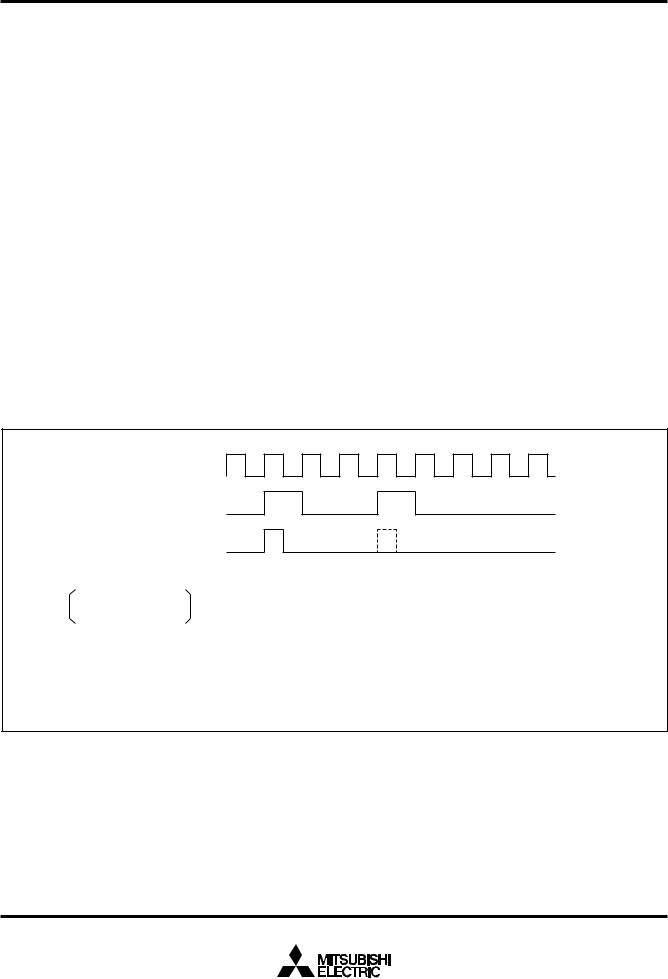
|
|
|
|
|
|
Y |
|
PRELIMINAR |
|
||||||
|
|
|
|
|
|
. . |
|
|
|
|
|
|
specification |
change |
|
|
|
|
|
|
|
to |
|
|
|
|
a |
final |
|
subject |
|
|
is |
not |
are |
|
|
||
|
limits |
|
|
|
|||
This |
|
|
|
|
|||
|
|
|
|
|
|||
|
|
|
|
|
|
|
|
Notice:parametric |
|
|
|
|
|
||
Some |
|
|
|
|
|
|
|
MITSUBISHI MICROCOMPUTERS
M37905M4C-XXXFP, M37905M4C-XXXSP M37905M6C-XXXFP, M37905M6C-XXXSP M37905M8C-XXXFP, M37905M8C-XXXSP
16-BIT CMOS MICROCOMPUTER
processor status register (PS) is replaced by the priority level of the accepted interrupt.
Therefore, multi-level priority interrupts are possible by resetting the interrupt disable flag I to “0” and enable further interrupts.
For reset, watchdog timer, zero divide, and address match detection interrupts, which do not have an interrupt control register, the processor interrupt level (IPL) is set as shown in Table 5.
The interrupt request bit and the interrupt priority level of each interrupt source are sampled and latched at each operation code fetch cycle while fsys is “H”. However, no sampling pulse is generated until the cycles whose number is selected by software has passed, even if the next operation code fetch cycle is generated. The detection of an interrupt which has the highest priority is performed during that time.
As shown in Figure 16, there are three different interrupt priority detection time from which one is selected by software. After the selected time has elapsed, the highest priority is determined and is processed after the currently executing instruction has been completed.
The time is selected with bits 4 and 5 of the processor mode register
0 (address 5E16) shown in Figure 11. Table 6 shows the relationship between these bits and the number of cycles. After a reset, the processor mode register 0 is initialized to “0016.” Therefore, the longest time is automatically set, however, the shortest time must be selected by software.
Table 5. Value loaded in processor interrupt level (IPL) during an interrupt
Interrupt types |
Setting value |
|
|
Reset |
0 |
|
|
Watchdog timer |
7 |
|
|
Zero divide |
Not change value of IPL. |
|
|
Address matching detection |
Not change value of IPL. |
|
|
Table 6. Relationship between interrupt priority detection time select
bit and number of cycles
Priority detection time select bit |
Number of cycles (Note) |
||
|
|
||
Bit 5 |
Bit 4 |
||
|
|||
|
|
|
|
0 |
0 |
7 cycles of fsys |
|
|
|
|
|
0 |
1 |
4 cycles of fsys |
|
|
|
|
|
1 |
0 |
2 cycles of fsys |
|
Note: For system clock fsys, refer to the section on the clock generating circuit.
fsys
Operation code fetch cycle
Sampling pulse
Priority detection time
Select one between 00 to 10 with bits 4 and 5 of processor mode register 0
(Note)
|
b5 b4 |
|
|
|
|
|
|
|
|
0 0 |
|
|
|
|
|
|
|
|
|
|
|
|
|
|
|
|
|
|
|
|
|
|
|
|
|
|
|
|
|
|
|
|
|
|
|
|
|
|
|
|
|
|
|
|
0 1 |
|
|
|
|
|
|
|
|
|
|
|
|
|
|
|
|
|
|
|
|
|
|
|
|
|
|
|
|
|
|
|
|
|
|
|
|
|
|
|
|
|
|
|
|
|
|
|
|
|
|
|
|
|
|
|
|
|
|
|
|
|
|
1 0 |
|
|
|
|
|
|
|
|
|
|
|
|
|
|
|
|
Note: This pulse resides when 2 cycles of fsys is selected.
Fig. 16 Interrupt priority detection time
24

|
|
|
|
|
|
Y |
|
PRELIMINAR |
|
||||||
|
|
|
|
|
|
. . |
|
|
|
|
|
|
specification |
change |
|
|
|
|
|
|
|
to |
|
|
|
|
a |
final |
|
subject |
|
|
is |
not |
are |
|
|
||
|
|
|
|
||||
|
limits |
|
|
|
|||
This |
|
|
|
|
|||
|
|
|
|
|
|||
|
|
|
|
|
|
|
|
Notice:parametric |
|
|
|
|
|
||
Some |
|
|
|
|
|
|
|
MITSUBISHI MICROCOMPUTERS
M37905M4C-XXXFP, M37905M4C-XXXSP M37905M6C-XXXFP, M37905M6C-XXXSP M37905M8C-XXXFP, M37905M8C-XXXSP
16-BIT CMOS MICROCOMPUTER
7 |
6 |
5 |
4 |
3 |
2 |
1 |
0 |
|
Address |
|
|
|
|
|
|
|
|
Port P2 pin function control register |
AE16 |
|
|
|
|
|
|
|
|
|
|
Pin TB0IN select bit
0: Allocate pin TB0IN to P55. 1: Allocate pin TB0IN to P24.
Pin TB1IN select bit
0: Allocate pin TB1IN to P56. 1: Allocate pin TB1IN to P25.
Pin TB2IN select bit
0: Allocate pin TB2IN to P57. 1: Allocate pin TB2IN to P26.
Fig. 17 Bit configuration of port P2 pin function control register
25
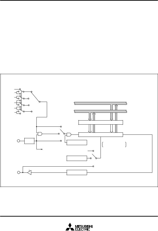
|
|
|
|
|
|
Y |
|
PRELIMINAR |
|
||||||
|
|
|
|
|
|
. . |
|
|
|
|
|
|
specification |
change |
|
|
|
|
|
|
|
to |
|
|
|
|
a |
final |
|
subject |
|
|
is |
not |
are |
|
|
||
|
limits |
|
|
|
|||
This |
|
|
|
|
|||
|
|
|
|
|
|||
|
|
|
|
|
|
|
|
Notice:parametric |
|
|
|
|
|
||
Some |
|
|
|
|
|
|
|
MITSUBISHI MICROCOMPUTERS
M37905M4C-XXXFP, M37905M4C-XXXSP M37905M6C-XXXFP, M37905M6C-XXXSP M37905M8C-XXXFP, M37905M8C-XXXSP
16-BIT CMOS MICROCOMPUTER
TIMER
There are eight 16-bit timers. They are divided by type into timer A (10) and timer B (3).
The timer I/O pins are multiplexed with I/O pins for ports P2, P4, P5 and P6. To use these pins as timer input pins, the port direction register bit corresponding to the pin must be cleared to “0” to specify input mode.
TIMER A
Figure 18 shows a block diagram of timer A.
Timer A has four modes: timer mode, event counter mode, one-shot pulse mode, and pulse width modulation mode. The mode is selected with bits 0 and 1 of the timer Ai mode register (i = 0 to 9). Each of these modes is described below.
Figure 19 shows the bit configuration of the timer A clock division select register. Timers A0 to A9 use the count source which has been selected by bits 0 and 1 of this register.
(1) Timer mode [00]
Figure 20 shows the bit configuration of the timer Ai mode register in the timer mode. Bits 0, 1 and 5 of the timer Ai mode register must be
“0” in timer mode. The timer A’s count source is selected by bits 6 and 7 of the timer Ai mode register and the contents of the timer A clock division select register. (See Table 7.)
The counting of the selected clock starts when the count start bit is
“1” and stops when it is “0”.
Figure 21 shows the bit configuration of the count start bit. The counter is decremented, an interrupt is caused and the interrupt request bit in the timer Ai interrupt control register is set when the contents becomes 000016. At the same time, the contents of the reload register is transferred to the counter and count is continued.
Timer A clock |
|
|
division select bit |
Count source |
|
f2 |
||
select bits |
||
f1 |
|
|
f16 |
|
|
f64 |
Data bus (odd) |
f512
Data bus (even)
f4096
(Low-order 8 bits) |
(High-order 8 bits) |
• Timer
• One-shot pulse Reload register(16)
• Pulse width
Timer (gate function)
Counter (16)
Polarity |
Event counter |
|
|
selection |
Count start registers 0, 1 |
TAiIN |
|
(i = 0–9) |
(Addresses 4016, 4116) |
|
External trigger |
|
Countdown |
|
Up-down registers 0, 1 |
|
(Addresses 4416, C416) |
Pulse output |
|
|
Toggle flip-flop |
TAiOUT |
|
(i = 0–9) |
|
Countup/Countdown switching “Countdown” is always selected when not in the event counter mode.
|
Addresses |
|
Addresses |
||
Timer A0 4716 |
4616 |
Timer A5 C716 |
C616 |
||
Timer A1 |
4916 |
4816 |
Timer A6 |
C916 |
C816 |
Timer A2 |
4B16 |
4A16 |
Timer A7 |
CB16 |
CA16 |
Timer A3 |
4D16 |
4C16 |
Timer A8 |
CD16 |
CC16 |
Timer A4 |
4F16 |
4E16 |
Timer A9 |
CF16 |
CE16 |
Fig. 18 Block diagram of timer A
26

|
|
|
|
|
|
Y |
|
PRELIMINAR |
|
||||||
|
|
|
|
|
|
. . |
|
|
|
|
|
|
specification |
change |
|
|
|
|
|
|
|
to |
|
|
|
|
a |
final |
|
subject |
|
|
is |
not |
are |
|
|
||
|
|
|
|
||||
|
limits |
|
|
|
|||
This |
|
|
|
|
|||
|
|
|
|
|
|||
|
|
|
|
|
|
|
|
Notice:parametric |
|
|
|
|
|
||
Some |
|
|
|
|
|
|
|
MITSUBISHI MICROCOMPUTERS
M37905M4C-XXXFP, M37905M4C-XXXSP M37905M6C-XXXFP, M37905M6C-XXXSP M37905M8C-XXXFP, M37905M8C-XXXSP
16-BIT CMOS MICROCOMPUTER
When bit 2 of the timer Ai mode register is “1”, the output is generated from TAiOUT pin. The output is toggled each time the contents of the counter reaches to 000016. When the contents of the count start bit is “0”, “L” is output from TAiOUT pin.
When bit 2 is “0”, TAiOUT can be used as a normal port pin. When bit 4 is “0”, TAiIN can be used as a normal port pin.
When bit 4 is “1”, counting is performed only while the input signal from the TAiIN pin is “H” or “L” as shown in Figure 22. Therefore, this can be used to measure the pulse width of the TAiIN input signal. Whether to count while the input signal is “H” or while it is “L” is determined by bit 3. If bit 3 is “1”, counting is performed while the TAiIN pin input signal is “H” and if bit 3 is “0”, counting is performed while it is “L”.
Note that, the duration of “H” or “L” on the TAiIN pin must be 2 or more cycles of the timer count source.
When data is written to timer Ai register with timer Ai halted, the same data is also written to the reload register and the counter. When data is written to timer Ai which is busy, the data is written to the reload register, but not to the counter. The new data is reloaded from the reload register to the counter at the next reload time and counting continues. The contents of the counter can be read at any time.
When the value set in the timer Ai register is n, the timer frequency division ratio is 1/(n+1).
7 |
6 |
5 |
4 |
3 |
2 |
1 |
0 |
Address |
|
|
|
|
|
|
|
Timer A clock division select register |
4516 |
|
|
|
|
|
|
|
Timer A clock division select bit |
|
|
|
|
|
|
|
|
(See Table 7.) |
|
Fig. 19 Bit configuration of timer A clock division select register
Table 7. Relationship between timer A clock division select bits, clock source select bits, and count source
Clock source select bits |
Timer A clock division select bits |
||||
(bits 7 and 6 at addresses |
|||||
5616 to 5A16) |
(bits 1 and 0 at address 4516) |
||||
(bits 7 and 6 at addresses |
|
|
|
|
|
D616 to DA16) |
00 |
01 |
10 |
11 |
|
0 0 |
f2 |
f1 |
f1 |
|
|
0 1 |
f16 |
f16 |
f64 |
|
Do not |
1 0 |
f64 |
f64 |
f512 |
|
select. |
1 1 |
f512 |
f4096 |
f4096 |
|
|
Note: Timers A0 to A9 use the same clock, which is selected by the timer A clock division select bits.
7 |
6 |
5 |
4 |
3 |
2 |
1 |
0 |
|
|
0 |
|
|
|
0 |
0 |
|
|
|
|
|
|
|
|
|
Addresses |
Timer A0 mode register |
5616 |
Timer A1 mode register |
5716 |
Timer A2 mode register |
5816 |
Timer A3 mode register |
5916 |
Timer A4 mode register |
5A16 |
|
Addresses |
Timer A5 mode register |
D616 |
Timer A6 mode register |
D716 |
Timer A7 mode register |
D816 |
Timer A8 mode register |
D916 |
Timer A9 mode register |
DA16 |
0 0 : Always “00” in timer mode
0 : No pulse output (TAiOUT is normal port pin.) 1 : Pulse output (TAiOUT is pulse output pin.)
0 × : No gate function (TAiIN is normal port pin.) 1 0 : Count only while TAiIN input is “L”.
1 1 : Count only while TAiIN input is “H”.
0 : Always “0” in timer mode.
Clock source select bits
See Table 7.
Fig. 20 Bit configuration of timer Ai mode register in timer mode
27
|
|
|
|
|
|
Y |
|
PRELIMINAR |
|
||||||
|
|
|
|
|
|
. . |
|
|
|
|
|
|
specification |
change |
|
|
|
|
|
|
|
to |
|
|
|
|
a |
final |
|
subject |
|
|
is |
not |
are |
|
|
||
|
limits |
|
|
|
|||
This |
|
|
|
|
|||
|
|
|
|
|
|||
|
|
|
|
|
|
|
|
Notice:parametric |
|
|
|
|
|
||
Some |
|
|
|
|
|
|
|
MITSUBISHI MICROCOMPUTERS
M37905M4C-XXXFP, M37905M4C-XXXSP M37905M6C-XXXFP, M37905M6C-XXXSP M37905M8C-XXXFP, M37905M8C-XXXSP
16-BIT CMOS MICROCOMPUTER
7 |
6 |
5 |
4 |
3 |
2 |
1 |
0 |
Count start register 0 |
Address |
7 |
6 |
5 |
4 |
3 |
2 |
1 |
0 |
Count start register 1 |
Address |
|
|
|
|
|
|
|
|
|
|
|
|
|
|
|
|
||||
|
|
|
|
|
|
|
|
(Stopped at “0”, Started at “1”) |
4016 |
|
|
|
|
|
|
|
|
(Stopped at “0”, Started at “1”) |
4116 |
|
|
|
|
|
|
|
|
Timer A0 count start bit |
|
|
|
|
|
|
|
|
|
Timer A5 count start bit |
|
|
|
|
|
|
|
|
|
Timer A1 count start bit |
|
|
|
|
|
|
|
|
|
Timer A6 count start bit |
|
|
|
|
|
|
|
|
|
Timer A2 count start bit |
|
|
|
|
|
|
|
|
|
Timer A7 count start bit |
|
|
|
|
|
|
|
|
|
Timer A3 count start bit |
|
|
|
|
|
|
|
|
|
Timer A8 count start bit |
|
|
|
|
|
|
|
|
|
Timer A4 count start bit |
|
|
|
|
|
|
|
|
|
Timer A9 count start bit |
|
|
|
|
|
|
|
|
|
Timer B0 count start bit |
|
|
|
|
|
|
|
|
|
|
|
|
|
|
|
|
|
|
|
Timer B1 count start bit |
|
|
|
|
|
|
|
|
|
|
|
|
|
|
|
|
|
|
|
Timer B2 count start bit |
|
|
|
|
|
|
|
|
|
|
|
Fig. 21 Bit configuration of count start register
Selected clock source fi
TAiIN
Timer mode register
Bit 4 |
Bit 3 |
1 |
0 |
|
|
Timer mode register
Bit 4 |
Bit 3 |
1 |
1 |
|
|
Fig. 22 Count waveform when gate function is available
28
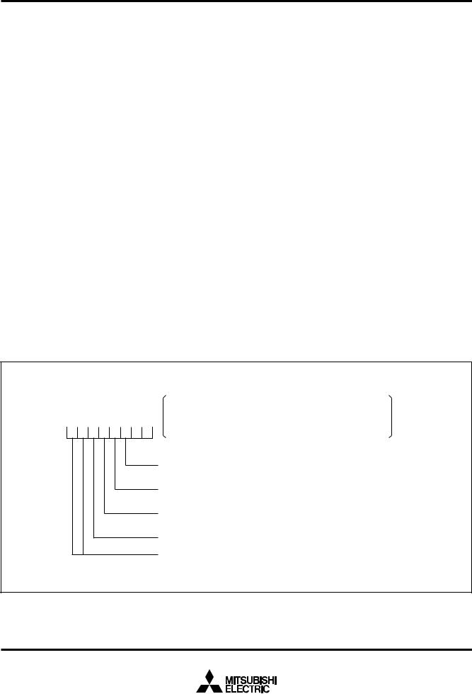
|
|
|
|
|
|
Y |
|
PRELIMINAR |
|
||||||
|
|
|
|
|
|
. . |
|
|
|
|
|
|
specification |
change |
|
|
|
|
|
|
|
to |
|
|
|
|
a |
final |
|
subject |
|
|
is |
not |
are |
|
|
||
|
|
|
|
||||
|
limits |
|
|
|
|||
This |
|
|
|
|
|||
|
|
|
|
|
|||
|
|
|
|
|
|
|
|
Notice:parametric |
|
|
|
|
|
||
Some |
|
|
|
|
|
|
|
MITSUBISHI MICROCOMPUTERS
M37905M4C-XXXFP, M37905M4C-XXXSP M37905M6C-XXXFP, M37905M6C-XXXSP M37905M8C-XXXFP, M37905M8C-XXXSP
16-BIT CMOS MICROCOMPUTER
(2) Event counter mode [01]
Figure 23 shows the bit configuration of the timer Ai mode register in the event counter mode. In event counter mode, bit 0 of the timer Ai mode register must be “1” and bits 1 and 5 must be “0”.
The input signal from the TAiIN pin is counted when the count start bit shown in Figure 21 is “1” and counting is stopped when it is “0”.
Count is performed at the fall of the input signal when bit 3 is “0” and at the rise of the signal when it is “1”.
In event counter mode, whether to increment or decrement the count can be selected with the up-down bit or the input signal from the
TAiOUT pin.
When bit 4 of the timer Ai mode register is “0”, the up-down bit is used to determine whether to increment or decrement the count
(decrement when the bit is “0” and increment when it is “1”). Figure 24 shows the bit configuration of the up-down register.
When bit 4 of the timer Ai mode register is “1”, the input signal from the TAiOUT pin is used to determine whether to increment or decrement the count. However, note that bit 2 must be “0” if bit 4 is “1”. It is because if bit 2 is “1”, TAiOUT pin becomes an output pin to output pulses.
The count is decremented when the input signal from the TAiOUT pin is “L” and incremented when it is “H”. Determine the level of the input signal from the TAiOUT pin before a valid edge is input to the TAiIN pin.
An interrupt request signal is generated and the interrupt request bit in the timer Ai interrupt control register is set when the counter reaches 000016 (decrement count) or FFFF16 (increment count). At the same time, the contents of the reload register is transferred to the counter and the count is continued.
When bit 2 is “1”, each time the counter reaches 000016 (decrement
count) or FFFF16 (increment count), the waveform’s polarity is reversed and is output from TAiOUT pin.
If bit 2 is “0”, TAiOUT pin can be used as a normal port pin.
However, if bit 4 is “1” and the TAiOUT pin is used as an output pin, the output from the pin changes the count direction. Therefore, bit 4 must be “0” unless the output from the TAiOUT pin is to be used to select the count direction.
Data write and data read are performed in the same way as for timer mode. That is, when data is written to timer Ai halted, it is also written to the reload register and the counter. When data is written to timer Ai which is busy, the data is written to the reload register, but not to the counter. The counter is reloaded with new data from the reload register at the next reload time. The counter can be read at any time.
In event counter mode, whether to increment or decrement the counter can also be determined by supplying two kinds of pulses of which phases differ by 90° to timer A2, A3, A4, A7, A8 or A9. There are two types of two-phase pulse processing operations. One uses timers A2, A3, A7, and A8 and the other uses timers A4 and A9. In both processing operations, two pulses described above are input to the TAjOUT (j = 2 to 4, 7 to 9) pin and TAjIN pin respectively.
When timers A2, A3, A7, and A8 are used, as shown in Figure 25, the count is incremented when a rising edge is input to the TAkIN (k=2,
3, 7, 8) pin after the level of TAkOUT pin changes from “L” to “H”, and when the falling edge is input, the count is decremented.
For timers A4 and A9, as shown in Figure 26, when a phase-related pulse with a rising edge input to the TAlIN (l = 4, 9) pin is input after the level of TAlOUT pin changes from “L” to “H”, the count is incremented at the respective rising edge and falling edge of the
TAlOUT pin and TAlIN pin.
|
|
|
|
|
|
|
Addresses |
|
Addresses |
|
|
|
|
|
|
Timer A0 mode register |
5616 |
Timer A5 mode register |
D616 |
|
|
|
|
|
|
Timer A1 mode register |
5716 |
Timer A6 mode register |
D716 |
7 |
6 |
5 |
4 3 |
2 1 |
0 |
Timer A2 mode register |
5816 |
Timer A7 mode register |
D816 |
Timer A3 mode register |
5916 |
Timer A8 mode register |
D916 |
||||||
× |
× |
0 |
|
0 |
1 |
Timer A4 mode register |
5A16 |
Timer A9 mode register |
DA16 |

 0 1 : Always “01” in event counter mode
0 : No pulse output
1 : Pulse output
0 : Count at the falling edge of input signal 1 : Count at the rising edge of input signal
0 : Increment or decrement according to up/down bit
1 : Increment or decrement according to TAiOUT pin input signal level
0 : Always “0” in event counter mode
× × : Not used in event counter mode
Fig. 23 Bit configuration of timer Ai mode register in event counter mode
29

|
|
|
|
|
|
Y |
|
PRELIMINAR |
|
||||||
|
|
|
|
|
|
. . |
|
|
|
|
|
|
specification |
change |
|
|
|
|
|
|
|
to |
|
|
|
|
a |
final |
|
subject |
|
|
is |
not |
are |
|
|
||
|
limits |
|
|
|
|||
This |
|
|
|
|
|||
|
|
|
|
|
|||
|
|
|
|
|
|
|
|
Notice:parametric |
|
|
|
|
|
||
Some |
|
|
|
|
|
|
|
MITSUBISHI MICROCOMPUTERS
M37905M4C-XXXFP, M37905M4C-XXXSP M37905M6C-XXXFP, M37905M6C-XXXSP M37905M8C-XXXFP, M37905M8C-XXXSP
16-BIT CMOS MICROCOMPUTER
7 6 5 4 3 2 1 0 |
|
|
Address |
7 6 5 4 3 2 1 0 |
|
|
Address |
||||||||||||||||||||||||||||||
|
|
|
|
|
|
|
|
|
|
|
|
|
|
|
|
|
Up-down register 0 |
4416 |
|
|
|
|
|
|
|
|
|
|
|
|
|
|
|
|
|
Up-down register 1 |
C416 |
|
|
|
|
|
|
|
|
|
|
|
|
|
|
|
|
|
Timer A0 up-down bit |
|
|
|
|
|
|
|
|
|
|
|
|
|
|
|
|
|
|
Timer A5 up-down bit |
|
|
|
|
|
|
|
|
|
|
|
|
|
|
|
|
|
|
|
|
|
|
|
|
|
|
|
|
|
|
|
|
|
|
|
|
|
||
|
|
|
|
|
|
|
|
|
|
|
|
|
|
|
|
|
Timer A1 up-down bit |
|
|
|
|
|
|
|
|
|
|
|
|
|
|
|
|
|
|
Timer A6 up-down bit |
|
|
|
|
|
|
|
|
|
|
|
|
|
|
|
|
|
|
|
|
|
|
|
|
|
|
|
|
|
|
|
|
|
|
|
|
|
||
|
|
|
|
|
|
|
|
|
|
|
|
|
|
|
|
|
Timer A2 up-down bit |
|
|
|
|
|
|
|
|
|
|
|
|
|
|
|
|
|
|
Timer A7 up-down bit |
|
|
|
|
|
|
|
|
|
|
|
|
|
|
|
|
|
|
|
|
|
|
|
|
|
|
|
|
|
|
|
|
|
|
|
|
|
||
|
|
|
|
|
|
|
|
|
|
|
|
|
|
|
|
|
Timer A3 up-down bit |
|
|
|
|
|
|
|
|
|
|
|
|
|
|
|
|
|
|
Timer A8 up-down bit |
|
|
|
|
|
|
|
|
|
|
|
|
|
|
|
|
|
|
|
|
|
|
|
|
|
|
|
|
|
|
|
|
|
|
|
|
|
||
|
|
|
|
|
|
|
|
|
|
|
|
|
|
|
|
|
Timer A4 up-down bit |
|
|
|
|
|
|
|
|
|
|
|
|
|
|
|
|
|
|
Timer A9 up-down bit |
|
|
|
|
|
|
|
|
|
|
|
|
|
|
|
|
|
|
|
|
|
|
|
|
|
|
|
|
|
|
|
|
|
|
|
|
|
||
|
|
|
|
|
|
|
|
|
|
|
|
|
|
|
|
|
Timer A2 two-phase pulse signal |
|
|
|
|
|
|
|
|
|
|
|
|
|
|
|
|
|
Timer A7 two-phase pulse signal |
||
|
|
|
|
|
|
|
|
|
|
|
|
|
|
|
|
|
|
|
|
|
|
|
|
|
|
|
|
|
|
|
|
|
|
||||
|
|
|
|
|
|
|
|
|
|
|
|
|
|
|
|
|
processing select bit |
|
|
|
|
|
|
|
|
|
|
|
|
|
|
|
|
|
|
processing select bit |
|
|
|
|
|
|
|
|
|
|
|
|
|
|
|
|
|
|
0 : Two-phase pulse signal processing |
|
|
|
|
|
|
|
|
|
|
|
|
|
|
|
|
|
0 : Two-phase pulse signal processing |
||
|
|
|
|
|
|
|
|
|
|
|
|
|
|
|
|
|
disabled |
|
|
|
|
|
|
|
|
|
|
|
|
|
|
|
|
|
|
disabled |
|
|
|
|
|
|
|
|
|
|
|
|
|
|
|
|
|
|
1 : Two-phase pulse signal processing |
|
|
|
|
|
|
|
|
|
|
|
|
|
|
|
|
|
1 : Two-phase pulse signal processing |
||
|
|
|
|
|
|
|
|
|
|
|
|
|
|
|
|
|
mode |
|
|
|
|
|
|
|
|
|
|
|
|
|
|
|
|
|
|
mode |
|
|
|
|
|
|
|
|
|
|
|
|
|
|
|
|
|
|
Timer A3 two-phase pulse signal |
|
|
|
|
|
|
|
|
|
|
|
|
|
|
|
|
|
Timer A8 two-phase pulse signal |
||
|
|
|
|
|
|
|
|
|
|
|
|
|
|
|
|
|
|
|
|
|
|
|
|
|
|
|
|
|
|
|
|
|
|
||||
|
|
|
|
|
|
|
|
|
|
|
|
|
|
|
|
|
processing select bit |
|
|
|
|
|
|
|
|
|
|
|
|
|
|
|
|
|
|
processing select bit |
|
|
|
|
|
|
|
|
|
|
|
|
|
|
|
|
|
|
0 : Two-phase pulse signal processing |
|
|
|
|
|
|
|
|
|
|
|
|
|
|
|
|
|
0 : Two-phase pulse signal processing |
||
|
|
|
|
|
|
|
|
|
|
|
|
|
|
|
|
|
disabled |
|
|
|
|
|
|
|
|
|
|
|
|
|
|
|
|
|
|
disabled |
|
|
|
|
|
|
|
|
|
|
|
|
|
|
|
|
|
|
1 : Two-phase pulse signal processing |
|
|
|
|
|
|
|
|
|
|
|
|
|
|
|
|
|
1 : Two-phase pulse signal processing |
||
|
|
|
|
|
|
|
|
|
|
|
|
|
|
|
|
|
mode |
|
|
|
|
|
|
|
|
|
|
|
|
|
|
|
|
|
|
mode |
|
|
|
|
|
|
|
|
|
|
|
|
|
|
|
|
|
|
Timer A4 two-phase pulse signal |
|
|
|
|
|
|
|
|
|
|
|
|
|
|
|
|
|
Timer A9 two-phase pulse signal |
||
|
|
|
|
|
|
|
|
|
|
|
|
|
|
|
|
|
|
|
|
|
|
|
|
|
|
|
|
|
|
|
|
|
|
||||
|
|
|
|
|
|
|
|
|
|
|
|
|
|
|
|
|
processing select bit |
|
|
|
|
|
|
|
|
|
|
|
|
|
|
|
|
|
|
processing select bit |
|
|
|
|
|
|
|
|
|
|
|
|
|
|
|
|
|
|
0 : Two-phase pulse signal processing |
|
|
|
|
|
|
|
|
|
|
|
|
|
|
|
|
|
0 : Two-phase pulse signal processing |
||
|
|
|
|
|
|
|
|
|
|
|
|
|
|
|
|
|
disabled |
|
|
|
|
|
|
|
|
|
|
|
|
|
|
|
|
|
|
disabled |
|
|
|
|
|
|
|
|
|
|
|
|
|
|
|
|
|
|
1 : Two-phase pulse signal processing |
|
|
|
|
|
|
|
|
|
|
|
|
|
|
|
|
|
1 : Two-phase pulse signal processing |
||
|
|
|
|
|
|
|
|
|
|
|
|
|
|
|
|
|
mode |
|
|
|
|
|
|
|
|
|
|
|
|
|
|
|
|
|
|
mode |
|
Fig. 24 Bit configuration of up-down register
When a phase-related pulse with a falling edge input to the TAkOUT pin is input after the level of TAlIN pin changes from “H” to “L”, the count is decremented at the respective rising edge and falling edge of the TAlIN pin and TAlOUT pin. When performing this two-phase pulse signal processing, bits 0 and 4 of timer Aj mode register must be set to “1” and bits 1, 2, 3, and 5 must be “0”. Bits 6 and 7 are ignored. (See Figure 27.) Note that bits 5, 6, and 7 of the up-down register 0 (address 4416) are the two-phase pulse signal processing select bits for timers A2, A3, and A4, respectively. Also, bits 5, 6, and
7 of the up-down register 1 (address C416) are the two-phase pulse signal processing select bits for timers A7, A8, and A9, respectively.
Each timer operates in normal event counter mode when the corresponding bit is “0” and performs two-phase pulse signal processing when it is “1”.
Count is started by setting the count start bit to “1”. Data write and read are performed in the same way as for normal event counter mode. Note that the direction register of the input port must be set to input mode because two kinds of pulse signals, described above, are input. Also, there can be no pulse output in this mode.
TAkOUT |
|
|
|
|
|
|
|
|
|
|
|
|
|
|
|
|
|
|
|
|
|
|
|
|
|
|
|
|
|
|
|
|
|
|
|
|
|
|
|
|
|
|
|
|
|
TAkIN |
|
|
|
|
|
|
|
|
|
|
|
|
|
|
|
|
|
|
|
|
||
|
|
|
|
|
|
|
|
|
|
|
|
|
|
|
|
|
|
|
||||
(k = 2, 3, 7, 8) Incre- |
Incre- |
Incre- |
DecreDecreDecre- |
|||||||||||||||||||
|
|
ment- |
ment- |
ment- |
ment- |
ment- |
ment- |
|||||||||||||||
|
|
count |
count |
count |
count |
count |
count |
|||||||||||||||
Fig. 25 Two-phase pulse processing operation of timer A2, A3, A7,
A8
TAlOUT |
|
|
|
|
|
|
|
|
|
|
|
|
|
|
|
|
|
|
|
|
|
|
|
|
|
|
|
|
|
|
|
|
|
|
|
|
|
|
|
|
|
|
|
|
|
|
|
|
|
|
|
|
|||||||||||||||||||
Increment-count at each edge |
Decrement-count at each edge |
||||||||||||||||||||||
TAlIN |
|
|
|
|
|
|
|
|
|
|
|
|
|
|
|
|
|
||||||
|
|
|
|
|
|
|
|
|
|
|
|
|
|
|
|
|
|||||||
(l = 4, 9) |
|
|
|
|
|
|
|
|
|
|
|
|
|
|
|
|
|
|
|||||
|
|
|
|||||||||||||||||||||
|
|
|
|||||||||||||||||||||
Increment-count at each edge |
Decrement-count at each edge |
||||||||||||||||||||||
Fig. 26 Two-phase pulse processing operation of timers A4 and A9
7 |
6 |
5 |
4 |
3 |
2 |
1 |
0 |
|
||||||||
× |
|
× |
|
0 |
1 |
0 |
0 |
0 |
1 |
|
||||||
|
|
|
|
|
|
|
|
|
|
|
|
|
|
|
|
|
|
|
|
|
|
|
|
|
|
|
|
|
|
|
|
|
|
|
|
|
|
|
|
|
|
|
|
|
|
|
|
|
|
|
|
|
|
|
|
|
|
|
|
|
|
|
|
|
|
|
|
|
Addresses |
Timer A2 mode register |
5816 |
Timer A3 mode register |
5916 |
Timer A4 mode register |
5A16 |
Timer A7 mode register |
C816 |
Timer A8 mode register |
C916 |
Timer A9 mode register |
CA16 |
0 1 : Always “01” in event counter mode
0 1 0 0 : Always “0100” when processing two-phase pulse signal
× × : Not used in event counter mode
Fig. 27 Bit configuration of timer Aj mode register when performing two-phase pulse signal processing in event counter mode
30
Loading...