


M37754S4CHP
Table of contents
 Loading...
Mitsubishi M37754S4CHP, M37754S4CGP, M37754M8C-XXXGP, M37902FJCHP, M37902FGCHP Datasheet
...
Y
MITSUBISHI MICROCOMPUTERS
M37754M8C-XXXGP, M37754M8C-XXXHP
PRELIMINAR
Notice: This is not a final specification.
Some parametric limits are subject to change.
M37754S4CGP, M37754S4CHP
DESCRIPTION
The M37754M8C-XXXGP is a single-chip microcomputer designed
with high-performance CMOS silicon gate technology . This is housed
in a 100-pin plastic molded QFP.
This microcomputer has a CPU and a bus interface unit. The CPU is
a 16-bit parallel processor that can also be switched to perform 8-bit
parallel processing, and the bus interface unit enhances the memory
access efficiency to execute instructions fast.
In addition to the 7700 Family basic instructions, the M37754M8CXXXGP has 6 special instructions which contain instructions for
signed multiplication/division; these added instructions improve the
servo arithmetic performance to control hard disk drives and so on.
This microcomputer also include the ROM, RAM, multiple-function
timers, motor control function, serial I/O, A-D converter, D-A converter, and so on.
The differences between M37754M8C-XXXGP, M37754M8C-XXXHP,
M37754S4CGP and M37754S4CHP are listed in the table on the
next page: the internal ROM, usable processor mode, and package.
Therefore, the following descriptions will be for the M37754M8CXXXGP unless otherwise noted.
DISTINCTIVE FEATURES
Number of basic machine instructions .................................... 109
•
(103 basic instructions of 7700 Family + 6 special instructions)
Memory size ROM ................................................ 60 Kbytes
•
RAM................................................2048 bytes
SINGLE-CHIP 16-BIT CMOS MICROCOMPUTER
Instruction execution time
•
The fastest instruction at 40 MHz frequency ...................... 100 ns
Single power supply ...................................................... 5V ±10 %
•
Low power dissipation (at 40 MHz frequency) .......125 mW (Typ.)
•
Interrupts ........................................................... 21 types, 7 levels
•
Multiple-function 16-bit timer ...................................................5+3
•
(three-phase motor drive waveform or pulse motor control waveform output)
Serial I/O (UART or clock synchronous) ..................................... 2
•
10-bit A-D converter ............................................ 8-channel inputs
•
8-bit D-A converter ............................................ 2-channel outputs
•
12-bit watchdog timer
•
Programmable input/output
•
(ports P0—P11) ......................................................................... 87
Small package [M37754M8C-XXXHP]
•
.................................100-pin fine pitch QFP (read pitch : 0.5 mm)
APPLICATION
Control devices for personal computer peripheral equipment such as
CD-ROM drives, hard disk drives, high density FDD, printers
Control devices for office equipment such as copiers and facsimiles
Control devices for industrial equipment such as communication and
measuring instruments
Control devices for equipment required for motor control such as inverter air conditioner and general purpose inverter
M37754M8C-XXXGP PIN CONFIGURATION (TOP VIEW)
0/A0
1/A1
2/A2
3/A3
4/A4
5/A5
6/A6
7/A7
0/A8
1/A9
2/A10
3/A11
4/A12
5/A13
6/A14
7/A15
0/A16
P0
P0
P0
P0
P0
P0
P0
P0
P1
P1
P1
P1
P1
P1
P1
P1
P2
↔
↔
↔
↔
or
↔
↔
↔
↔
1/TA4IN
0/TA4OUT
P6
7/TA3IN/KI3
P6
6/TA3OUT/KI2
P5
P5
P87/TXD1
6/RXD1
P8
5/CLK1
P84/CTS1/RTS1/DA1/INT4
0/CTS0/RTS0/CLKS1/DA0
P8
P8
P8
2/RXD0/CLKS0
P8
P8
7/AN7/ADTRG
P7
P7
P7
P7
P7
P7
P7
3/TXD0
1/CLK0
CC
V
CC
AV
REF
V
SS
AV
SS
V
6/AN6
5/AN5
4/AN4
3/AN3
2/AN2
1/AN1
↔
↔
↔
↔
↔
↔
↔
↔
↔
↔
↔
↔
8079787776757473727170696867666564636261605958575655545352
↔
81 50
↔
82 49
↔
83 48
↔
84 47
↔
85 46
↔
86 45
↔
87 44
↔
88 43
89 42
90 41
→
91 40
92 39
93 38
↔
94 37
↔
95 36
↔
96 35
↔
97
↔
98 33
↔
99 32
↔
100
123456789
↔
↔
↔
P70/AN0
5/INT3/KI4
P9
↔
↔
↔
4/CS4/RTP13
P9
3/CS3/A22/RTP12
P9
2/CS2/A21/U/RTP11
P9
↔
↔
↔
0/CS0
7/TB2IN
6/TB1IN
P9
P6
P6
P91/CS1/A20/V/RTP10
↔
M37754M8C-XXXGP
M37754S4CGP
101112131415161718192021222324252627282930
↔
↔
↔
↔
4/INT2
3/INT1
2/INT0
5/TB0IN
P6
P6
P6
P6
Outline 100P6S-A
0/D0/LA0
1/D1/LA1
2/D2/LA2
3/D3/LA3
4/D4/LA4
5/D5/LA5
6/D6/LA6
7/D7/LA7
1/A17
2/A18
3/A19
7/A23
P10
P10
P10
P10
P2
P2
P2
P2
↔
↔
↔
↔
↔
↔
↔
↔
5/TA2IN/KI1
P5
↔
↔
4/TA2OUT/KI0
P5
1/TA0IN/V/RTP01
3/TA1IN/W/RTP03
2/TA1OUT/U/RTP02
P5
P5
P5
P10
↔
↔
↔
↔
↔
↔
↔
↔
7
6
5
P4
P4
P4
0/TA0OUT/W/RTP00
P5
P10
↔
↔
4
P4
P10
↔
↔
3
P4
P10
↔
↔
2/φ1
P4
0/D8
P11
↔
51
34
31
↔
1/RDY
P4
↔
P11
↔
P11
↔
P11
↔
P11
↔
P11
↔
P11
↔
P11
↔
P3
↔
P3
↔
P3
↔
P3
V
VSS
→
E/RD
→
X
←
X
←
RESET
CNV
←
BYTE
↔
P4
1/D9
2D10
3/D11
4/D12
5/D13
6/D14
7/D15
0/WR
1/BHE
2/ALE
3/HLDA
CC
OUT
IN
SS
0/HOLD

MITSUBISHI MICROCOMPUTERS
M37754M8C-XXXGP, M37754M8C-XXXHP
PRELIMINARY
Notice: This is not a final specification.
Some parametric limits are subject to change.
M37754S4CGP, M37754S4CHP
M37754M8C-XXXHP PIN CONFIGURATION (TOP VIEW)
↔ P21/A17
↔ P20/A16
↔ P17/A15
↔ P16/A14
↔ P15/A13
↔ P14/A12
↔ P13/A11
↔ P12/A10
↔ P11/A9
↔ P10/A8
↔ P07/A7
↔ P06/A6
↔ P05/A5
↔ P04/A4
P02/A2 ↔
P0
P0
7/TXD1 ↔
P8
6/RXD1 ↔
P8
5/CLK1 ↔
4/CTS1/RTS1/DA1/INT4 ↔
P8
0/CTS0/RTS0/CLKS1/DA0 ↔
P8
P8
3/TXD0 ↔
P8
2/RXD0/CLKS0 ↔
P8
1/CLK0 ↔
P8
AV
AV
7/AN7/ADTRG ↔
P7
P76/AN6 ↔
5/AN5 ↔
P7
4/AN4 ↔
P7
3/AN3 ↔
P7
2/AN2 ↔
P7
1/AN1 ↔
P7
0/AN0 ↔
P7
5/INT3/KI4 ↔
P9
1/A1 ↔
0/A0 ↔
CC
V
CC
REF →
V
SS
SS
V
↔ P03/A3
73
74
75
76
77
78
79
80
81
82
83
84
85
86
87
88
89
90
91
92
93
94
95
96
97
98
99
100
1P9
4/CS4/RTP13 ↔
2
3/CS3/A22/RTP12 ↔
P9
3
P92/CS2/A21/U/RTP11 ↔
69
70
71
72
M37754M8C-XXXHP
7
6
5
4
0/CS0 ↔
7/TB2IN ↔P66/TB1IN ↔P65/TB0IN ↔
P9
P6
P91/CS1/A20/V/RTP10 ↔
65
66
67
68
M37754S4CHP
9
8
11
10
4/INT2 ↔
P63/INT1 ↔
P62/INT0 ↔
P6
64
12
1/TA4IN ↔
P6
or
63
13
0/TA4OUT ↔
P6
62
14
7/TA3IN/KI3 ↔
P5
61
15
6/TA3OUT/KI2 ↔
P5
SINGLE-CHIP 16-BIT CMOS MICROCOMPUTER
↔ P106/D6/LA6
↔ P105/D5/LA5
↔ P104/D4/LA4
↔ P103/D3/LA3
↔ P102/D2/LA2
↔ P101/D1/LA1
↔ P100/D0/LA0
↔ P27/A23
↔ P23/A19
↔ P22/A18
60
16
5/TA2IN/KI1 ↔
P5
59
17
4/TA2OUT/KI0 ↔
P5
58
18
3/TA1IN/W/RTP03 ↔
P5
57
19
2/TA1OUT/U/RTP02 ↔
P5
56
20
1/TA0IN/V/RTP01 ↔
P5
55
21
0/TA0OUT/W/RTP00 ↔
P5
52
53
54
24
23
22
7 ↔P46 ↔P45 ↔P44 ↔
P4
51
50
↔ P107/D7/LA7
49
↔ P110/D8
48
↔ P111/D9
47
↔ P112/D10
46
↔ P113/D11
45
↔ P114/D12
44
↔ P115/D13
43
↔ P116/D14
42
↔ P11
41
↔ P3
40
↔ P3
39
↔ P3
38
↔ P33/HLDA
37
VCC
36
V
SS
35
→ E/RD
34
→ XOUT
33
← X
IN
32
← RESET
31
CNV
30
← BYTE
↔ P4
29
↔ P41/RDY
28
↔ P42/φ1
2627↔ P43
25
7/D15
0/WR
1/BHE
2/ALE
SS
0/HOLD
Outline 100P6Q-A
Differences between M37754M8C-XXXGP, M37754M8C-XXXHP, M37754S4CGP, and M37754S4CHP
Product
M37754M8C-XXXGP
M37754M8C-XXXHP
M37754S4CGP
M37754S4CHP
Internal ROM
Equipped
(60 Kbytes)
Not equipped
(External ROM)
Usable processor mode
•
Single-chip mode
•
Memory expansion mode
•
Microprocessor mode
•
Microprocessor mode
Package
100-pin QFP (100P6S-A)
100-pin fine pitch QFP
(100P6Q-A)
100-pin QFP (100P6S-A)
100-pin fine pitch QFP (100P6Q-A)
2
MITSUBISHI MICROCOMPUTERS
M37754M8C-XXXGP, M37754M8C-XXXHP
PRELIMINARY
Notice: This is not a final specification.
Some parametric limits are subject to change.
BYTE
Bus width
select input
VREF
Reference
voltage input
CC
(5V)
AV
Instruction Register(8)
SS
(0V)
AV
SS
CNV
Data Buffer DB
Data Buffer DB
Instruction Queue Buffer Q0(8)
Instruction Queue Buffer Q
Instruction Queue Buffer Q
Incrementer(24)
Program Address Register PA(24)
Data Address Register DA(24)
H(8)
L(8)
1
(8)
2
(8)
M37754S4CGP, M37754S4CHP
SINGLE-CHIP 16-BIT CMOS MICROCOMPUTER
Data Bus(Even)
Data Bus(Odd)
Address Bus
Converter(8)
1
D-A
Converter(8)
0
D-A
(8)
P0
(8)
P1
(5)
P2
(4)
P3
(8)
P10
port P0
Input/Output
port P1
Input/Output
port P2
Input/Output
port P3
Input/Output
port P10
Input/Output
SS
V
(0V)
CC
V
(5V)
RESET
Reset input
E
Enable output
XOUT
Clock output
Clock Generating Circuit
XIN
Clock input
BLOCK DIAGRAM
Incrementer/Decrementer(24)
Program Counter PC(16)
Program Bank Register PG(8)
Data Bank Register DT(8)
Input Buffer Register IB(16)
Processor Status Register PS(11)
Direct Page Register DPR(16)
Stack Pointer S(16)
Index Register Y(16)
Index Register X(16)
Accumulator B(16)
Accumulator A(16)
Arithmetic Logic
Unit(16)
WatchdogTimer
Timer TA3(16)
Timer TA4(16)
UART 1(9)
Timer TB1(16)
Timer TB2(16)
Timer TA1(16)
Timer TA2(16)
RAM
2048 Bytes
ROM
60 Kbytes
A-D Converter(10)
UART 0(9)
Timer TB0(16)
Timer TA0(16)
P11(8)
P4(8)
P8(8) P7(8)P9(6) P6(8) P5(8)
port P11
Input/Output
port P4
Input/Output
port P5
Input/Output
port P6
Input/Output
port P7
Input/Output
port P8
Input/Output
port P9
Input/Output
3
MITSUBISHI MICROCOMPUTERS
M37754M8C-XXXGP, M37754M8C-XXXHP
PRELIMINARY
Notice: This is not a final specification.
Some parametric limits are subject to change.
FUNCTIONS OF M37754M8C-XXXGP
Number of basic machine instructions
Instruction execution time
Memory size
Input/Output ports (Note 2)
Multiple-function timers
Serial I/O
A-D converter
D-A converter
Watchdog timer
Short-circuit prevention time set timer
Interrupts
Clock generating circuit
Supply voltage
Power dissipation
Input/Output characteristic
Memory expansion
Operating temperature range
Device structure
Package
Notes 1: The M37754S4CGP and the M37754S4CHP are not equipped with ROM.
2: Input/Output ports for the M37754S4CGP and the M37754S4CHP are as shown below :
•
P5-P8, P11 (8-bit × 5)
•
P4 (5-bit × 1)
•
P9 (6-bit × 1)
ROM (Note 1)
RAM
P0, P1, P4 – P8, P10, P11
P2
P3
P9
TA0, TA1, TA2, TA3, TA4
TB0, TB1, TB2
Input/Output withstand voltage
Output current
M37754S4CGP, M37754S4CHP
SINGLE-CHIP 16-BIT CMOS MICROCOMPUTER
FunctionsParameter
109
100 ns (the fastest instruction at external clock 40 MHz frequency)
60 Kbytes
2048 bytes
8-bit × 9
5-bit × 1
4-bit × 1
6-bit × 1
16-bit × 5
16-bit × 3
(UART or clock synchronous serial I/O) × 2
10-bit × 1(8 channels)
8-bit × 2
12-bit × 1
8-bit × 3
5 external types, 16 internal types
(Each interrupt can be set to priority levels 0 – 7.)
Built-in (externally connected to a ceramic resonator or quartz crystal resonator)
5 V±10 %
125 mW(at external clock 40 MHz frequency)
5 V
5 mA
Maximum 16 Mbytes
–20 to 85 °C
CMOS high-performance silicon gate process
100-pin plastic molded QFP
4

MITSUBISHI MICROCOMPUTERS
M37754M8C-XXXGP, M37754M8C-XXXHP
PRELIMINARY
Notice: This is not a final specification.
Some parametric limits are subject to change.
M37754S4CGP, M37754S4CHP
SINGLE-CHIP 16-BIT CMOS MICROCOMPUTER
PIN DESCRIPTION (MICROCOMPUTER MODE)
Input/
Output
Input
Supply 5 V±10 % to VCC and 0 V to VSS.
This pin controls the processor mode. Connect to VSS for single-chip mode or memory
VCC, VSS
CNVSS
NamePin
Power supply
CNVSS input
expansion mode. Connect to VCC for microprocessor mode and external ROM version.
RESET
Reset input
Input
This is reset input pin. The microcomputer is reset when supplying “L” level to this
pin.
XIN
Clock input
Input
These are I/O pins of internal clock generating circuit. Connect a ceramic or quartzcrystal resonator between XIN and XOUT. When an external clock is used, the clock
XOUT
E
BYTE
(Note)
Clock output
Enable output
Bus width select input
Output
Output
Input
source should be connected to the XIN pin and the XOUT pin should be left open.
This pin outputs enable signal E, which indicates access state of data bus for
single-chip mode.
This pin outputs RD signal for memory expansion mode or microprocessor mode.
___
This pin determines whether the external data bus is 8-bit width or 16-bit width for
memory expansion mode or microprocessor mode. The width is 16 bits when “L”
signal inputs and 8 bits when “H” signal inputs.
AVCC,
AVSS
VREF
P00 – P07
Analog supply input
Reference voltage input
I/O port P0
Input
Power supply for the A-D converter and the D-A converter. Connect AVCC to VCC
and AVSS to VSS externally.
This is reference voltage input pin for the A-D converter and the D-A converter.
I/O
In single-chip mode, port P0 is an 8-bit I/O port. This port has an I/O direction
register and each pin can be programmed for input or output. These ports are in
the input mode when reset. Address (A0 - A7) is output in memory expansion mode
or microprocessor mode.
P10 – P17
I/O port P1
I/O
In single-chip mode, these pins have the same functions as port P0. Address (A8 A15) is output in memory expansion mode or microprocessor mode.
P20 – P23,
P27
P30 – P33
I/O port P2
I/O port P3
I/O
In single-chip mode, these pins have the same functions as port P0. Address (A16 A19, A23) is output in memory expansion mode or microprocessor mode.
I/O
In single-chip mode, these pins have the same functions as port P0. In memory
expansion mode or microprocessor mode, WR, BHE , ALE, and HLDA signals are
output.
P40 – P47
I/O port P4
I/O
In single-chip mode, these pins have the same functions as port P0. In memory
expansion mode or micro processor mode, P40, P41, and P42 become HOLD and
____
RDY input pins, and clock
φ
1 output pin respectively. Functions of other pins are
the same as in single-chip mode. In memory expansion mode, P42 can be
programmed as I/O port.
P50 – P57
I/O port P5
I/O
In addition to having the same functions as port P0 in single-chip mode, these pins
also function as I/O pins for timer A0, timer A1, timer A2, timer A3, output pins for
motor drive waveform, and input pins for key input interrupt.
P60 – P67
P70 – P77
I/O port P6
I/O port P7
I/O
In addition to having the same functions as port P0 in single-chip mode, these pins
also function as I/O pins for timer A4, input pins for external interrupt input INT0,
____ ____
INT1, and INT2, and input pins for timer B0, timer B1, and timer B2.
I/O
In addition to having the same functions as port P0 in single-chip mode, these pins
also function as input pins for A-D converter.
P80 – P87
P90 – P95
I/O port P8
I/O port P9
I/O
In addition to having the same functions as port P0 in single-chip mode, these pins
also function as I/O pins for UART0, UART1, output pins for D-A converter, and
input pin for INT4.
I/O
In addition to having the same functions as port P0 in single-chip mode, these pins
____
also function as input pin for INT3, output pins for motor drive waveform.
In memory expansion mode and microprocessor mode, these pins can be
programmed as address (A20 - A22) or output pins for CS0 – CS4
Note: It is impossible to change the input level of the BYTE pin in each bus cycle. In other words, bus width cannot be switched dynamically. Fix the input
level of the BYTE pin to “H” or “L” according to the bus width used.
Functions
_
___ ____ _____
_____
____
____
___ ___
5

MITSUBISHI MICROCOMPUTERS
M37754M8C-XXXGP, M37754M8C-XXXHP
PRELIMINARY
Notice: This is not a final specification.
Some parametric limits are subject to change.
NamePin
0 – P107
P10
P1 10 – P1 17
I/O port P10
I/O port P11 I/O
Input/
Output
I/O
M37754S4CGP, M37754S4CHP
SINGLE-CHIP 16-BIT CMOS MICROCOMPUTER
Functions
In single-chip mode, these pins have the same functions as port P0. In memory
expansion mode or microprocessor mode, these pins become data I/O pins and
operate as follows:
(1) When using 16-bit width as external data bus width:
Accessing external memory
•
<When reading>
Pins’ value is input into low-order internal data bus (DB0 to DB7).
<When writing>
Value of low-order internal data bus (DB0 to DB7) is output to these pins.
Accessing internal memory
•
<When reading>
These pins become high impedance.
<When writing>
Value of internal data bus is output to these pins.
(2) When using 8-bit width as external data bus width:
Accessing external memory
•
<When reading>
Pins’ value is input into internal data bus. The value is input into low-order
internal data bus (DB0 to DB7) when accessing an even address; it is input
into high-order internal data bus (DB8 to DB15) when accessing an odd
address.
<When writing>
Value of internal data bus is output to these pins. The value of low-order
internal data bus (DB0 to DB7) is output when accessing an even address;
the value of high-order internal data bus (DB8 to DB15) is output when
accessing an odd address.
Accessing internal memory
•
<When reading>
These pins become high impedance.
<When writing>
Value of internal data bus is output to these pins.
When the external bus width is 8 bits, the mode where low-order address
(LA0 – LA7) is output when RD or WR output is “H” and data (D0 – D7) is
input/output when RD or WR output is “L” can be selected in specified
external memory area access cycle.
In single-chip mode, these pins have the same functions as port P0. In memory
expansion mode or microprocessor mode, these pins operate as follows:
(1) When using 16-bit width as external data bus width
Accessing external memory
•
<When reading>
The value is input into high-order internal data bus (DB8 to DB15) when
accessing an odd address; these pins enter high impedance state when not
accessing an odd address.
<When writing>
Value of high-order internal data bus (DB8-DB15) is output to these pins.
Accessing internal memory
•
<When reading>
These pins enter high impedance state.
<When writing>
Value of internal data bus is output to these pins.
(2) When using 8-bit width as external data bus width
These pins become I/O port P110 – P117.
___ ___
___ ___
6

MITSUBISHI MICROCOMPUTERS
M37754M8C-XXXGP, M37754M8C-XXXHP
PRELIMINARY
Notice: This is not a final specification.
Some parametric limits are subject to change.
BASIC FUNCTION BLOCKS
The M37754M8C-XXXGP contains the following devices on a single
chip: ROM, RAM, CPU, bus interface unit, timers, UART, A-D converter, D-A converter, I/O ports, clock generating circuit and others.
Each of these devices is described below.
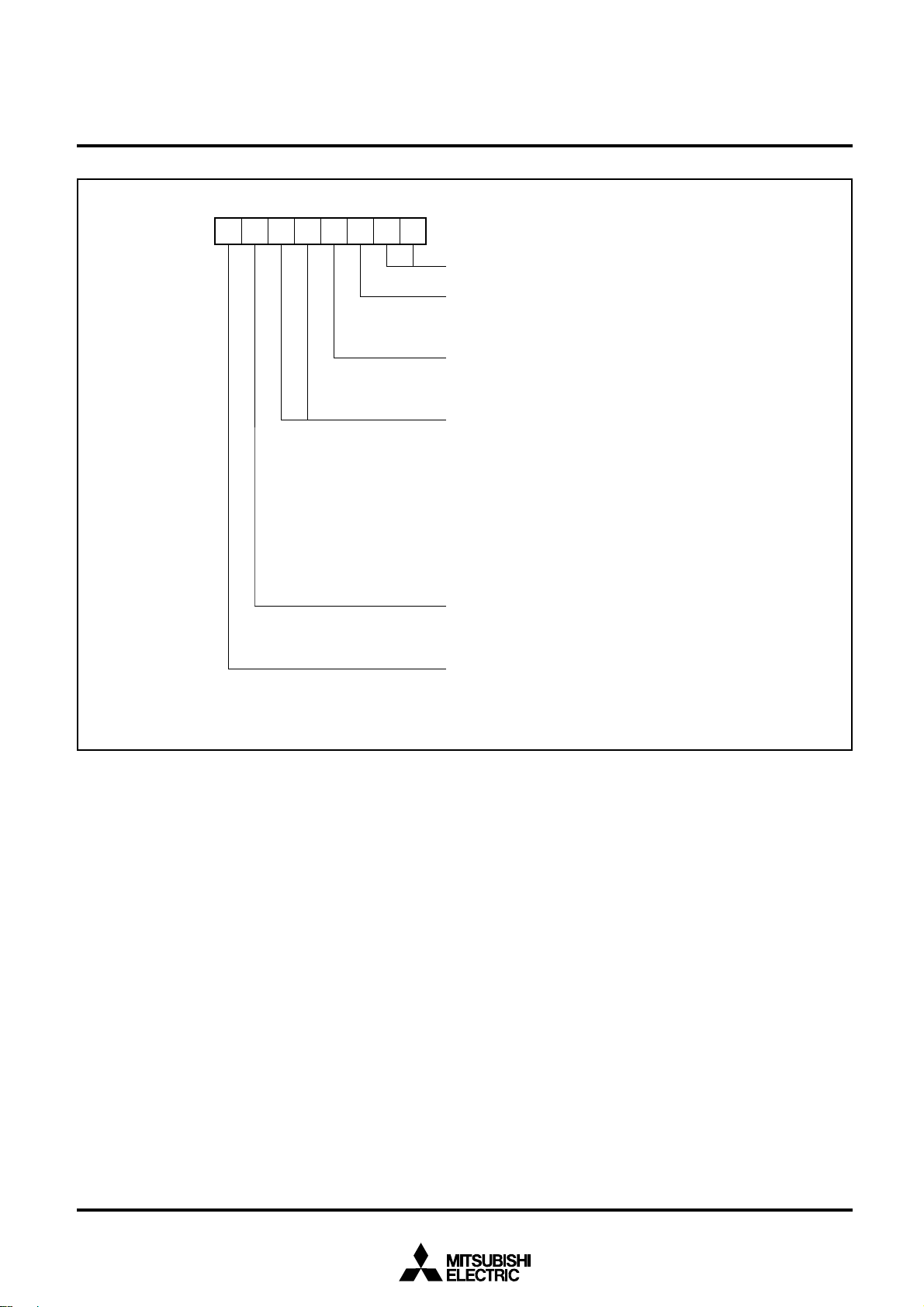
MEMORY
The memory map is shown in Figure 1. The address space is 16
Mbytes from addresses 0
vided into 64-Kbyte units called banks. The banks are numbered
from 0
16 to FF16.
Internal ROM, internal RAM, and control registers for internal peripheral devices are assigned to bank 0
The 60-Kbyte area from addresses 1000
ROM.
Bank 016
Bank 116
•
•
•
•
•
•
•
•
•
•
•
•
•
Bank FE16
Bank FF
16 to FFFFFF16. The address space is di-
16.
16 to FFFF16 is the internal
00000016
00FFFF16
01000016
01FFFF16
FE000016
FEFFFF16
FF000016
16
FFFFFF16
00000016 00000016
00007F16
00008016
00087F16
001000
00FFFF16
M37754S4CGP, M37754S4CHP
SINGLE-CHIP 16-BIT CMOS MICROCOMPUTER
Addresses FFD216 to FFFF16 are the RESET and interrupt vector
addresses and contain the interrupt vectors. Refer to the section on
interrupts for details.
The 2048-byte area from addresses 80
nal RAM. In addition to storing data, the RAM is used as stack during
a subroutine call, or interrupts.
Assigned to addresses 0
16 to 7F16 are peripheral devices such as
I/O ports, A-D converter, D-A converter, UART, timer, and interrupt
control registers.
Additionally the internal ROM area can be modified by software.
Refer to the section on ROM area modification function for details.
A 256-byte direct page area can be allocated anywhere in bank 0
using the direct page register DPR. In direct page addressing mode,
the memory in the direct page area can be accessed with two words
thus reducing program steps.
Internal RAM
2048 bytes
16
Internal ROM
60 Kbytes
00007F
00FFD216
00FFFE16
16 to 87F16 contains the inter-
Peripherai devices
control registers
see Fig. 2 for
further information
16
Interrupt vector table
INT4
INT
3
A–D
UART1 transmit
UART1 receive
UART0 transmit
UART0 receive
Timer B2
Timer B1
Timer B0
Timer A4
Timer A3
Timer A2
Timer A1
Timer A0
2
INT
INT1
INT0
Watchdog timer
DBC
BRK instruction
Zero divide
RESET
16
Note: Internal ROM area can be modified. (Refer to the section on ROM area modification function.)
Fig. 1 Memory map
7

Y
MITSUBISHI MICROCOMPUTERS
M37754M8C-XXXGP, M37754M8C-XXXHP
PRELIMINAR
Notice: This is not a final specification.
Some parametric limits are subject to change.
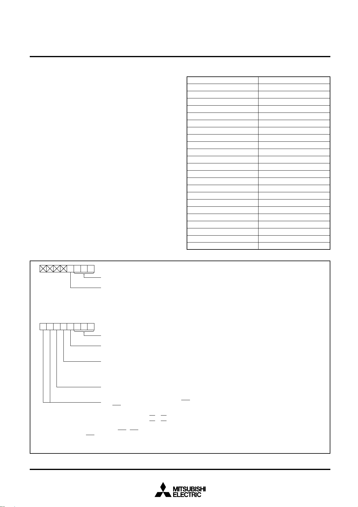
Address (Hexadecimal notation) Address (Hexadecimal notation)
000000
000001
000002
000003
000004
000005
000006
000007
000008
000009
00000A
00000B
00000C
00000D
00000E
00000F
000010
000011
000012
000013
000014
000015
000016
000017
000018
000019
00001A
00001B
00001C
00001D
00001E
00001F
000020
000021
000022
000023
000024
000025
000026
000027
000028
000029
00002A
00002B
00002C
00002D
00002E
00002F
000030
000031
000032
000033
000034
000035
000036
000037
000038
000039
00003A
00003B
00003C
00003D
00003E
00003F
Port P0 register
Port P1 register
Port P0 direction register
Port P1 direction register
Port P2 register
Port P3 register
Port P2 direction register
Port P3 direction register
Port P4 register
Port P5 register
Port P4 direction register
Port P5 direction register
Port P6 register
Port P7 register
Port P6 direction register
Port P7 direction register
Port P8 register
Port P9 register
Port P8 direction register
Port P9 direction register
Port P10 register
Port P11 register
Port P10 direction register
Port P11 direction register
Waveform output mode register
Dead-time timer
Pulse output data register 1
Pulse output data register 0
A-D control register 0
A-D control register 1
A-D register 0
A-D register 1
A-D register 2
A-D register 3
A-D register 4
A-D register 5
A-D register 6
A-D register 7
UART0 transmit/receive mode register
UART0 baud rate register
UART0 transmit buffer register
UART0 transmit/receive control register 0
UART0 transmit/receive control register 1
UART0 receive buffer register
UART1 transmit/receive mode register
UART1 baud rate register
UART1 transmit buffer register
UART1 transmit/receive control register 0
UART1 transmit/receive control register 1
UART1 receive buffer register
M37754S4CGP, M37754S4CHP
SINGLE-CHIP 16-BIT CMOS MICROCOMPUTER
000040
000041
000042
000043
000044
000045
000046
000047
000048
000049
00004A
00004B
00004C
00004D
00004E
00004F
000050
000051
000052
000053
000054
000055
000056
000057
000058
000059
00005A
00005B
00005C
00005D
00005E
00005F
000060
000061
000062
000063
000064
000065
000066
000067
000068
000069
00006A
00006B
00006C
00006D
00006E
00006F
000070
000071
000072
000073
000074
000075
000076
000077
000078
000079
00007A
00007B
00007C
00007D
00007E
00007F
Count start register
One-shot start register
Up-down register
Timer A write register
Timer A0 register
Timer A1 register
Timer A2 register
Timer A3 register
Timer A4 register
Timer B0 register
Timer B1 register
Timer B2 register
Timer A0 mode register
Timer A1 mode register
Timer A2 mode register
Timer A3 mode register
Timer A4 mode register
Timer B0 mode register
Timer B1 mode register
Timer B2 mode register
Processor mode register 0
Processor mode register 1
Watchdog timer register
Watchdog timer frequency select register
Chip select control register
Chip select area register
Comparator function select register
Reserved area (Note)
Comparator result register
Reserved area (Note)
D-A register 0
D-A register 1
Particular function select register 0
Particular function select register 1
INT4 interrupt control register
INT3 interrupt control register
A-D interrupt control register
UART0 trasmit interrupt control register
UART0 receive interrupt control register
UART1 trasmit interrupt control register
UART1 receive interrupt control register
Timer A0 interrupt control register
Timer A1 interrupt control register
Timer A2 interrupt control register
Timer A3 interrupt control register
Timer A4 interrupt control register
Timer B0 interrupt control register
Timer B1 interrupt control register
Timer B2 interrupt control register
INT0 interrupt control register
INT1 interrupt control register
INT2 interrupt control register
Fig. 2 Location of peripheral devices and interrupt control registers
8
Note: Do not write to this address.
MITSUBISHI MICROCOMPUTERS
M37754M8C-XXXGP, M37754M8C-XXXHP
PRELIMINARY
Notice: This is not a final specification.
Some parametric limits are subject to change.
CENTRAL PROCESSING UNIT (CPU)
The CPU has ten registers and is shown in Figure 3. Each of these
registers is described below.
ACCUMULATOR A (A)
Accumulator A is the main register of the microcomputer. It consists
of 16 bits and the low-order 8 bits can be used separately. The data
length flag m determines whether the register is used as 16-bit register or as 8-bit register. It is used as a 16-bit register when flag m is “0”
and as an 8-bit register when flag m is “1”. Flag m is a part of the processor status register (PS) which is described later.
Data operations such as calculations, data transfer, input/output,
etc., is executed mainly through the accumulator.
ACCUMULATOR B (B)
Accumulator B has the same functions as accumulator A, but the use
of accumulator B requires more instruction bytes and execution
cycles than accumulator A.
M37754S4CGP, M37754S4CHP
SINGLE-CHIP 16-BIT CMOS MICROCOMPUTER
In index addressing mode, register X is used as the index register
and the contents of this address is added to obtain the real address.
Index register X functions as a pointer register which indicates an
address of data table in instructions MVP, MVN, RMPA (Repeat
MultiPly and Accumulate).
INDEX REGISTER Y (Y)
Index register Y consists of 16 bits and the low-order 8 bits can be
used separately. The index register length flag x determines whether
the register is used as 16-bit register or as 8-bit register. It is used as
a 16-bit register when flag x is “0” and as an 8-bit register when flag x
is “1”. Flag x is a part of the processor status register (PS) which is
described later.
In index addressing mode, register Y is used as the index register
and the contents of this address is added to obtain the real address.
Index register Y functions as a pointer register which indicates an
address of data table in instructions MVP, MVN, RMPA (Repeat
MultiPly and Accumulate).
INDEX REGISTER X (X)
Index register X consists of 16 bits and the low-order 8 bits can be
used separately. The index register length flag x determines whether
the register is used as 16-bit register or as 8-bit register. It is used as
a 16-bit register when flag x is “0” and as an 8-bit register when flag
x is “1”. Flag x is a part of the processor status register (PS) which is
described later.
15 7 0
15 7 0
15
15 7 0
70
PG Program bank register PG
70
Data bank register DTDT
15 0
15 0
15 0
15
00000
AH AL Accumulator A
BH BL
XH XL
Y
H YL
IPL2 IPL1IPL0
7
S
PC
DPR
7
NVmxD I ZC
Accumulator B
0
Index register X
Index register Y
Stack pointer S
Program counter PC
Direct page register DPR
0
Processor status register PS
Carry flag
Zero flag
Interrupt disable flag
Decimal mode flag
Index register length flag
Data length flag
Overflow flag
Negative flag
Processor interrupt priority level IPL
Fig. 3 Register structure
9

MITSUBISHI MICROCOMPUTERS
M37754M8C-XXXGP, M37754M8C-XXXHP
PRELIMINARY
Notice: This is not a final specification.
Some parametric limits are subject to change.
STACK POINTER (S)
Stack pointer (S) is a 16-bit register. It is used during a subroutine call
or interrupts. It is also used during stack, stack pointer relative, or
stack pointer relative indirect indexed Y addressing mode.
PROGRAM COUNTER (PC)
Program counter (PC) is a 16-bit counter that indicates the low-order
16 bits of the next program memory address to be executed. There
is a bus interface unit between the program memory and the CPU,
so that the program memory is accessed through bus interface unit.
This is described later.
PROGRAM BANK REGISTER (PG)
Program bank register is an 8-bit register that indicates the high-order 8 bits of the next program memory address to be executed.
When a carry occurs by incrementing the contents of the program
counter, the contents of the program bank register (PG) is increased
by 1. Also, when a carry or borrow occurs after adding or subtracting
the offset value to or from the contents of the program counter (PC)
using the branch instruction, the contents of the program bank register (PG) is increased or decreased by 1, so that programs can be
written without worrying about bank boundaries.
DATA BANK REGISTER (DT)
Data bank register (DT) is an 8-bit register. With some addressing
modes, the data bank register (DT) is used to specify a part of the
memory address. The contents of data bank register (DT) is used as
the high-order 8 bits of a 24-bit address. Addressing modes that use
the data bank register (DT) are direct indirect, direct indexed X indirect, direct indirect indexed Y, absolute, absolute bit, absolute indexed X, absolute indexed Y, absolute bit relative, and stack pointer
relative indirect indexed Y.
DIRECT PAGE REGISTER (DPR)
Direct page register (DPR) is a 16-bit register. Its contents is used as
the base address of a 256-byte direct page area. The direct page
area is allocated in bank 0
FF01
16 or greater, the direct page area spans across bank 016 and
bank 1
16. All direct addressing modes use the contents of the direct
page register (DPR) to generate the data address. If the low-order 8
bits of the direct page register (DPR) is “00
required to generate an address is minimized.
Normally the low-order 8 bits of the direct page register (DPR) is set
to “00
16”.
16, but when the contents of DPR is
16”, the number of cycles
M37754S4CGP, M37754S4CHP
SINGLE-CHIP 16-BIT CMOS MICROCOMPUTER
PROCESSOR STATUS REGISTER (PS)
Processor status register (PS) is an 11-bit register. It consists of a
flag to indicate the result of operation and CPU interrupt levels.
Branch operations can be performed by testing the flags C, Z, V , and
N.
The details of each bit of the processor status register are described
below.
1. Carry flag (C)
The carry flag contains the carry or borrow generated by the ALU after an arithmetic operation. This flag is also affected by shift and rotate instructions. This flag can be set and reset directly with the SEC
and CLC instructions or with the SEP and CLP instructions.
2. Zero flag (Z)
The zero flag is set if the result of an arithmetic operation or data
transfer is zero and reset if it is not. This flag can be set and reset
directly with the SEP and CLP instructions.
3. Interrupt disable flag (I)
When the interrupt disable flag is set to “1”, all interrupts except
watchdog timer, DBC, and software interrupt are disabled. This flag
is set to “1” automatically when there is an interrupt. It can be set and
reset directly with the SEI and CLI instructions or SEP and CLP instructions.
4. Decimal mode flag (D)
The decimal mode flag determines whether addition and subtraction
are performed as binary or decimal. Binary arithmetic is performed
when this flag is “0”. If it is “1”, decimal arithmetic is performed with
each word treated as 2- or 4- digit decimal. Arithmetic operation is
performed using four digits when the data length flag m is “0” and
with two digits when it is “1”. Decimal adjust is automatically performed. (Decimal operation is possible only with the ADC and SBC
instructions.) This flag can be set and reset with the SEP and CLP
instructions.
___
10
MITSUBISHI MICROCOMPUTERS
M37754M8C-XXXGP, M37754M8C-XXXHP
PRELIMINARY
Notice: This is not a final specification.
Some parametric limits are subject to change.
5. Index register length flag (x)
The index register length flag determines whether index register X
and index register Y are used as 16-bit registers or as 8-bit registers.
The registers are used as 16-bit registers when flag x is “0” and as 8bit registers when it is “1”.
This flag can be set and reset with the SEP and CLP instructions.
6. Data length flag (m)
The data length flag determines whether the data length is 16-bit or
8-bit. The data length is 16-bit when flag m is “0” and 8-bit when it is
“1”. This flag can be set and reset with the SEM and CLM instructions
or with the SEP and CLP instructions.
7. Overflow flag (V)
The overflow flag is valid when addition or subtraction is performed
with a word treated as a signed binary number. If data length flag m
is “0”, the overflow flag is set when the result of addition or subtraction is outside the range between –32768 and +32767. If data length
flag m is “1”, the overflow flag is set when the result of addition or
subtraction is outside the range between –128 and +127. It is reset
in all other cases. The overflow flag can also be set and reset directly
with the SEP, and CLV or CLP instructions.
Additionally, the overflow flag is set when a result of unsigned/signed
division exceeds the length of the register where the result is to be
stored; the flag is also set when the addition result is outside range
of –2147483648 to +2147483647 in the RMPA operation.
8. Negative flag (N)
The negative flag is set when the result of arithmetic operation or
data transfer is negative (If data length flag m is “0”, data’s bit 15 is
“1”. If data length flag m is “1”, data’s bit 7 is “1”.) It is reset in all other
cases. It can also be set and reset with the SEP and CLP instructions.
M37754S4CGP, M37754S4CHP
SINGLE-CHIP 16-BIT CMOS MICROCOMPUTER
9. Processor interrupt priority level (IPL)
The processor interrupt priority level (IPL) consists of 3 bits and determines the priority of processor interrupts from level 0 to level 7.
Interrupt is enabled when the interrupt priority of the device requesting interrupt (set using the interrupt control register) is higher than the
processor interrupt priority. When interrupt is enabled, the current
processor interrupt priority level is saved in a stack and the processor interrupt priority level is replaced by the interrupt priority level of
the device requesting the interrupt. Refer to the section on interrupts
for more details.
Note: Fix bits 11 to 15 of the processor status register (PS) to “0”.
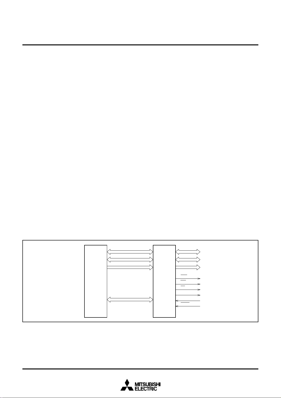
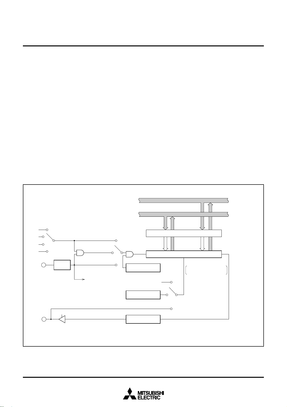
BUS INTERFACE UNIT
The CPU operates on the basis of internal clock φ CPU frequency. In
order to speed-up processing, a bus interface unit is used to prefetch instructions when the data bus is idle. The bus interface unit
synchronizes the CPU and the bus and pre-fetches instructions. Figure 4 shows the relationship between the CPU and the bus interface
unit.
The bus interface unit controls buses to access memories easily.
Refer to BUS CYCLE on the following pages. The bus interface unit
has a program address register, a 3-byte instruction queue buffer, a
data address register, and a 2-byte data buffer.
The bus interface unit obtains an instruction code from memory and
stores it in the instruction queue buffer, obtains data from memory
and stores it in the data buffer, or writes the data form the data buffer
to the memory.
D'8–D'15
D'
0–D'7
A'
0–A'23
CPU
Control signal
Fig. 4 Relationship between the CPU and the bus interface unit
Bus interface
unit
D8–D15
D0–D7
A0–A23
BHE
WR
RD
ALE
BYTE
HOLD
11
MITSUBISHI MICROCOMPUTERS
M37754M8C-XXXGP, M37754M8C-XXXHP
PRELIMINARY
Notice: This is not a final specification.
Some parametric limits are subject to change.
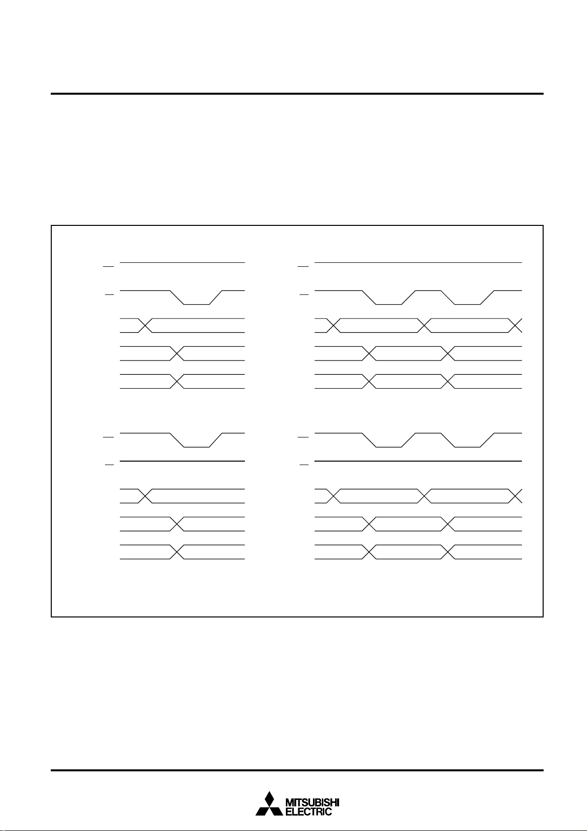
Figure 5 shows basic waveforms of the bus interface unit. The RD
signal becomes “L” when the bus interface unit reads an instruction
code or data from memory. The WR signal becomes “L” when the
___
bus interface unit writes data to memory.
Waveforms (1) and (3) in Figure 5 are used to access a single byte
or two bytes simultaneously. To read or write two bytes simultaneously, the first address accessed must be even. Furthermore,
when accessing an external memory area in memory expansion
mode or microprocessor mode, set the bus width select input pin
(1) (2)
WR
RD
Internal address
Internal data bus
0 – A23)
(A
(D
bus
0 – D7)
Address
Data (even)
__
Internal address
(A
Internal data bus
M37754S4CGP, M37754S4CHP
SINGLE-CHIP 16-BIT CMOS MICROCOMPUTER
(BYTE) to “L” (external data bus width = 16 bits). The internal
memory area is always treated as 16-bit bus width regardless of
BYTE.
When performing 16-bit data read or write, if the conditions for simultaneously accessing two bytes are not satisfied, waveforms (2) and
(4) are used to access each byte, one by one.
However, when prefetching the instruction code, if the address of the
instruction code is odd, only one byte is read in the instruction queue
buffer.
WR
RD
0 – A23)
(D
0 – D7)
bus
Address (odd) Address (even)
Invalid data
Data (even)
Internal data bus
(D
8 – D15)
Data (odd)
(3) (4)
WR
RD
Internal address
Internal data bus
Internal data bus
0 – A23)
(A
(D
(D
8 – D15)
bus
0 – D7)
Address
Data (even)
Data (odd)
Fig. 5 Basic waveforms of bus interface unit
Internal data bus
(D
8 – D15)
WR
RD
Internal address
Internal data bus
Internal data bus
0 – A23)
(A
(D
(D
8 – D15)
bus
0 – D7)
Data (odd)
Address (odd) Address (even)
Invalid data
Data (odd)
Invalid data
Data (even)
Invalid data
12

MITSUBISHI MICROCOMPUTERS
M37754M8C-XXXGP, M37754M8C-XXXHP
PRELIMINARY
Notice: This is not a final specification.
Some parametric limits are subject to change.
Instruction code read, data read, and data write are described below.
Instruction code read will be described first.
The CPU obtains instruction codes from the instruction queue buffer
and executes them. The CPU notifies the bus interface unit that CPU
is requesting an instruction code during an instruction code request
cycle. If the requested instruction code is not yet stored in the instruction queue buffer, the bus interface unit halts the CPU until it can
store more instructions than requested in the instruction queue
buffer.
Even if there is no instruction code request from the CPU, the bus
interface unit reads instruction codes from memory and stores them
in the instruction queue buffer when the instruction queue buffer is
empty or when only one instruction code is stored and the bus is idle
on the next cycle.
This is referred to as instruction pre-fetching.
Normally, when reading an instruction code from memory, if the accessed address is even, the next odd address is read together with
the instruction code and stored in the instruction queue buffer.
However , in memory expansion mode or microprocessor mode, if the
bus width select input (BYTE) is “H” and external data bus width is 8
bits, and if the address to be read is in external memory area or is
odd, only one byte is read and stored in the instruction queue buffer.
Data read and write are described below.
The CPU notifies the bus interface unit when performing data read
or write. At this time, the bus interface unit halts the CPU if the bus
interface unit is already using the bus or if there is a request with
higher priority. When data read or write is enabled, the bus interface
unit performs data read or write.
During data read, the CPU waits until the entire data is stored in the
data buffer. The bus interface unit sends the address sent from the
___
M37754S4CGP, M37754S4CHP
SINGLE-CHIP 16-BIT CMOS MICROCOMPUTER
13

MITSUBISHI MICROCOMPUTERS
φ
RD
WR
A
i
Di
φ
A
iADRS ADRS
W-D
1bus cycle = 3φ1bus cycle = 3φ
D
i
RD
WR
Read Write
R-D
φ
RD
WR
A
i
Di
φ
A
iADRS ADRS
W-DR-D
1bus cycle = 2φ1bus cycle = 2φ
D
i
RD
WR
Read Write
φ
A
i
ADRS ADRS
W-DR-D
1bus cycle = 4φ1bus cycle = 4φ
D
i
RD
WR
φ
A
i
Di
RD
WR
Read
Write
M37754M8C-XXXGP, M37754M8C-XXXHP
PRELIMINARY
Notice: This is not a final specification.
Some parametric limits are subject to change.
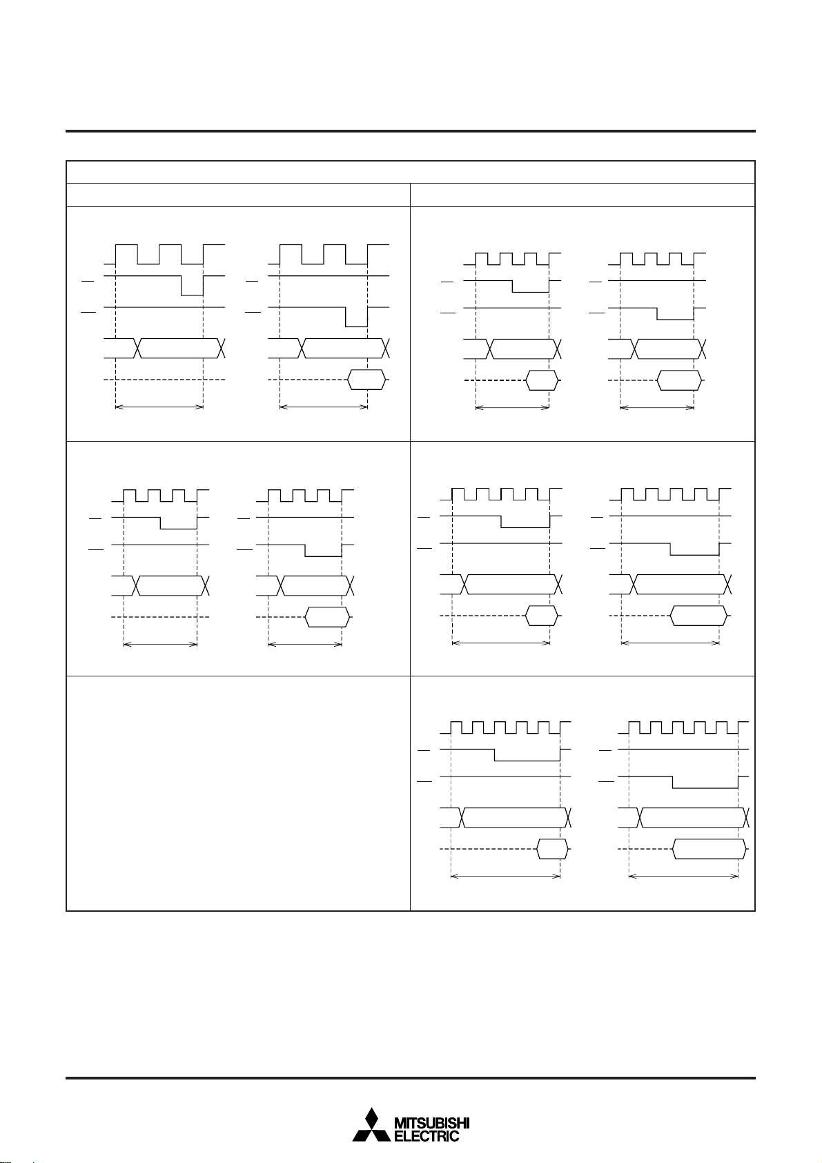
Internal memory access External memory access
2-φ access
Read Write
φ
RD
WR
i
A
Di
Low-speed running (
φ
RD
WR
iADRS ADRS
A
i
D
1bus cycle = 2φ1bus cycle = 2φ
W-D
M37754S4CGP, M37754S4CHP
SINGLE-CHIP 16-BIT CMOS MICROCOMPUTER
φ
1 ≤ 12.5 MHZ)
2-φ access
3-
φ
access
––––––––––––––––––––––––––––––
∗ADRS: Address
R-D : Read data
W-D : Write data
Fig. 6 Bus cycle selection (low-speed running)
4-φ access
14
MITSUBISHI MICROCOMPUTERS
φ
RD
WR
A
i
Di
φ
A
iADRS ADRS
W-DR-D
1bus cycle = 5φ1bus cycle = 5φ
D
i
RD
WR
Read Write
φ
RD
WR
A
i
Di
φ
A
iADRS ADRS
W-DR-D
1bus cycle = 4φ1bus cycle = 4φ
D
i
RD
WR
Read Write
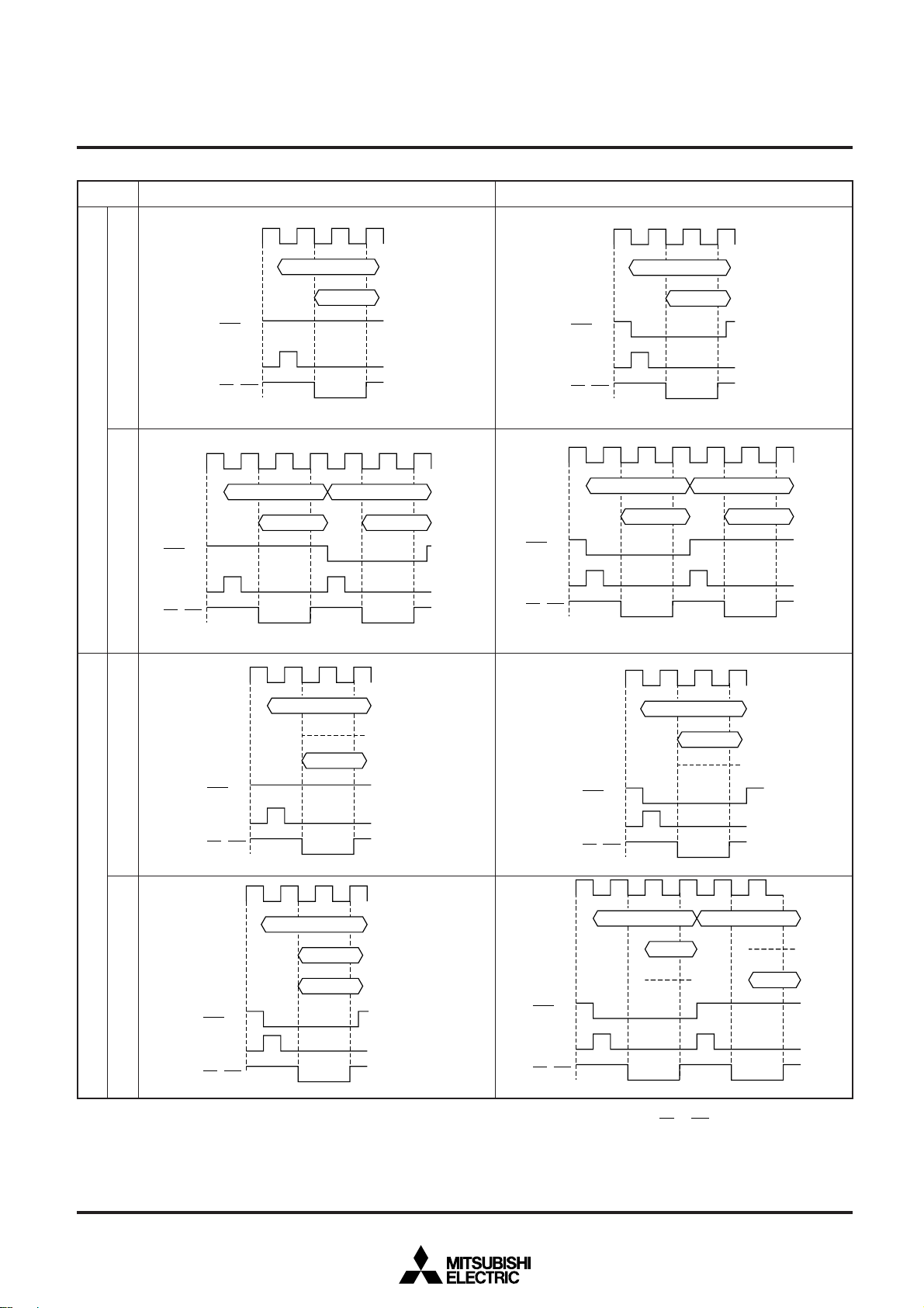
M37754M8C-XXXGP, M37754M8C-XXXHP
PRELIMINARY
Notice: This is not a final specification.
Some parametric limits are subject to change.
Internal memory access External memory access
2-φ access (Note)
Read Write
φ
RD
WR
i
A
Di
3-φ access (Note)
Read Write
High-speed running (
φ
RD
WR
iADRS ADRS
A
i
D
1bus cycle = 2φ1bus cycle = 2φ
W-D
M37754S4CGP, M37754S4CHP
SINGLE-CHIP 16-BIT CMOS MICROCOMPUTER
φ
1 ≤ 20 MHZ)
3-φ access
Read Write
4-
φ
φ
RD
WR
i
A
Di
access
R-D
φ
RD
WR
iADRS ADRS
A
i
D
1bus cycle = 3φ1bus cycle = 3φ
W-D
φ
RD
WR
A
Di
i
φ
RD
WR
iADRS ADRS
A
i
D
1bus cycle = 3φ1bus cycle = 3φ
W-D
Note: Refer to internal memory access bus cycle select bit (bit 2
of processor mode register 0 ; Figure 14).
∗ADRS: Address
R-D : Read data
W-D : Write data
5-φ access
Fig. 7 Bus cycle selection (high-speed running)
15
Y
φ1
Ai A0 – A23
Di D0 – D7
A0 – A23
D0 – D7
BHE
RD, WR
ALE
φ1
DHi
(Note 1)
A
i
BHE
A
0 – A23
DLi
D8 – D15
RD, WR
ALE
φ1
DHi
(Note 1)
(Note 1)
A
i
BHE
A
0 – A23 A0 – A23
DLi
D8 – D15
D0 – D7
RD, WR
ALE
MITSUBISHI MICROCOMPUTERS
M37754M8C-XXXGP, M37754M8C-XXXHP
PRELIMINAR
Notice: This is not a final specification.
Some parametric limits are subject to change.
Access from even address Access from odd address
φ1
Ai A0 – A23
Di D0 – D7
BHE
1-byte Read/Write
φ1
Ai A0 – A23
External data bus width = 8 bits
Di D0 – D7
ALE
RD, WR
M37754S4CGP, M37754S4CHP
SINGLE-CHIP 16-BIT CMOS MICROCOMPUTER
φ1
Ai A0 – A23
Di D0 – D7
BHE
ALE
RD, WR
A0 – A23
D0 – D7
BHE
ALE
2-byte Read/Write
RD, WR
φ1
A
i
DHi
DLi
BHE
1-byte Read/Write
External data bus width = 16 bits
ALE
RD, WR
φ1
Ai
DHi
DLi
A
0 – A19
(Note 1)
0 – A23
A
D8 – D15
D0 – D7
D0 – D7
2-byte Read/Write
Notes 1: It becomes Hi-Z when reading, and it outputs undefined data when writing.
2: When the external data bus width is 8 bits, the function to output the low-order address from the Di pin while RD or WR is “H” can be selected only
in special area access cycle. Refer to the section on the processor mode for details.
Fig. 8 Output signals at 3-φ access in high-speed running
16
BHE
ALE
RD, WR
MITSUBISHI MICROCOMPUTERS
M37754M8C-XXXGP, M37754M8C-XXXHP
PRELIMINARY
Notice: This is not a final specification.
Some parametric limits are subject to change.
76543210
0 0 0 Processor mode register 1 5F
M37754S4CGP, M37754S4CHP
SINGLE-CHIP 16-BIT CMOS MICROCOMPUTER
Address
16
These bits must be “00.”
Clock source for peripheral devices select bit (Note)
1/2
0 : φ
1
1 :φ
CPU running speed select bit
0 : High-speed running
1 : Low-speed running
Bus cycle select bits
In high-speed running
00 : 5-φ access in high-speed running
01 : 4-φ access in high-speed running
10 : 3-φ access in high-speed running
11 : Do not select.
In low-speed running
00 : Do not select.
01 : 4-φ access in low-speed running
10 : 3-φ access in low-speed running
11 : 2-φ access in low-speed running
Note: When φ1 > 12.5 MHz, set bit 2 to “0.”
Fig. 9 Processor mode register 1 bit configuration
Clock source select bit
1 = f(XIN)/2
0 : φ
1 = f(XIN)
1 : φ
This bit must be “0.”
17
MITSUBISHI MICROCOMPUTERS
M37754M8C-XXXGP, M37754M8C-XXXHP
PRELIMINARY
Notice: This is not a final specification.
Some parametric limits are subject to change.
INTERRUPTS
Table 2 shows the interrupt types and the corresponding interrupt
vector addresses. Reset is also treated as a type of interrupt and is
discussed in this section, too.
___
DBC is an interrupt used during debugging.
Interrupts other than reset, DBC, watchdog timer, zero divide, and
BRK instruction all have interrupt control registers. Table 3 shows the
addresses of the interrupt control registers and Figure 10 shows the
bit configuration of the interrupt control register.
The interrupt request bit is automatically cleared by the hardware
during reset or when processing an interrupt. Also, interrupt request
bits other than DBC and watchdog timer can be cleared by software.
____ ___
INT4 to INT0 are external interrupts; whether to cause an interrupt at
___
the input level (level sense) or at the edge (edge sense) can be selected with the level/edge select bit. Furthermore, the polarity of the
interrupt input can be selected with the polarity select bit.
___ ___ __ __ __
In the INT3 external interrupt, the INT3 input, KI3 to KI0 inputs, or KI4
__
to KI0 inputs can be selected with bits 7 and 6 of INT3 interrupt control register.
Timer and UART interrupts are described in the respective section.
The priority of interrupts when multiple interrupts are caused simultaneously is partially fixed by hardware, but, it can also be adjusted
by software as shown in Figure 11.
The hardware priority is fixed as the following:
___
reset > DBC > watchdog timer > other interrupts
___
____
M37754S4CGP, M37754S4CHP
SINGLE-CHIP 16-BIT CMOS MICROCOMPUTER
Table 2. Interrupt types and the interrupt vector addresses
____
INT4 external interrupt
____
INT3 external interrupt
Interrupts
A-D
UART1 transmit
UART1 receive
UART0 transmit
UART0 receive
Timer B2
Timer B1
Timer B0
Timer A4
Timer A3
Timer A2
Timer A1
Timer A0
____
INT2 external interrupt
____
INT1 external interrupt
____
INT0 external interrupt
Watchdog timer
____
DBC (Do not select.)
Break instruction
Zero divide
Reset
Vector addresses
00FFD216 00FFD316
00FFD416 00FFD516
00FFD616 00FFD716
00FFD816 00FFD916
00FFDA16 00FFDB16
00FFDC16 00FFDD16
00FFDE16 00FFDF16
00FFE016 00FFE116
00FFE216 00FFE316
00FFE416 00FFE516
00FFE616 00FFE716
00FFE816 00FFE916
00FFEA16 00FFEB16
00FFEC16 00FFED16
00FFEE16 00FFEF16
00FFF016 00FFF116
00FFF216 00FFF316
00FFF416 00FFF516
00FFF616 00FFF716
00FFF816 00FFF916
00FFFA16 00FFFB16
00FFFC16 00FFFD16
00FFFE16 00FFFF16
76543210
Interrupt priority level
Interrupt request bit (Note 1)
0 : No interrupt
1 : Interrupt
Interrupt control register configuration for A-D converter, UART0, UART1, timer A0 to timer A4, and timer B0 to timer B2.
Note 1: The A-D conversion interrupt request bit becomes undefined after reset. Clear this bit to “0” before use of the A-D conversion interrupt.
76543210
Interrupt priority level
Interrupt request bit
0 : No interrupt
1 : Interrupt
Polarity select bit
0 : Set interrupt request bit at “H” level for level sense and when changing from “H” to “L”
level for edge sense.
1 : Set interrupt request bit at “L” level for level sense and when changing from “L” to “H”
level for edge sense.
Level/Edge select bit
0 : Edge sense
1 : Level sense
Key input interrupt select bits 1, 0 (only for INT
0 0 : INT
3 interrupt selected
0 1 : Do not select.
1 0 : Key input interrupt (KI
1 1 : Key input interrupt (KI
Interrupt control register configuration for INT4– INT0 (Note 2).
Note 2: The contents of INT
Figure 15) is set to “1.”
4 interrupt control register after reset cannot be changed unless bit 5 of the particular function select register 1 (see
3 to KI0) selected
4 to KI0) selected
3 interrupt control register)
Fig. 10 Interrupt control register bit configuration
18

MITSUBISHI MICROCOMPUTERS
M37754M8C-XXXGP, M37754M8C-XXXHP
PRELIMINARY
Notice: This is not a final specification.
Some parametric limits are subject to change.
Table 3. Addresses of interrupt control registers
____
____
____
____
____
Interrupt control registers
INT4 interrupt control register
INT3 interrupt control register
A-D interrupt control register
UART0 transmit interrupt control register
UART0 receive interrupt control register
UART1 transmit interrupt control register
UART1 receive interrupt control register
Timer A0 interrupt control register
Timer A1 interrupt control register
Timer A2 interrupt control register
Timer A3 interrupt control register
Timer A4 interrupt control register
Timer B0 interrupt control register
Timer B1 interrupt control register
Timer B2 interrupt control register
INT0 interrupt control register
INT1 interrupt control register
INT2 interrupt control register
Addresses
00006E16
00006F16
00007016
00007116
00007216
00007316
00007416
00007516
00007616
00007716
00007816
00007916
00007A16
00007B16
00007C16
00007D16
00007E16
00007F16
M37754S4CGP, M37754S4CHP
SINGLE-CHIP 16-BIT CMOS MICROCOMPUTER
The interrupt request bit and the interrupt priority level of each interrupt source are sampled and latched at each operation code fetch
cycle while
until the cycles whose number is selected by software has passed,
even if the next operation code fetch cycle is generated. The detection of an interrupt which has the highest priority is performed during
that time.
A-D converter, UART, etc. interrupts
Priority can be changed with software inside 4
Fig. 11 Interrupt priority
φ
BIU is “H”. However, no sampling pulse is generated
Priority is determined by hardware
4
321
Watchdog
timer
DBC
Reset
Interrupts caused by a BRK instruction and when dividing by zero are
software interrupts and are not included in this list.
Other interrupts previously mentioned are A-D converter, UART, etc.
interrupts. The priority of these interrupts can be changed by changing the priority level in the corresponding interrupt control register by
software.
Figure 12 shows a diagram of the interrupt priority detection circuit
When an interrupt is caused, each interrupt device compares its own
priority with the priority from above and if its own priority is higher,
then it sends the priority below and requests the interrupt. If the priorities are the same, the one above has priority.
This comparison is repeated to select the interrupt with the highest
priority among the interrupts that are being requested. Finally the
selected interrupt is compared with the processor interrupt priority
level (IPL) contained in the processor status register (PS) and the
request is accepted if it is higher than IPL and the interrupt disable
flag I is “0”. The request is not accepted if flag I is “1”. The reset, DBC,
___
and watchdog timer interrupts are not affected by the interrupt disable flag I.
When an interrupt is accepted, the contents of the processor status
register (PS) is saved to the stack and the interrupt disable flag I is
set to “1”.
Furthermore, the interrupt request bit of the accepted interrupt is
cleared to “0” and the processor interrupt priority level (IPL) in the
processor status register (PS) is replaced by the priority level of the
accepted interrupt.
Therefore, multi-level priority interrupts are possible by resetting the
interrupt disable flag I to “0” and enable further interrupts.
For reset, DBC, watchdog timer, zero divide, and BRK instruction in-
___
terrupts, which do not have an interrupt control register, the processor interrupt level (IPL) is set as shown in Table 4.
Reset
DBC
Watchdog timer
Interrupt disable flag I
IPL
Interrupt request
INT
4
INT
3
A-D
UART1 transmit
UART1 receive
UART0 transmit
UART0 receive
Timer B2
Timer B1
Timer B0
Timer A4
Timer A3
Timer A2
Timer A1
Timer A0
INT
2
INT
2
INT
1
INT
1
INT
0
Level 0
Fig. 12 Interrupt priority detection
19
MITSUBISHI MICROCOMPUTERS
M37754M8C-XXXGP, M37754M8C-XXXHP
PRELIMINARY
Notice: This is not a final specification.
Some parametric limits are subject to change.
As shown in Figure 13, there are three different interrupt priority detection time from which one is selected by software. After the selected time has elapsed, the highest priority is determined and is
processed after the currently executing instruction has been completed.
The time is selected with bits 4 and 5 of the processor mode register
0 (address 5E
between these bits and the number of cycles. After a reset, the processor mode register 0 is initialized to “00
time is automatically set, however, the shortest time must be selected by software.
16) shown in Figure 14. Table 5 shows the relationship
16.” Therefore, the longest
BIU
φ
M37754S4CGP, M37754S4CHP
SINGLE-CHIP 16-BIT CMOS MICROCOMPUTER
Table 4.
V alue set in processor interrupt level (IPL) during an interr upt
Interrupt types
Reset
____
DBC
Watchdog timer
Zero divide
BRK instruction
Table 5. Relationship between interrupt priority detection time select
bit and number of cycles
Priority detection time select bit
Bit 5
0
0
1
Bit 4
0
1
0
Setting value
0
7
7
Not change value of IPL.
Not change value of IPL.
Number of cycles
7 cycles of
4 cycles of
2 cycles of
φ
BIU
φ
BIU
φ
BIU
Operation code fetch cycle
Sampling pulse
Priority detection time
Select one from 0 to 2 with
bits 4 and 5 of processor
mode register 0
Fig. 13 Interrupt priority detection time
0
1
2
20
MITSUBISHI MICROCOMPUTERS
M37754M8C-XXXGP, M37754M8C-XXXHP
PRELIMINARY
Notice: This is not a final specification.
Some parametric limits are subject to change.
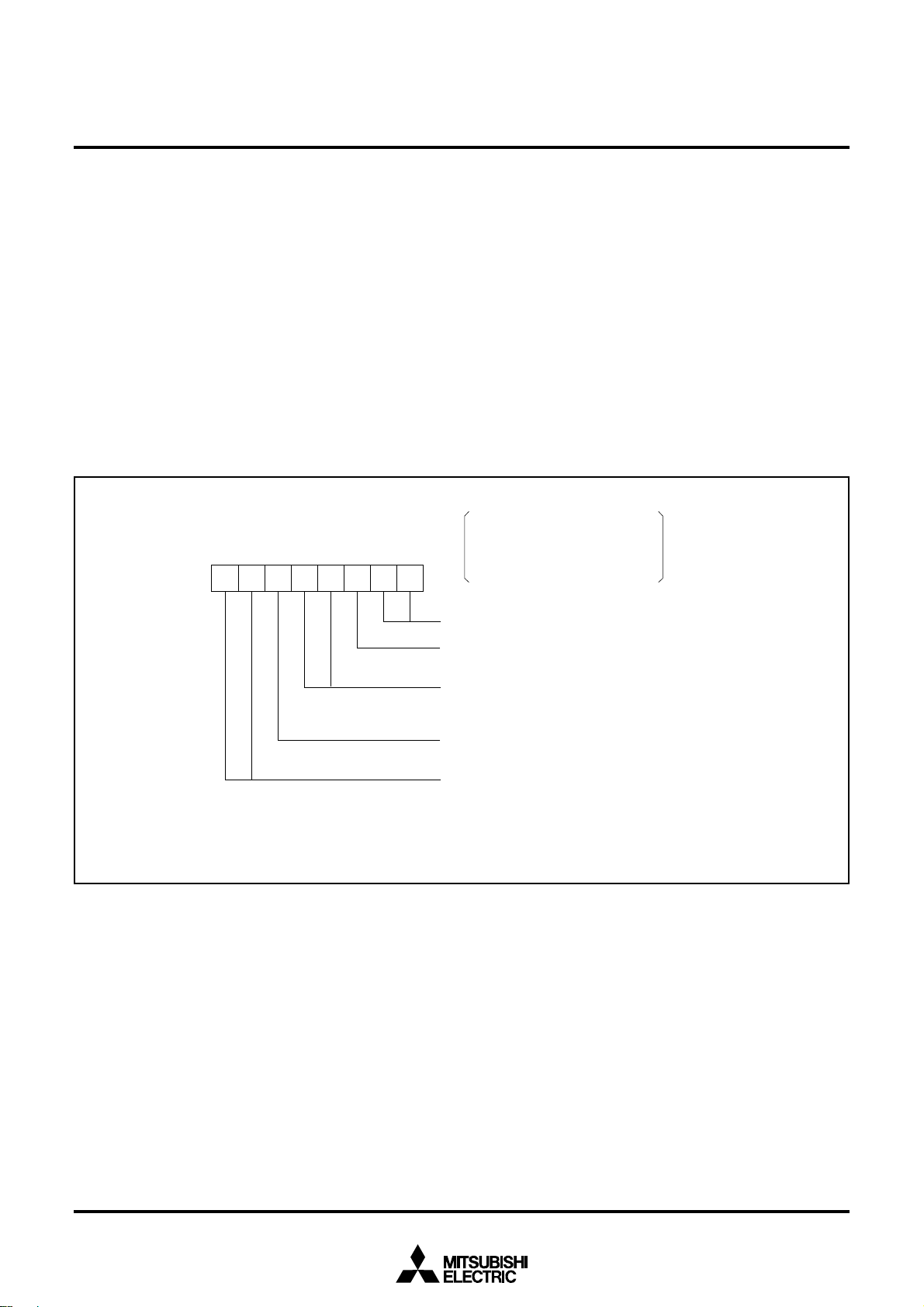
76543210
0 Processor mode register 0 (5E16)
M37754S4CGP, M37754S4CHP
SINGLE-CHIP 16-BIT CMOS MICROCOMPUTER
Processor mode bits
00 : Single-chip mode
01 : Memory expansion mode
10 : Microprocessor mode
11 : Do not select.
Internal memory access bus cycle select bit (Note)
Internal memory access condition in high-speed running
0 : 2-φ access for internal RAM, 3-φ access for internal ROM and SFR
1 : 2-φ access for internal RAM, internal ROM, SFR
Software reset bit
The microcomputer is reset when this bit is set to “1”.
Interrupt priority detection time select bit
0 0 : Select 0 in Figure 13
0 1 : Select 1 in Figure 13
1 0 : Select 2 in Figure 13
Test mode bit
This bit must be “0.”
Clock φ
1 output select bit
0 : No φ
1 output
1 : φ
1 output
Note: When selecting low-speed running, set bit 2 to “0.”
Fig. 14 Processor mode register 0 bit configuration
76543210
TC1
Particular function select register 1 (6D
TC0
Transmit clock output pin select bit
00 : Normal mode (output only to CLK
01 : Plural clocks specified; output to CLK
10 : Plural clocks specified; output to CLKS0
11 : Plural clocks specified; output to CLKS1
Internal clock stop select bit at WIT (Note 1)
0 : Clock for peripheral function and watchdog timer are operating at WIT
1 : Internal clock except that for oscillation circuit and watchdog timer are stopped at WIT
Watchdog timer’s clock select bit (Note 1)
0 : Exclusive clock deviding circuit output (Wf
timer. Clock (Wf
1 : Clock for peripheral device deviding circuit output (Pf
watchdog timer. Clock (Pf
Watchdog timer exclusive clock dividing circuit is stopped.
Signal output stop select bit (Note 1)
Refer to Table 8.
Expansion function select bit (Note 2)
Refer to Figure 62.
Pull-up select bit 0 (Note 3)
0 : With no pull-up for P5
1 : With pull-up for P57, P56, P55, P54
Pull-up select bit 1 (Note 3)
0 : With no pull-up for P9
1 : With pull-up for P95
16)
0)
0
512, Wf32) is used as clock for watchdog
512, Wf32) for watchdog timer does not change in hold.
512, Pf32) is used as clock for
512, Pf32) for watchdog timer changes in hold.
7, P56, P55, P54
5
Notes 1: Bits 2, 3, and 4 can be re-write after bit 5 (expansion function select bit) is set to “1.”
2: After bit 5 is set to “1” once, bit 5 cannot be cleared to “0” except external reset and software reset.
3:
Bits 6 and 7 are write-only bits and undefined at read. Do not use SEB or CLB insturuction when setting bits 0–7.
Fig. 15 Processor mode register 0 bit configuration
21
MITSUBISHI MICROCOMPUTERS
M37754M8C-XXXGP, M37754M8C-XXXHP
PRELIMINARY
Notice: This is not a final specification.
Some parametric limits are subject to change.
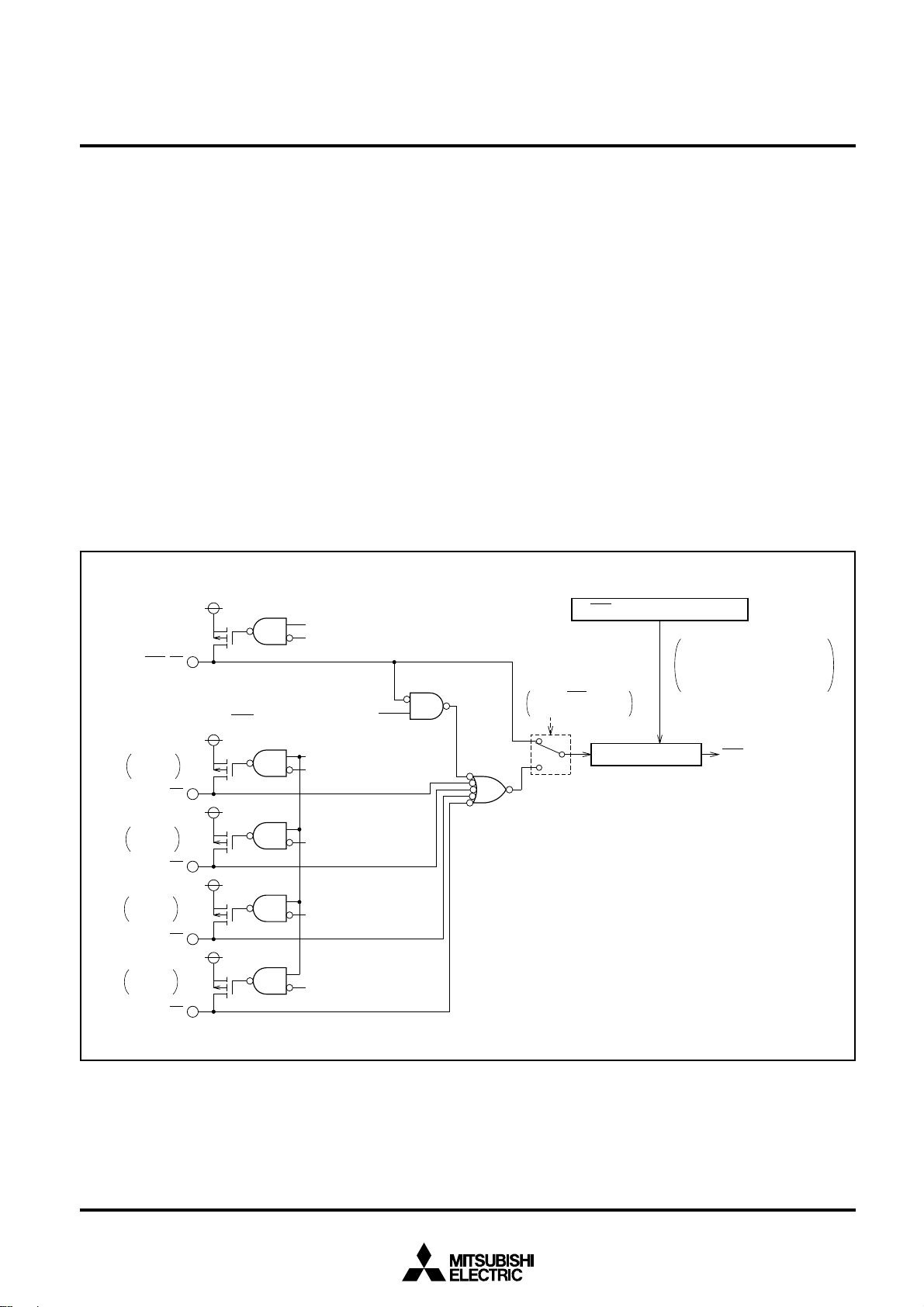
___
The INT3 interrupt can function as the key input interrupt by setting
bits 7 and 6 of the INT3 interrupt control register. The key input interrupt uses inputs KI3 to KI0 or inputs KI4 to KI0. Figure 10 shows the
interrupt control register bit configuration. Figure 15 shows the particular function select register 1 bit configuration, and Figure 16
shows the INT3/key input interrupt input circuit block diagram.
When the INT3 interrupt control register’s bit 7 is “0” and its bit 6 is
“0”, a signal from the INT3 pin is connected to the INT3 interrupt control circuit and INT3 external interrupt is normally performed.
When the INT3 interrupt control register’s bit 7 is “1” and its bit 6 is
“0”, signals from the KI3 to KI0 pins, which correspond to ports P57 to
P5
4, are inverted and then the logical sum of these signals is con-
nected to the INT3 interrupt control circuit. In this case, the external
interrupt which uses the KI3 to KI0 pins is performed.
When the INT3 interrupt control register’s bit 7 is “1” and its bit 6 is
“1”, signals from the KI4 pin, which corresponds to port P95, KI3 to
__
KI0 pins, which correspond to ports P57 to P54, are inverted and then
the logical sum of these signals is connected to the INT3 interrupt
control circuit. In this case, the external interrupt which uses the KI4
___
__ __ __ __
___
___
___ ___
___
___
__ __
___
__ __
___
__ __
___
__
M37754S4CGP, M37754S4CHP
SINGLE-CHIP 16-BIT CMOS MICROCOMPUTER
__
to KI0 pins is performed.
When using the above key input interrupt, select the edge sense
which uses the falling edge from “H” to “L” with the INT3 interrupt
control register so that an interrupt request can occur by inputting “L”
to each of the KI3 to KI0 pins or the KI4 to KI0 pins. The interrupt vector is common to the INT3 interrupt’s one. Additionally, pull-up resistor (transistors) can be added to the KI4 to KI0 pins by setting the
__ __ __ __
___
__ __
contents of the particular function select register 1’s bits 7 and 6 and
setting “0” to each bit of the corresponding port’s direction register.
___
P95/INT3/KI4
Pull-up
transistor
7/TA3IN/KI3
P5
Pull-up
transistor
P56/TA3OUT/KI2
Pull-up
transistor
P55/TA2IN/KI1
Pull-up
transistor
P54/TA2OUT/KI0
Key input interrupt select bit 0
(Bit 6 of INT
3 interrupt control register)
Pull-up select bit 1
Port P95 direction register
Pull-up select bit 0
Port P5
7 direction
register
Port P5
6 direction
register
Port P5
5 direction
register
Port P5
4 direction
register
INT3 interrupt control register (Address 6F16)
Key input interrupt select bit 1
Bit 7 of INT3 interrupt
control register
0
Interrupt control circuit
1
When the key input interrupt
is selected, select the edge
sense which uses falling edge
from “H” to “L”.
INT3 interrupt request
___
Fig. 16 INT3/key input interrupt input circuit block diagram
22
MITSUBISHI MICROCOMPUTERS
M37754M8C-XXXGP, M37754M8C-XXXHP
PRELIMINARY
Notice: This is not a final specification.
Some parametric limits are subject to change.
TIMER
There are eight 16-bit timers. They are divided by type into timer A(5)
and timer B(3).
The timer I/O pins are multiplexed with I/O pins for port P5 and P6.
To use these pins as timer input pins, the data direction register bit
corresponding to the pin must be cleared to “0” to specify input mode.
TIMER A
Figure 17 shows a block diagram of timer A.
Timer A has four modes: timer mode, event counter mode, one-shot
pulse mode, and pulse width modulation mode. The mode is selected with bits 0 and 1 of the timer Ai mode register (i = 0 to 4). Each
of these modes is described below.
M37754S4CGP, M37754S4CHP
SINGLE-CHIP 16-BIT CMOS MICROCOMPUTER
(1) Timer mode [00]
Figure 18 shows the bit configuration of the timer Ai mode register
during timer mode. Bits 0 and 1 of the timer Ai mode register must be
“0” in timer mode. Bits 3, 4, and 5 are used to select the gate function. Bits 4 and 5 must be “0” when not selecting the gate function.
Bit 3 is ignored if bit 4 is “0”.
Bits 6 and 7 are used to select the timer counter source.
The counting of the selected clock starts when the count start bit is
“1” and stops when it is “0”.
Figure 19 shows the bit configuration of the count start bit. The
counter is decremented, an interrupt is caused and the interrupt request bit in the timer Ai interrupt control register is set when the contents becomes 0000
register is transferred to the counter and count is continued.
When data is written to timer Ai register with timer Ai halted, the same
data is also written to the reload register and the counter. When data
is written to timer Ai which is busy, the data is written to the reload
register, but not to the counter . The new data is reloaded from the reload register to the counter at the next reload time and counting continues. The contents of the counter can be read at any time.
When the value set in the timer Ai register is n, the timer frequency
dividing ratio is 1/(n+1).
16. At the same time, the contents of the reload
Clock source selection
2
Pf
Pf
16
Pf
64
Pf
512
Polarity
selection
IN
TAi
(i = 0–4)
Pulse output
TAi
OUT
(i = 0–4)
• Timer
• One-shot
• Pulse width modulation
Timer(gate function)
Event counter
External trigger
Count start bit
(40
16
)
Down count
Up-down bit
(44
16
)
Toggle flip-flop
Data bus (odd)
Data bus (even)
(Lower 8 bits) (Higher 8 bits)
Reload register(16)
Counter(16)
Up/Down
Always decremented
except in event count mode
A
ddresses
16
Timer A0 47
Timer A1 4916 48
Timer A2 4B16 4A
Timer A3 4D16 4C
Timer A4 4F16 4E
46
16
16
16
16
16
Note: Perform write and read to/from timer Ai register in the condition of 16-bit data length : data length flag (m) = “0”.
Fig. 17 Block diagram of timer A
23
MITSUBISHI MICROCOMPUTERS
M37754M8C-XXXGP, M37754M8C-XXXHP
PRELIMINARY
Notice: This is not a final specification.
Some parametric limits are subject to change.
Pulse output function
When bit 2 of the timer Ai mode register is “1”, the output is generated from TAi
the counter reaches to 0000
bit is “0”, “L” is output from TAi
When bit 2 is “0”, TAi
4 is “0”, TAi
Gate function
When bit 4 is “1”, counting is performed only while the input signal
from the TAi
can be used to measure the pulse width of the TAi
Whether to count while the input signal is “H” or while it is “L” is determined by bit 3. If bit 3 is “1”, counting is performed while the TAi
pin input signal is “H” and if bit 3 is “0”, counting is performed while it
is “L”.
OUT pin. The output is toggled each time the contents of
16. When the contents of the count start
OUT pin.
OUT can be used as a normal port pin. When bit
IN can be used as a normal port pin.
IN pin is “H” or “L” as shown in Figure 20. Therefore, this
IN input signal.
7
6543210
00
M37754S4CGP, M37754S4CHP
SINGLE-CHIP 16-BIT CMOS MICROCOMPUTER
When bit 5 is “0, counting restarts from the value which is contained
at restarting (gate function 0 [no reload]) and an overflow occurs (n +
1) cycles of the count source later. Figure 21 shows that operation.
When bit 5 is “1”, counting restarts from the value which is obtained
by reload at restarting (gate function 1 [reload]) and the first overflow
occurs (n + 2) cycles of the count source later. Figure 22 shows that
operation. After that, while the input signal from the TAi
valid level, an overflow occurs at (n + 1)- cycle intervals. Make sure
to set the value of 1 or more to n.
When gate functions are used, the duration of “H” or “L” on the TAi
pin must be 2 or more cycles of the timer count source.
IN
Timer A0 mode register
Timer A1 mode register
Timer A2 mode register
Timer A3 mode register
Timer A4 mode register
Addresses
56
16
5716
58
16
59
16
5A
16
IN pin keeps
IN
Note: When selecting no gate function (bit 4 = “0”) in timer mode, fix bit 5 to “0”.
Fig. 18 Timer Ai mode register bit configuration during timer mode
0 0 : Always “00” in timer mode
0 : No pulse output (TAi
1 : Pulse output
0
×
: No gate function (TAiIN is normal port pin)
1 0 : Count only while TAi
1 1 : Count only while TAi
0 : Gate function 0 (No reload)
1 : Gate function 1 (Reload) ; Note
Clock source select bit
0 0 : Select Pf
0 1 : Select Pf
1 0 : Select Pf
1 1 : Select Pf
2
16
64
512
OUT
is normal port pin)
IN
input is “L”
IN
input is “H”
24
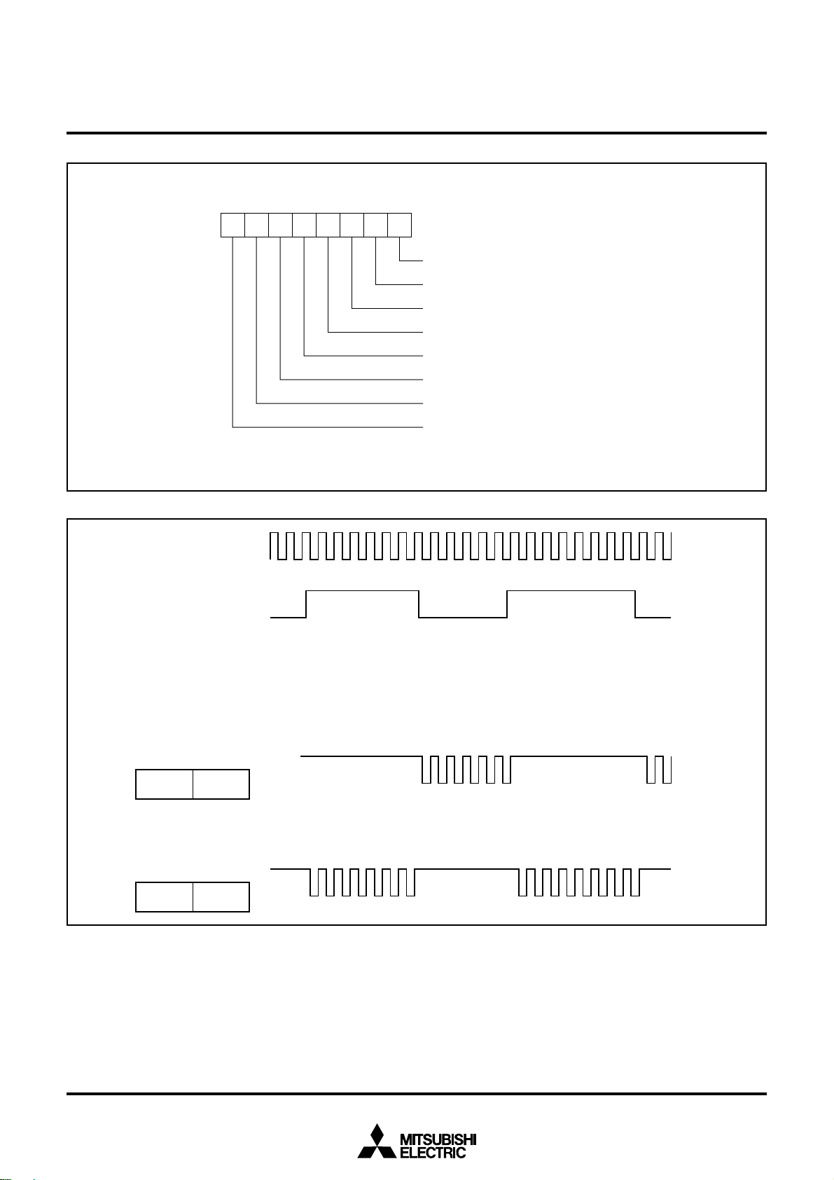
MITSUBISHI MICROCOMPUTERS
M37754M8C-XXXGP, M37754M8C-XXXHP
PRELIMINARY
Notice: This is not a final specification.
Some parametric limits are subject to change.
76543210
M37754S4CGP, M37754S4CHP
SINGLE-CHIP 16-BIT CMOS MICROCOMPUTER
Count start register
(Stop at “0”, Start at “1”)
Timer A0 count start bit
Timer A1 count start bit
Timer A2 count start bit
Timer A3 count start bit
Timer A4 count start bit
Timer B0 count start bit
Timer B1 count start bit
Timer B2 count start bit
Address
40
16
Fig. 19 Count start flag bit configuration
Selected clock source Pfi
TAi
IN
Timer mode register
Bit 4 Bit 3
10
Timer mode register
Bit 4 Bit 3
11
Fig. 20 Count waveform when gate function is available
25
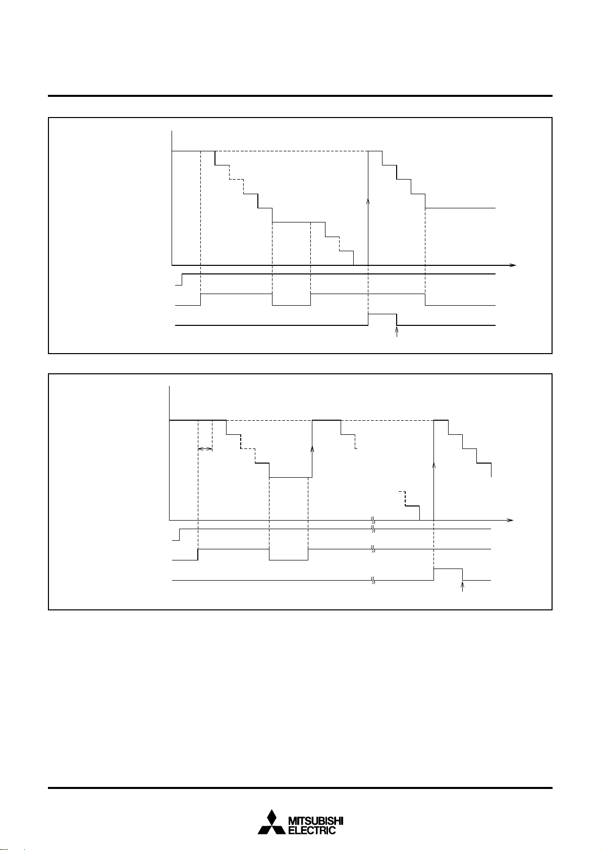
MITSUBISHI MICROCOMPUTERS
M37754M8C-XXXGP, M37754M8C-XXXHP
PRELIMINARY
Notice: This is not a final specification.
Some parametric limits are subject to change.
FFFF
16
n
Count start flag
Input level to
TAi
IN pin
TAi interrupt
request bit
“1”
“0”
Valid level
Invalid level
Count start
Count stop
M37754S4CGP, M37754S4CHP
SINGLE-CHIP 16-BIT CMOS MICROCOMPUTER
Count stop
Overflow
Time
Cleared by accepting the interrupt request or by software
Fig. 21 Timer operation example with gate function 0 (no reload) selected
FFFF
16
Count start flag
Input level to
TAi
IN pin
TAi interrupt
request bit
n
“1”
“0”
Valid level
Invalid level
Count start
Reloaded
duration
Reloaded
Count stop
Fig. 22 Timer operation example with gate function 1 (reload) selected
Overflow
Time
Cleared by accepting the interrupt request or by software
26
MITSUBISHI MICROCOMPUTERS
M37754M8C-XXXGP, M37754M8C-XXXHP
PRELIMINARY
Notice: This is not a final specification.
Some parametric limits are subject to change.
(2) Event counter mode [01]
Figure 23 shows the bit configuration of the timer Ai mode register
during event counter mode. In event counter mode, bit 0 of the timer
Ai mode register must be “1” and bits 1 and 5 must be “0”.
The input signal from the TAi
shown in Figure 19 is “1” and counting is stopped when it is “0”.
Count is performed at the fall of the input signal when bit 3 is “0” and
at the rise of the signal when it is “1”.
In event counter mode, whether to increment or decrement the count
can be selected with the up-down bit or the input signal from the
TAi
OUT pin.
When bit 4 of the timer Ai mode register is “0”, the up-down bit is used
to determine whether to increment or decrement the count (decrement when the bit is “0” and increment when it is “1”). Figure 24
shows the bit configuration of the up-down register.
When bit 4 of the timer Ai mode register is “1”, the input signal from
the TAi
OUT pin is used to determine whether to increment or decre-
ment the count. However, note that bit 2 must be “0” if bit 4 is “1.” It is
because if bit 2 is “1”, TAi
pulses.
The count is decremented when the input signal from the TAi
is “L” and incremented when it is “H”. Determine the level of the input
signal from the T Ai
OUT pin before a valid edge is input to the T AiIN pin.
An interrupt request signal is generated and the interrupt request bit
in the timer Ai interrupt control register is set when the counter
reaches 0000
16 (decrement count) or FFFF16 (increment count). At
the same time, the contents of the reload register is transferred to the
counter and the count is continued.
When bit 2 is “1,” each time the counter reaches 0000
count) or FFFF
16(increment count), the waveform’s polarity is re-
versed and is output from TAi
If bit 2 is “0”, TAi
OUT pin can be used as a normal port pin.
However, if bit 4 is “1” and the TAi
the output from the pin changes the count direction. Therefore, bit 4
must be “0” unless the output from the TAi
lect the count direction.
IN pin is counted when the count start bit
OUT pin becomes an output pin to output
OUT pin
16 (decrement
OUT pin.
OUT pin is used as an output pin,
OUT pin is to be used to se-
M37754S4CGP, M37754S4CHP
SINGLE-CHIP 16-BIT CMOS MICROCOMPUTER
Timer A0 mode register
Timer A1 mode register
Timer A2 mode register
76543210
××
Timer A3 mode register
Timer A4 mode register
100
0 1 : Always “01” in event counter mode
0 : No pulse output
1 : Pulse output
0 : Count at the falling edge of input signal
1 : Count at the rising edge of input signal
0 : Increment or decrement according
to up/down flag
1 : Increment or decrement according
to TAi
0 : Always “0” in event counter mode
× × : Not used in event counter mode
OUT pin input signal level
Fig. 23 Timer Ai mode register bit configuration during event
counter mode
76543210
Up-down register
Timer A0 up-down bit
Timer A1 up-down bit
Timer A2 up-down bit
Timer A3 up-down bit
Timer A4 up-down bit
Timer A2 two-phase pulse signal
processing select bit
0 : Two-phase pulse signal processing
disabled
1 : Two-phase pulse signal processing
mode
Timer A3 two-phase pulse signal
processing select bit
0 : Two-phase pulse signal processing
disabled
1 : Two-phase pulse signal processing
mode
Timer A4 two-phase pulse signal
processing select bit
0 : Two-phase pulse signal processing
disabled
1 : Two-phase pulse signal processing
mode
Addresses
56
16
5716
58
16
59
16
5A
16
Address
44
16
Fig. 24 Up-down register bit configuration
27
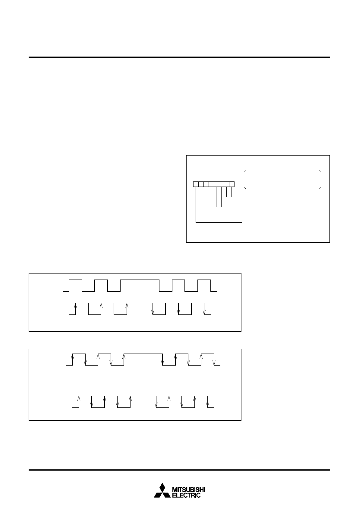
MITSUBISHI MICROCOMPUTERS
M37754M8C-XXXGP, M37754M8C-XXXHP
PRELIMINARY
Notice: This is not a final specification.
Some parametric limits are subject to change.
Data write and data read are performed in the same way as for timer
mode. That is, when data is written to timer Ai halted, it is also written
to the reload register and the counter. When data is written to timer
Ai which is busy, the data is written to the reload register, but not to
the counter. The counter is reloaded with new data from the reload
register at the next reload time. The counter can be read at any time.
Two-phase pulse processing
In event counter mode, whether to increment or decrement the
counter can also be determined by supplying two kinds of pulses of
which phases differ by 90° to timer A2, A3, or A4. There are two types
of two-phase pulse processing operations. One uses timers A2 and
A3, and the other uses timer A4. In both processing operations, two
pulses described above are input to the TA
TAj
IN pin respectively.
When timers A2 and A3 are used, as shown in Figure 25, the count is
incremented when a rising edge is input to the TAk
level of TAk
OUT(k=2,3) pin changes from “L” to “H”, and when the fall-
ing edge is input, the count is decremented.
For timer A4, as shown in Figure 26, when a phase-related pulse with
a rising edge input to the TA4
IN pin is input after the level of TA4OUT
pin changes from “L” to “H”, the count is incremented at the respective rising edge and falling edge of the T A4
When a phase-related pulse with a falling edge input to the TA4
pin is input after the level of TA4IN pin changes from “H” to “L”, the
count is decremented at the respective rising edge and falling edge
of the TA4
IN pin and TA4OUT pin. When performing this two-phase
pulse signal processing, timer Aj mode register bit 0 and bit 4 must
jOUT (j = 2 to 4) pin and
IN pin after the
OUT pin and TA4IN pin.
OUT
M37754S4CGP, M37754S4CHP
SINGLE-CHIP 16-BIT CMOS MICROCOMPUTER
be set to “1” and bits 1, 2, 3, and 5 must be “0”. Bits 6 and 7 are ignored. Note that bits 5, 6, and 7 of the up-down register (44
the two-phase pulse signal processing select bits for timers A2, A3
and A4 respectively. Each timer operates in normal event counter
mode when the corresponding bit is “0” and performs two-phase
pulse signal processing when it is “1”.
Count is started by setting the count start bit to “1”. Data write and
read are performed in the same way as for normal event counter
mode. Note that the direction register of the input port must be set to
input mode because two kinds of pulse signals, described above, are
input. Also, there can be no pulse output in this mode.
76543210
××
100010
Timer A2 mode register
Timer A3 mode register
Timer A4 mode register
0 1 : Always “01” in event counter mode
0 1 0 0 : Always “0100” when processing
two-phase pulse signal
× × : Not used in event counter mode
Fig. 27 Timer Aj mode register bit configuration when performing
two-phase pulse signal processing in event counter mode
Addresses
58
16
59
16
5A
16
16) are
TAkOUT
TAkIN
(k = 2, 3)
Increment-
count
Increment-
count
Increment-
count
Decrement-
count
Decrement-
count
Fig. 25 Two-phase pulse processing operation of timers A2 and timer A3
TA4OUT
Decrement-count at each edgeIncrement-count at each edge
TA4IN
Decrement-count at each edgeIncrement-count at each edge
Fig. 26 Two-phase pulse processing operation of timer A4
Decrement-
count
28
MITSUBISHI MICROCOMPUTERS
M37754M8C-XXXGP, M37754M8C-XXXHP
PRELIMINARY
Notice: This is not a final specification.
Some parametric limits are subject to change.
(3) One-shot pulse mode [10]
Figure 28 shows the bit configuration of the timer Ai mode register
during one-shot pulse mode. In one-shot pulse mode, bit 0 and bit 5
must be “0” and bit 1 and bit 2 must be “1”.
The trigger is enabled when the count start bit is “1”. The trigger can
be generated by software or it can be input from the TAi
ware trigger is selected when bit 4 is “0” and the input signal from the
TAi
IN pin is used as the trigger when it is “1“.
Bit 3 is used to determine whether to trigger at the fall of the trigger
signal or at the rise. The trigger is at the fall of the trigger signal when
bit 3 is “0” and at the rise of the trigger signal when it is “1”.
Software trigger is generated by setting the bit in the one-shot start
bit corresponding to each timer.
Figure 29 shows the bit configuration of the one-shot start register.
As shown in Figure 30, when a trigger signal is received, the counter
counts the clock selected by bits 6 and 7.
If the contents of the counter is not 0000
16, the TAiOUT pin goes “H”
when a trigger signal is received. The count direction is decrement.
When the counter reaches 0001
16, The TAiOUT pin goes “L” and
count is stopped. The contents of the reload register is transferred to
the counter. At the same time, an interrupt request signal is generated and the interrupt request bit in the timer Ai interrupt control register is set. This is repeated each time a trigger signal is received.
The output pulse width is
1
pulse frequency of the selected clock
× (counter’s value at the time of trigger).
If the count start flag is “0”, TAi
OUT goes “L”. Therefore, the value
corresponding to the desired pulse width must be written to timer Ai
before setting the timer Ai count start bit.
As shown in Figure 31, a trigger signal can be received before the
operation for the previous trigger signal is completed. In this case,
the contents of the reload register is transferred to the counter by the
trigger and then that value is decremented.
Except when retriggering while operating, the contents of the reload
register is not transferred to the counter by triggering.
When retriggering, there must be at least one timer count source
cycle before a new trigger can be issued.
Data write is performed in the same way as for timer mode.
When data is written in timer Ai halted, it is also written to the reload
register and the counter.
When data is written to timer Ai which is busy, the data is written to
the reload register, but not to the counter. The counter is reloaded
with new data from the reload register at the next reload time.
Undefined data is read when timer Ai is read.
IN pin. Soft-
M37754S4CGP, M37754S4CHP
SINGLE-CHIP 16-BIT CMOS MICROCOMPUTER
Timer A0 mode register
Timer A1 mode register
Timer A2 mode register
76543210
0110
Timer A3 mode register
Timer A4 mode register
1 0 : Always “10” in one-shot pulse mode
1 : Always “1” in one-shot pulse mode
0 × : Software trigger
1 0 : Trigger at the falling edge of TAi
input
1 1 : Trigger at the rising edge of TAi
input
0 : Always “0” in one-shot pulse mode
Clock source select
0 0 : Select Pf
0 1 : Select Pf
1 0 : Select Pf
1 1 : Select Pf
2
16
64
512
Fig. 28 Timer Ai mode register bit configuration during one-shot
pulse mode
76543210
One-shot start register
Timer A0 one-shot start bit
Timer A1 one-shot start bit
Timer A2 one-shot start bit
Timer A3 one-shot start bit
Timer A4 one-shot start bit
Fig. 29 One-shot start register bit configuration
Addresses
56
16
5716
58
16
59
16
5A
16
Address
42
16
IN
IN
29
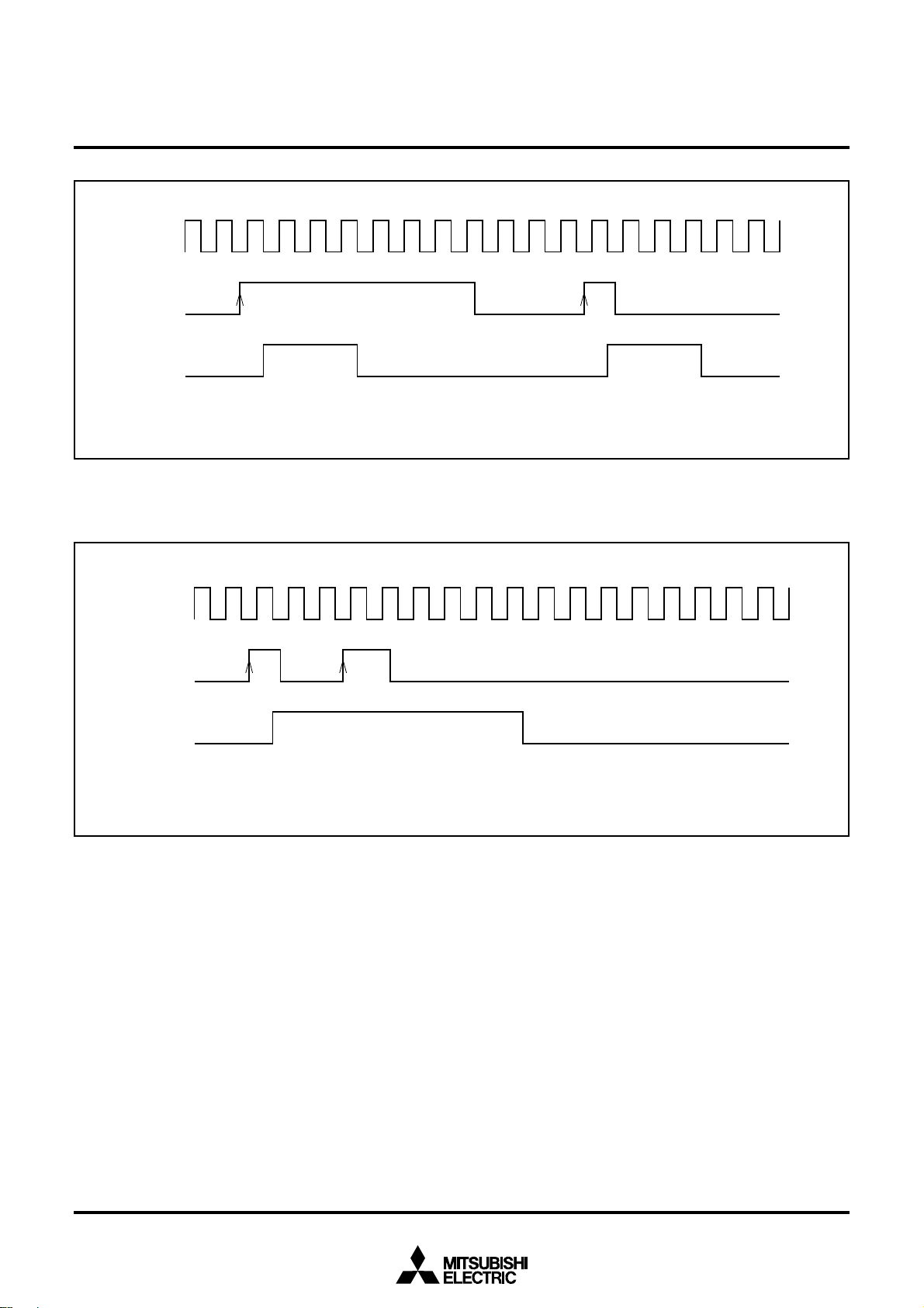
MITSUBISHI MICROCOMPUTERS
M37754M8C-XXXGP, M37754M8C-XXXHP
PRELIMINARY
Notice: This is not a final specification.
Some parametric limits are subject to change.
Selected clock
source Pfi
IN
TAi
(rising edge)
TAi
OUT
Example when the contents of the reload register is 000316
Fig. 30 Pulse output example when external rising edge is selected
M37754S4CGP, M37754S4CHP
SINGLE-CHIP 16-BIT CMOS MICROCOMPUTER
Selected clock
source Pfi
TAi
IN
(rising edge)
TAi
OUT
Example when the contents of the reload register is 000416
Fig. 31 Example when trigger is re-issued during pulse output
30
Loading...