

Page 1
SANYO Electric Co.,Ltd. Semiconductor Bussiness Headquaters
TOKYO OFFICE Tokyo Bldg., 1-10, 1 Chome, Ueno, Taito-ku, TOKYO, 110-8534 JAPAN
Any and all SANYO products described or contained herein do not have specifications that can handle
applications that require extremely high levels of reliability, such as life-support systems, aircraft’s
control systems, or other applications whose failure can be reasonably expected to result in serious
physical and/or material damage. Consult with your SANYO representative nearest you before using
any SANYO products described or contained herein in such applications.
SANYO assumes no responsibility for equipment failures that result from using products at values that
exceed, even momentarily, rated values (such as maximum ratings, operating condition ranges,or other
parameters) listed in products specifications of any and all SANYO products described or contained
herein.
Monolithic Digital IC
3-Phase Brushless Motor Driver
for CD-ROM Spindle Motors
Ordering number:EN4948A
LB1894M
Overview
The LB1894M is a 3-phase brushless motor driver for
use in CD-ROM spindle motors.
Function and Features
• 3-phase bipolar brushless motor driver.
• Voltage linear drive, enabling the external capacitance
to be reduced.
• Thermal shutdown circuit built-in.
• Overcurrent protection circuit built-in.
• V-type control amplifier built-in.
• 2-step switching control gain.
• Control gain switchable using operational amplifier.
Specifications
Absolute Maximum Ratings at Ta = 25˚C
retemaraPlobmySsnoitidnoCsgnitaRtinU
egatlovylppusmumixaM
tnerrucylppustuptuOV
tnerructuptuOI
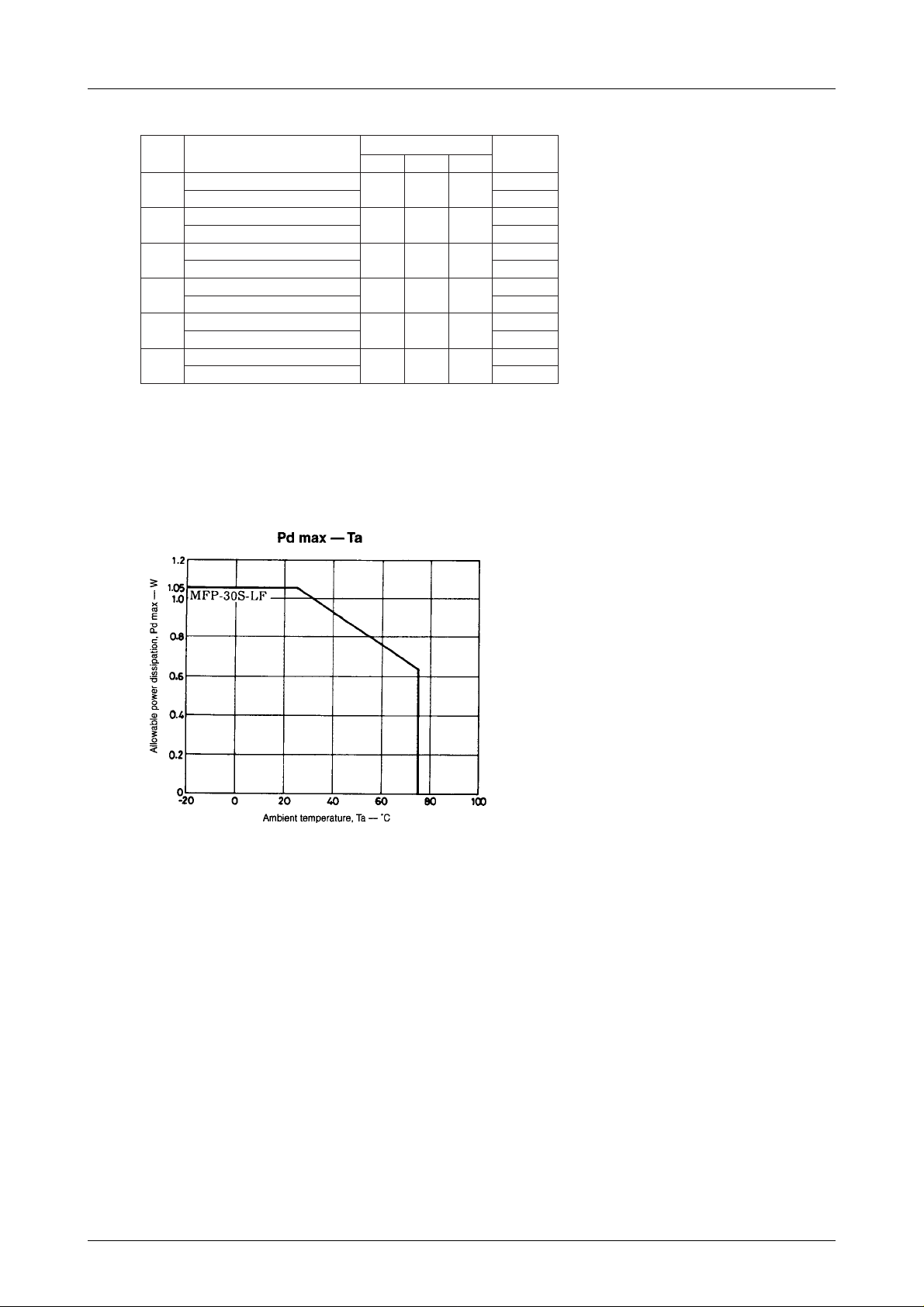
noitapissidrewopelbawollAxamdP 50.1W
erutarepmetgnitarepOrpoT 57+ot02–
erutarepmetegarotSgtsT 051+ot55–
V
V
xam1 02V
CC
xam2 0.7V
CC
W,V,UO
TUO
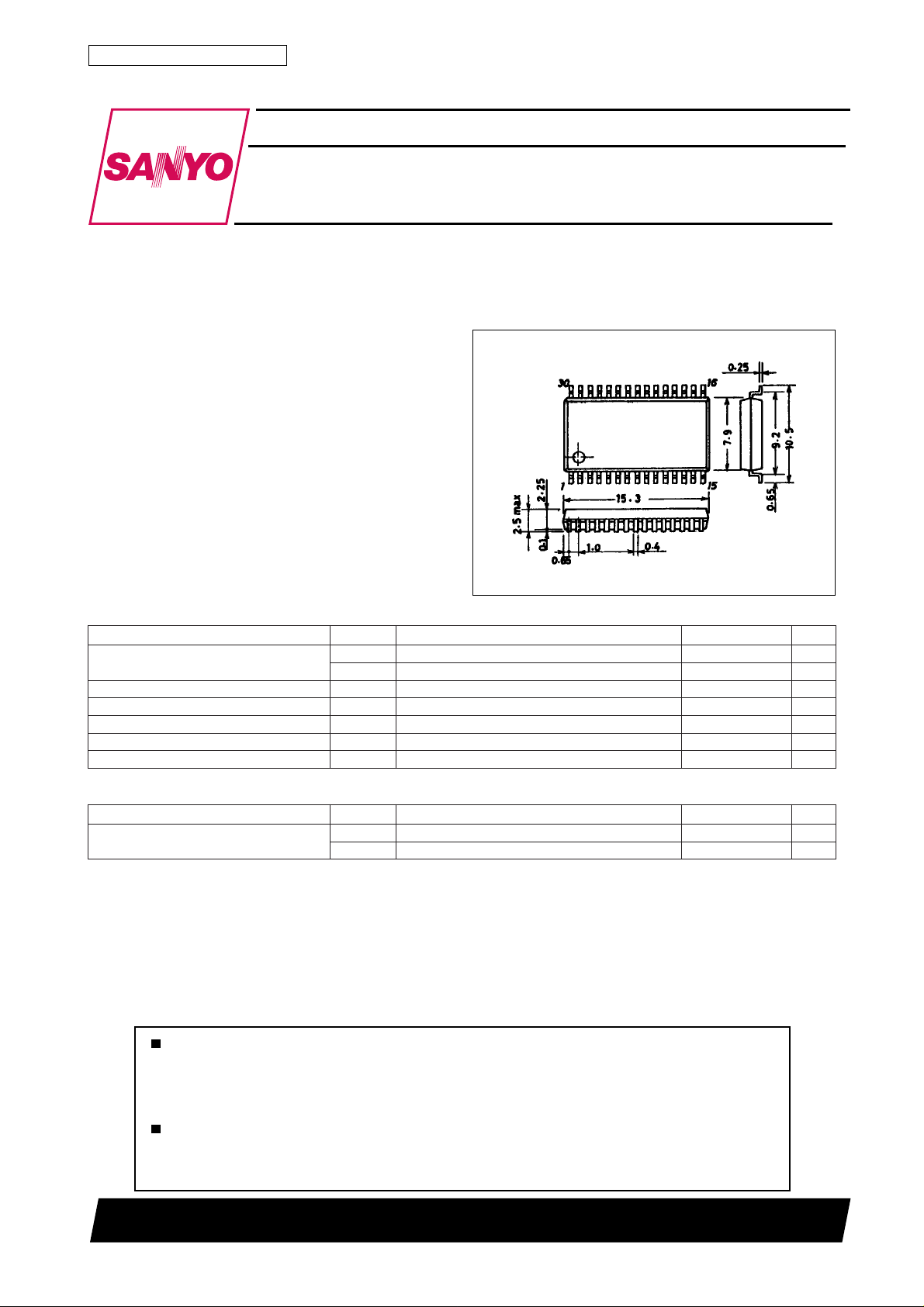
Package Dimensions
unit:mm
3073A-MFP30S
[LB1894M]
SANYO : MFP30S
22V
5.1A
˚C
˚C
Allowable Operating Ranges at Ta = 25˚C
retemaraPlobmySsnoitidnoCsgnitaRtinU
egatlovylppuS
VCC1 81ot5V
VCC2 5.6ot3.4V
93098HA (KT)/70695TH (ID) No.4948–1/7
Page 2
LB1894M
Electrical Characteristics at Ta = 25˚C, VCC1=12V, VCC2=5V
retemaraPlobmySsnoitidnoC
tnerrucylppuS
]egatsrevirD[
egatlovnoitarutastuptuO
egatlovgnikcolbrotsisnarttuptuOV
egatlovtsertuptuOV
egatlovtesffotupnireifilpmallaHV
tnerrucsaibtupnireifilpmallaHI
edom-nommocreifilpmallaH
egnaregatlovtupni
niagegatlovtuptuo-tupnireifilpmallaHG
]egatslortnoC[
niagevirdtuptuo-lortnoC
ecnereffidlennahctuptuo-lortnoC ∆G
egatlovdlohserhtgnisirlortnoCCV
htdiwegatlovdlohserhtgnisirlortnoC ∆ CV
egatlovlevel-hgihgnihctiwslortnocniaGV
egatlovlevel-wolgnihctiwslortnocniaGV
]sreifilpma-pO[
egatlovtesffotuptnireifilpma-pOV
niagegatlovpool-nepOG
egatlovnoitarutastuptuoecruoSV
egatlovnoitarutastuptuokniSV
noitcejerlangisedom-nommoCRHCeulavngiseD08Bd
nigramesahP φMeulavngiseD02ged
]nwodtuhslamrehT[
erutarepmetgnitareponwodtuhslamrehTDSTeulavngiseD051081012
siseretsyhDST ∆ DSTeulavngiseD51
ICC1CV=CV
ICC2CV=CV
V
1I
)tas(O
V
QO
V
hcH
OHV
G
OCV
G
OCV
HT
HCG
LCG
GFV
egnaregatlovtupniedom-nommocreifilpma-pOV
TUO
2I
)tas(O
TUO
I
)sus(O
TUO
CV=CV
tesffoH
saibH
1hgih=CG,niaghgiH235383Bd
2wol=CG,niagwoL629223Bd
OCV
CV
FER
CV
HT
UOGF
DOGF
HCGF
FER
tesffoGF
zHk1=f06Bd
I
O
IOAm2= 3.1V
CV
FER
=∞ 7103Am
FERR,L
FER
FER
V,V5.2=
TUO
V,V5.2=
TUO
Am2–=7.3V
VotV5.1=
CC
sgnitaR
nimpytxam
5.65.9Am
ecruos+knis,A5.0=6.12.2V
ecruos+knis,A0.1=0.20.3V
eulavngised,Am02=02V
7.50.63.6V
5–5+Vm
15Aµ
3.12.2V
245484Bd
2–2+Bd
p-pV1.0=53.256.2V
p-pV1.0=05051Vm
45V
nepotfelnehwlevelwolerastupnI02+V
8–8+Vm
eulavngised,205.3+V
tinU
˚C
˚C
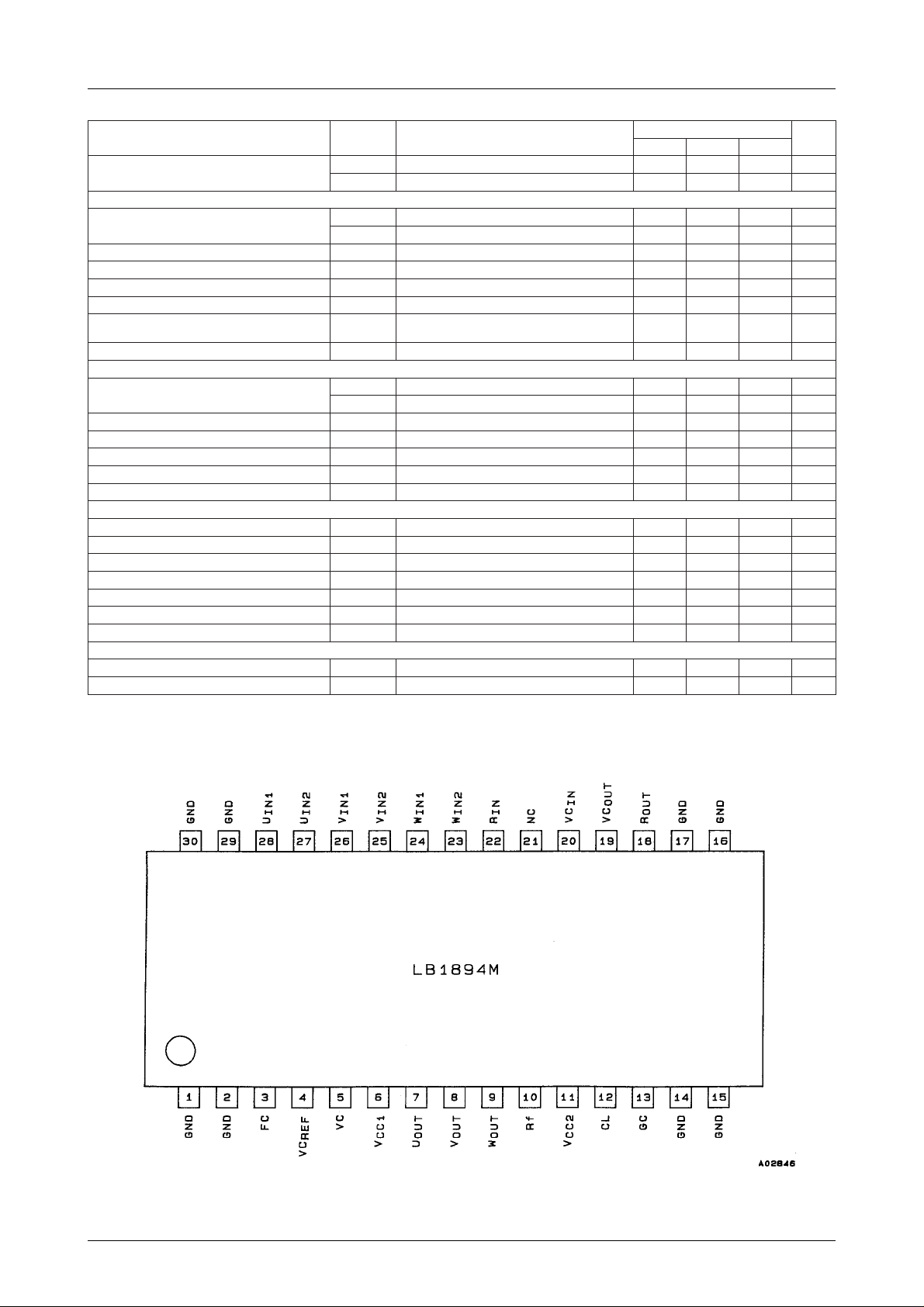
Pin Assignment
(Top view)
No.4948–2/7
Page 3
T ruth T able
LB1894M
ecruoS → kniS
1
2
3
4
5
6
esahp-W → esahp-V
esahp-V → esahp-WWOL
esahp-W → esahp-U
esahp-U → esahp-WWOL
esahp-V → esahp-W
esahp-W → esahp-VWOL
esahp-U → esahp-V
esahp-V → esahp-UWOL
esahp-V → esahp-U
esahp-U → esahp-VWOL
esahp-U → esahp-W
esahp-W → esahp-UWOL
U
NI
HGIHHGIHWOL
HGIHWOLWOL
WOLWOLHGIH
WOLHGIHWOL
HGIHWOLHGIH
WOLHGIHHGIH
tupnIllaH
V
W
NI
NI
lortnoC
CV
HGIH
HGIH
HGIH
HGIH
HGIH
HGIH
An input is considered to be HIGH when UIN1 > UIN2, VIN1 > VIN2, and WIN1 > WIN2 by 0.2V more, and is considered
to be LOW when UIN1 > UIN2, VIN1 > VIN2, and WIN1 > WIN2 by 0.2V or less.
No.4948–3/7
Page 4

Block Diagram 1
LB1894M
Block Diagram 2
No.4948–4/7
Page 5

Pin Functions
LB1894M
Pin No.
1, 2, 14,
15, 16,
17, 29,
30
3
4
5
Symbol Pin voltage Equivalent circuit Function
FRAME
(GND)
FC
VC
REF
VC
1.5V min
V
2 max
CC
0V min
2 max
V
CC
• Ground connection for all circuit except the outputs.
• Connect a capacitor between this pin and ground to
reduce the control input-output gain frequency
response and to stop the oscillator.
• Speed control pins.
Pin 4 voltage determines the control start voltage.
Pin 5 voltage is used to control the output voltage
(voltage control method).
6
V
1
CC
7
U
8
9
10
11
OUT
V
OUT
W
OUT
R
f
V
2
CC
5 to 18V
4.3 to 6.5V
• Output-stage supply pin.
• Output pins.
• Output transistor ground.
A resistor can be connected between this pin and
GND to sense the output current as a voltage drop to
provide for overcurrent protection.
• Supply for all circuits except the output stage.
This supply should be kept stable to prevent ripple
and noise from sntering this pin.
Continued to next page.
No.4948–5/7
Page 6

LB1894M
Pin No.
12
13
18
Symbol Pin voltage Equivalent circuit Function
• When the voltage on Rf pin becomes equal to the
voltage on pin 12 (CL), the current limiter operates.
The pin 12 (CL) voltage is determined externally.
If the current limiter is not used, it should be
CC
2
CL
0V min
2 max
V
CC
connected to V
• Control input gain switching pin.
35dB is selected when pin 13 (GC) is HIGH (4 to 5),
GC
0V min
2 max
V
CC
and 29dB is selected when pin 13 (GC) is LOW (0 to
2V) or open for a value V
CC
• A resistor connected between this pin and pin 20
) enables pin 22 switching between HIGH level
(VC
R
OUT
IN
and open to switch the op-amplifier gain.
2=5V.
• Op-amplifier output pin.
This op-amplifier can be used for :
19
VC
OUT
1. Control gain changing, or
2. FG amplifier.
• When this pin goes HIGH, the resistor connected
22
R
IN
between pins 18 and 20 is connected in parallel with
the op-amplifier feedback resistor to switch the gain.
• Op-amplifier inverting input pin.
20
VC
IN
0V min
3.5V max
(V
2=5V)
CC
The op-amplifier non-inverting input is connected to
pin 4 VC
REF
Continued to next page.
No.4948–6/7
Page 7

LB1894M
Pin No.
23
24
25
26
27
28
Symbol Pin voltage Equivalent circuit Function
W
2
IN
W
1
IN
V
2
IN
V
1
IN
U
2
IN
U
1
IN
1.3V min
2.2V max
• W-phase Hall element input pins.
Logic HIGH is represented by W
• V-phase Hall element input pins.
Logic HIGH is represented by V
• U-phase Hall element input pins.
Logic HIGH is represented by U
IN
IN
IN
1 > V
1 > W
1 > U
2.
IN
2.
IN
2.
IN
Specifications of any and all SANYO products described or contained herein stipulate the performance,
characteristics, and functions of the described products in the independent state, and are not guarantees
of the performance, characteristics, and functions of the described products as mounted in the customer’s
products or equipment. To verify symptoms and states that cannot be evaluated in an independent device,
the customer should always evaluate and test devices mounted in the customer’s products or equipment.
SANYO Electric Co., Ltd. strives to supply high-quality high-reliability products. However, any and all
semiconductor products fail with some probability. It is possible that these probabilistic failures could
give rise to accidents or events that could endanger human lives, that could give rise to smoke or fire,
or that could cause damage to other property. When designing equipment, adopt safety measures so
that these kinds of accidents or events cannot occur. Such measures include but are not limited to protective
circuits and error prevention circuits for safe design, redundant design, and structural design.
In the event that any and all SANYO products described or contained herein fall under strategic
products (including services) controlled under the Foreign Exchange and Foreign Trade Control Law of
Japan, such products must not be exported without obtaining export license from the Ministry of
International Trade and Industry in accordance with the above law.
No part of this publication may be reproduced or transmitted in any form or by any means, electronic or
mechanical, including photocopying and recording, or any information storage or retrieval system,
or otherwise, without the prior written permission of SANYO Electric Co. , Ltd.
Any and all information described or contained herein are subject to change without notice due to
product/technology improvement, etc. When designing equipment, refer to the “Delivery Specification”
for the SANYO product that you intend to use.
Information (including circuit diagrams and circuit parameters) herein is for example only ; it is not
guaranteed for volume production. SANYO believes information herein is accurate and reliable, but
no guarantees are made or implied regarding its use or any infringements of intellectual property rights
or other rights of third parties.
This catalog provides information as of September, 1998. Specifications and information herein are
subject to change without notice.
PS No.4948–7/7
 Loading...