

Page 1
SETUP SEQUENCE
Q 1
MIN MAX
ACTIVE ACTIVE
Q 3
MIN MAX
ACTIVE ACTIVE
Q 5
ACTIVE ACTIVE
Q 2
MIN MAX
Q 4
MIN MAX
Q 6
F 1F 2F 3F 4F 5F 6
F 1 F 2 F 3 F 4 F 5 F 6
PAD BANK
BC
A
A
BCDEFGH
Q-LINK
SEQUENCE
&
PAD
ASSIGN
#
FULL
LEVEL
16
LEVELS
!
ERASE
(
NOTE
REPEAT
)
PAD 13 PA D 14 PAD 15 PAD 16
PAD 9 PAD 10 PAD 11 PAD 12
PAD 5 PAD 6 PAD 7 PAD 8
PAD 1 PAD 2 PAD 3 PAD 4
D
P LOOP PTO P FROM
DRUMS
F
E
NEXT
SEQUENCE
CONTRAST
REC GAIN
MAIN VOLUME
GAIN
HIGH
LOW
MAX
MINMIN MAX
R
L
SAMPLE
MULTI
SAVE LOAD
SONG MISC.
MAIN
SEQ EDIT
JOG
START END
PROGRAM
MIXER
EFFECT
GLOBAL
MIDI
STEP EDIT
BLOCK
CURSOR
BAR
PLAY
PLAY
START
RECORD
STEP
EVENT
OVER
DUB
IJK
LMN
OPQ
RST
UVW
CURSOR
LOCATE
GO TO
PLAY/ REC
STOP
TRACK
MUTE
PLAY
789
456
123
TIMING CORRECT
X
MASTER TEMPO
Y
UNDO SEQ
Z
TAP TEMPO
0 ENTER
WINDOW
SHIFT
REC
Music production Center
SERVICE MANUAL
1
Page 2
##
# SAFETY INSTRUCTIONS
##
##
# INFORMATIONS
##
1. Parts identified by the } symbol are critical for safety.
Replace them only with the parts number specified.
2. In addition to safety, other parts and assemblies are
specified for conformance with such regulations as those
applying to spurious radiation.
These must also be replaced only with the specified
replacements.
Examples : Noise blocking capacitors, noise blocking filters,
etc.
3. Use specified internal wiring. Note especially :
1) Wires covered with PVC tubing
2) Double insulated wires
3) High voltage leads
4. Use specified insulating materials for hazardous live parts.
Note especially :
1) Insulation Tape
2) PVC tubing
3) Spacers (insulating barriers)
4) Insulation sheets for transistors
5) Plastic screws for fixing micro switches
5. When replacing AC primary side components (transformers, power cords, noise blocking capacitors, etc.),
wrap the ends of the wires securely around the terminals
before soldering.
SYMBOLS FOR PRIMARY DESTINATION
Unit destinations are indicated with letters as shown below.
Symbols Principal Destinations
A U.S.A
B England
E Europe
J Japan
V
X1
X4
MAKE YOUR CONTRIBUTION TO PROTECT THE
ENVIRONMENT
Used batteries with the ISO symbol for recycling as
well as small accumulators (rechargeable batteries),
mini-batteries (cells) and starter batteries should not
be thrown into the garbage can.
Please leave them at an appropriate depot.
PRECAUTIONS FOR LITHIUM BATTERY
The lithium battery may explode when
[OBSERVE THE FOLLOEING WHEN REPLACING]
Germany
Japan
Universal Area
incorrectly replaced.
6. Make sure that wires do not contact heat producing parts
(heat sinks, oxide metal film resistors, fusible resistors,
etc.).
7. Check that replaced wires do not contact sharp edged or
pointed parts.
8. Also check areas surrounding repaired locations.
9. Make sure that foreign objects (screws, solder droplets,
etc.) do not remain inside the set.
SAFETY CHECK AFTER SERVICING
After servicing, make measurements of leakage-current or
resistance in order to determine that exposed parts are
acceptably insulated from the supply circuit. The leakagecurrent measurement should be done between accessible
metal parts (such as chassis, ground terminal, microphone
jacks, signal input/output connectors, etc.) and the earth ground
through a resistor of 1500 ohms paralleled with a 0.15 µF
capacitor, under the unit’s normal working conditions.
The leakage-current should be less than 0.5 mA rms AC. The
resistance measurement should be done between accessible
exposed metal parts and power cord plug prongs with the
power switch (if included) “ON”. The resistance should be
more than 2.2 M ohms.
• Replace with the same make and type or equivalent recom
mended by manufacturer.
• Place battery in correct polarity.
• Do not short the terminals.
• Do not charge battery.
• Do not dispose of battery in fire.
SERVICE MANUAL
2
Page 3

I. SPECIFICATIONS
General Power supply 100-240V AC 50/60Hz 70W (27W without options)
Dimensions 526 (W) x 170 (H) x 453 (D) mm (with LCD tilted down)
Weight 10.5kg (without options)
Display 320 x 240 dots grey-scale graphical LCD w/back light
Sound Generator Sampling rate 44.1kHz, 48kHz, 96kHz
Data format 24/16 bit linear
Sampling time 180/120 (16/24 bit) seconds mono FS=44.1kHz
(unexpanded memory) 166/110 (16/24 bit) seconds mono FS=48kHz
82/53 (16/24 bit) seconds mono FS=96kHz
90/60 (16/24 bit) seconds stereo FS=44.1kHz
83/55 (16/24 bit) seconds stereo FS=48kHz
40/26 (16/24 bit) seconds stereo FS=96kHz
Memory 16MB standard, expandable to 512MB
168-pin DIMM (PC133/PC100, CL2) slot x 2
Polyphony 64 voices
Filter 2-pole x 3 with resonance
Envelope generators 3 x Envelope generators (2 multi-stage)
LFO 2 x Multi-wave
Sequencer Maximum events 300,000 notes (equivalent)
Resolution 960 parts per 1/4-note (ppq)
Sequences 128
Tracks per sequence 128
MIDI output channels 64 (16 channels x 4 output ports)
Song mode 128 songs, 250 steps per song
Drum pads 16 (velocity and pressure sensitive)
Drum pads banks 6
Sync modes MTC, MIDI clock, SMPTE
Inputs/Outputs Rec In LINE/MIC L/R 1/4-inch stereo phone/XLR Combo jack, balanced,
1/4-inch phone, Imp. 18kΩ, 24dBu max./XLR, Imp. 6kΩ, 22dBu max.
Rec In PHONO L/R RCA phono x 2 with RIAA EQ, -24dBu max. (1kHz)
Main Out L/R 1/4-inch stereo phone/XLR Combo jack, balanced,
1/4-inch phone, Imp. 1.7kΩ, 24dBu max./XLR, Imp. 200Ω, 18dBu max.
Assignable Outs (IB-48P
required) 1/4-inch stereo phone x 8, balanced, Imp. 1.7kΩ, 18dBu max.
Headphone 1/4-inch stereo phone, 60mW (32Ω)
Digital Input (IB-4D required) RCA phono x 1, SPDIF
Digital Main Output
(IB-4D required) RCA phono x 1, SPDIF
Word Clock Input
(IB-4D required) BNC x 1 (w/75Ω terminator On/Off)
SMPTE In 1/4-inch stereo phone, balanced
SMPTE Out 1/4-inch stereo phone, balanced
Footswitch 1/4-inch phone x 2
MIDI Input 5-pin DIN x 2
MIDI Output 5-pin DIN x 4
SCSI 50-pin high-pitch SCSI connector x 1
USB Host x 1, Slave x 1 (V1.1)
Options IB-4D Digital Audio (SPDIF) I/O board
IB-4ADT Adat Interface board (2-in/8-out)
IB-48P Assignable 8-channel Output Board
Standard accessory Power Cable x 1
CD-ROM disc x 1
Drive Mounting Kit x 1
User Guide x 1
* The specifications are subject to change without the prior notice.
SERVICE MANUAL
3
Page 4
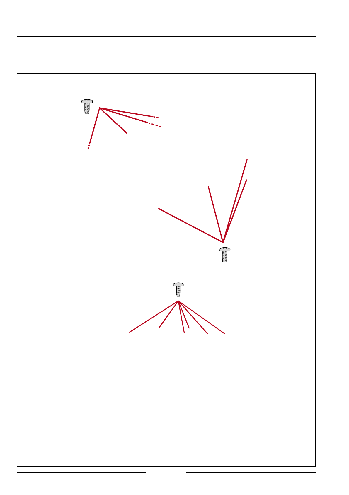
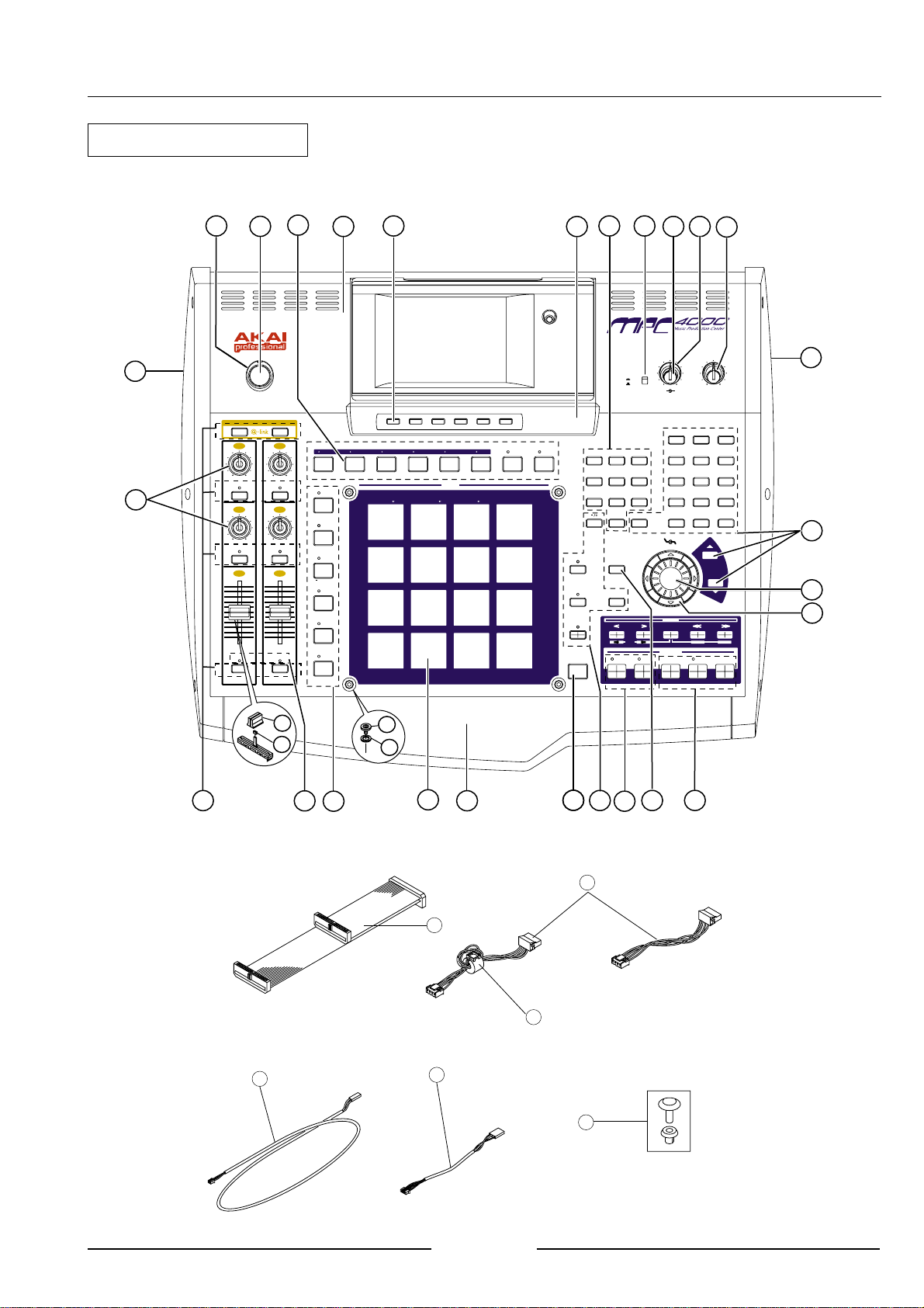
II. DISASSEMBLY
In case of trouble, etc., necessitating dismantling, please dismantle in the order shown in the illustrations. Reassemble in the
reverse order.
1. Removal of the OPERATION BLOCK
ZS-322570
ST BID40X08STL NI3
ZS-331182
BT BID30X08STL BNI
SERVICE MANUAL
4
Page 5
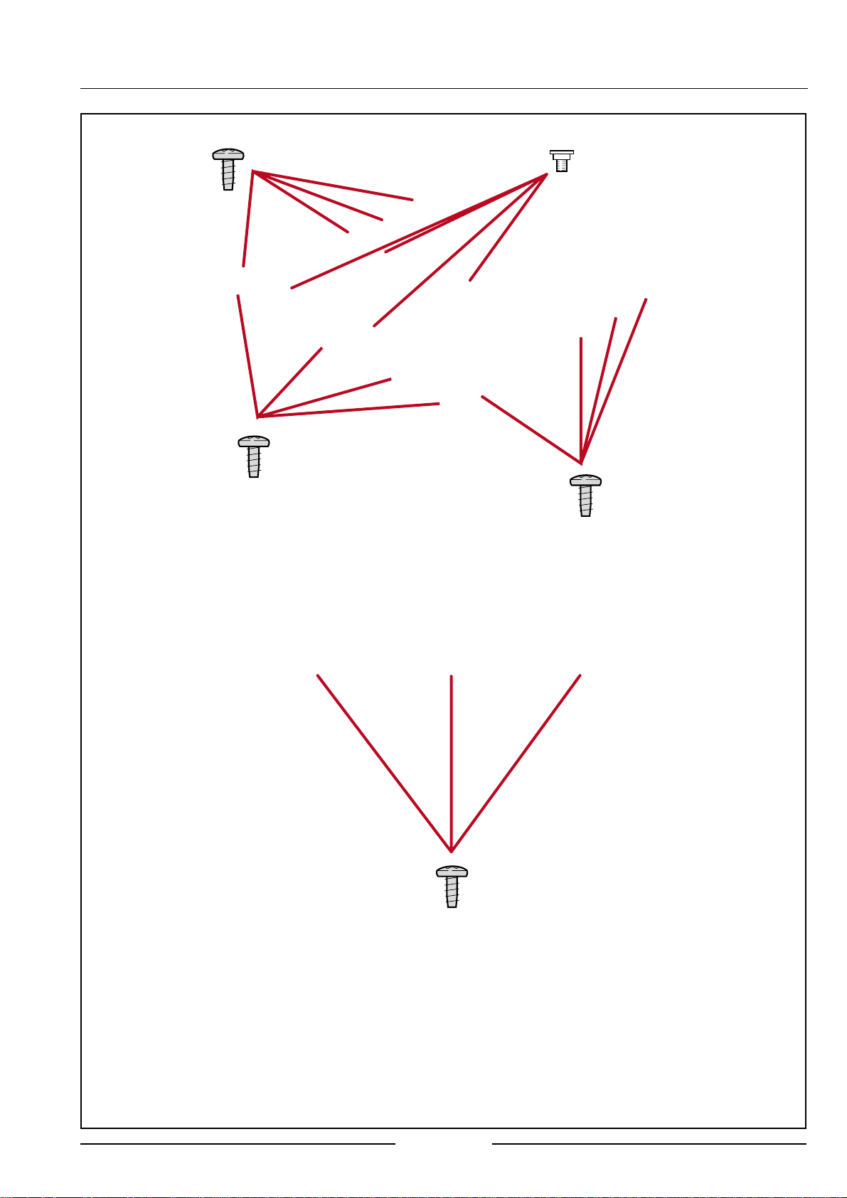
ZS-331182
BT BID30X08 STL BNI
ZS-821548X SCREW TOP COVER NI
ZS-331182
BT BID30X08 STL BNI
SERVICE MANUAL
5
Page 6
ZS-331182
BT BID30X08 STL BNI
SERVICE MANUAL
6
Page 7

III. PRINCIPAL PARTS LOCATION
EM-812761J
IND LCD
BA-L4016A504F
PC POWER SW BLK
BA-L4016A504C
PC LCD BLK
BA-L4016A502C
PC IO VR BLK
BA-L4016A504B
PC FUNCTION BLK
BA-L4016A504A
PC JOG BLK
BA-L4016A030A
PC OPERATION BLK
BA-L4016A504E
PC FILTER BLK
BA-L4016A502A
PC IO BLK
BA-L4016A502B
PC IO ADDA BLK
BA-L6052A020A
PC CPU BLK Z8
BA-LJ038A020A
PC POWER BLK SPS-80
BA-L4016A504D
PC HEAD PHONE & USB BLK
SERVICE MANUAL
EB4JS
7
Page 8

IV. OS Update Procedure
OS Update Procedure
[OS Update procedure from USB]
The OS update can be made from the PC via the USB port.
You must have the “OS loader software for MPC4000” besides the OS .bin file.
The OS loader software includes the OS Loader.exe file, USB driver.inf file, and USB Driver.sys file.
1. Install USB Driver to your PC
After all files are un-Zipped, place the USB Driver.inf and USB Driver.sys files into the same folder, e.g. Driver.
Boot up the PC and MPC4000 complete and then connect the sampler to the PC using the USB cable.
This prompts that the PC found the new device an d the new driver is required.
Refer it to the Driver folder you just created.
The Driver software will be placed correctly and the MPC4000 is recognized properly.
2. OS update
Double click on the OS Loader.exe icon and specify the OS .bin file. It will send the OS to the MPC4000.
[Caution]
After the update, be sure to initialize the MPC4000 by pressing the GLOBAL key, and then [F6] (INITIAL)
and [F5] (DO IT) keys, before turning it off.
[OS update procedure from CD-R]
To update the OS from the CD-ROM, it requires the OS version later than V1.02 software installed on the MPC4000.
You can update the OS from the CD-ROM drive. Be sure to use the CD-ROM that contains the OS for the MPC
4000. You can create the OS disc by using your PC’s CD-R/W function to write the “MPC4000.bin” file on to an
ISO9660 CD-ROM disc.
1. Turn the MPC4000 on and insert the OS disc.
2. Press the LOAD key and select the MPC4000 OS file (.bin file).
3. Press the [F6] (DO IT) key and then the [F6] (INSTALL) key.
4. The OS Update progress appears, i.e. the messages “Please wait ??.” and then “Upgrading of the Flash
ROM was successful.” appear accordingly.
5. Press the [F6] (Restart) key. Be sure to initialize the MPC4000 by pressing the GLOBAL key, and then the
[F6] (INITIAL) and [F5] (DO IT) keys, before turning it off.
Writing Panel OS Program
Change the position of the Short Pin P15 on the IO PCB to PROG side.
The OS is automatically written to the Panel CPU RAM when the MPC4000 is switched on.
Switch the unit off when the “Process completed!” prompt message appeared and then replace the Short Pin to the
original position.
SERVICE MANUAL
8
Page 9

V. TEST MODE
Panel Test Mode
To enter the Panel Test Mode, press the GLOBAL key while holding down the SHIFT key in the GLOBAL page [F1] of the
GLOBAL Mode.
• Moving the Q-link knobs changes the graphics accordingly.
• Tapping the PAD shows the amount of pressure applied on the bar graph.
• Switching the FOOT Pedal on/off changes the graphics accordingly.
• Turning the JOG wheel increases/decreases the value in the Data field.
• Pressing the key shows its name at the bottom of the screen. For those keys with the LED, the LED is turned
on/off.
• Pressing the [F1] key stops the key test.
• After stopping the key test, pressing the mode key will abort the test mode.
• While the key test is stopped, pressing the SHIFT key and [F6] key shows the A/D converted value of the
Q-link/ PAD.
CPU Board Test Mode
The Test Mode of the MPC4000 CPU Board is performed while the CPU board is mounted on the Z4/Z8 Sampler.
When the Z4/Z8 is switched on after the MPC4000 CPU Board is mounted on the Z4/Z8 Sampler, the sampler
is turned on with the MPC4000 screen.
Install the Z4/Z8 OS using the “OS Loader” of “Boot Overwrite” type via the USB port.
Similarly, when the CPU Board is mounted back on the MPC4000 after the Z4/Z8 OS is installed for the test,
it boots up with the Z4/Z8 screen. Reinstall the MPC4000 OS using the “OS Loader” of “Boot Overwrite” type.
Refer to the Z4/Z8 Service Manual for the operation details of the Test Mode for the CPU Board.
SERVICE MANUAL
9
Page 10

VI. PARTS LIST
ATTENTION
1. When placing an order for parts, be sure to list the Part No., Model No. and the description of each part.
Otherwise, the non-delivery of the part or the delivery of a wrong part may result.
2. Please make sure that Part No. is correct when ordering.
If not, a part different from the one you ordered may be delivered.
3. Since the parts shown in Parts List or Preliminary Service Manual may have been the subject of changes,
please use this Parts List for all future reference.
HOW TO USE THIS PARTS LIST
1. This Parts List lists those parts which are considered necessary for repairs.
2. Parts not shown in the Parts List will not in principle be supplied.
3. How to read the Parts List.
1. PC MAIN BOARD BLK
Ref. No. Part No. Description
D5 ED-431276C D SCHOT 1S30-J T05
D110 ED-431276C D SCHOT 1S30-J T05
:
:
IC5 EI-811073J ICTRC-6593
IC10 EI-811068J IC HD74HC157FP
Service parts classification
These reference symbols correspond with component
symbols in the Schematic Diagrams.
2. FINAL ASSEMBLY BLK
Ref. No. Part No. Description
1. SA-349332 FOOT
2. ZS-344754C ST PAN30x06STL CMT
:
:
44. SP-417333J COVER TOP
45. ZS-418385J BT BID30X06STL BNI EATRH LOCK
46-A } EW-380905J AC CORD 250S KP300 KS16A
H B J [J]
46-B } EW-368420J1 AC CORD 200SKP30KS B AC [A]
46-C } EW-410608J AC CORD 250 KP4819D KS31A B E
[E,V]
Symbols for primary destination
[A] U.S.A. [J] Japan
[B] England [V] Germany
[E] Europe [x1] Japan
[X4] Universal Area
Safety critical component
This number corresponds with the individual parts index number
in the figure.
WARNING
}}
} INDICATES SAFETY CRITICAL COMPONENTS. FOR CONTINUED SAFETY, REPLACE SAFETY CRITICAL
}}
COMPONENTS ONLY WITH MANUFACTURER'S RECOMMENDED PARTS.
AVERTISSEMENT
}}
} IL INDIQUE LES COMPOSANTS CRITIQUES DE SÉCURITÉ. POUR MAINTENIR LE DEGRÉ DE SÉCURITÉDE
}}
L'APPAREIL, NE REMPLACER QUE DES PIÉCES RECOMMANDEES PAR LÉ FABRICANT.
SERVICE MANUAL
10
Page 11

PC BOARD BLK
The PC Board Block may contain several PC Boards. They appear
under its block name with their individual part number.
1. P.C. BOARD BLOCK
Ref.No. Part No. Description
1 BA-L6052A020A PC CPU BLK Z8
2 BA-L4016A020A PC (#) IO BLK MPC4000
3 BA-L4016A030A PC OPERATION BLK MPC4000
4 BA-L4016A040A PC (#) OTHER BLK MPC4000
PC (#) IO BLK CONSISTS OF FOLLOWING P.C. BOARDS.
✽ BA-L4016A502A PC IO BLK
✽ BA-L4016A502B PC IO ADDA BLK
✽ BA-L4016A502C PC IO VR BLK
PC (#) OTHER BLK CONSISTS OF FOLLOWING P.C. BOARDS.
✽ BA-L4016A504A PC JOG BLK
✽ BA-L4016A504B PC FUNCTION KEYS BLK
✽ BA-L4016A504C PC LCD BLK
✽ BA-L4016A504D PC HEAD PHONE & USB BLK
✽ BA-L4016A504E PC FILTER BLK
✽ BA-L4016A504F PC POWER SW BLK
2. P.C. CPU BLOCK
Ref.No. Part No. Description
IC1 EI-820788X IC GDS1110BD-206MHZ MBGA
[ unavailable ]
IC2 EI-821551X IC MB87L1852PFVS-G-BND JSL
IC3 EI-821594X IC HM5264165FTT-75
IC4 EI-821594X IC HM5264165FTT-75
IC5 EI-821424X IC HY57V281620AT-7 FPTY
IC6 EI-821424X IC HY57V281620AT-7 FPTY
IC7 EI-821211X IC MBM29DL322TE90TN
IC8 EI-820962X IC XC95144XL-7TQ100C
IC9 EI-820961X IC XC2S100-5TQ144C
IC10 EI-820959X1 IC SL811HST V1.5
IC11 EI-812785J IC FAS236U PQFP
IC12 EI-820949X IC HD74ALVCH16245TEL
IC13 EI-820948X IC HD74ALVCH16244TE
IC14 EI-820948X IC HD74ALVCH16244TE
IC15 EI-820948X IC HD74ALVCH16244TE
IC16 EI-820949X IC HD74ALVCH16245TEL
IC17 EI-820951X IC HD74LVC244AT FPELT16E
IC18 EI-820951X IC HD74LVC244AT FPELT16E
IC19 EI-812979J IC HD74LVC245ATELL FPELT16E
IC20 EI-810574J IC M51957BFP FP73AT12
IC21 EI-820957X IC NJM317DL1 FPTE1T16E
IC22 EI-820957X IC NJM317DL1 FPTE1T16E
IC23 EI-820955X IC NET2890
J1 EJ-820938X SOCKET SMD XH4A-8035-A 80P
J2 EJ-820938X SOCKET SMD XH4A-8035-A 80P
J3 EJ-820937X SOCKET SMD XH4A-4035-A 40P
J4 EJ-820937X SOCKET SMD XH4A-4035-A 40P
J5 EJ-820990X SOCKET DMM-168F-111B1 168P
J6 EJ-820990X SOCKET DMM-168F-111B1 168P
J7 EJ-419246J SOCKET 128A-050S2A-S14A 50P
P2 EJ-810581J PLUG SCP40GS3 40P
P2 EJ-810581J PLUG SCP40GS3 40P
P4 EJ-432670J PLUG C.S6B-PH-SM3-TB 6P T24E
P5 EJ-821159X PLUG C.S5B-PH-SM3-TB 5P T24E
P6 EJ-820998X PLUG C.S4B-PH-SM3-TB 4P T24E
TR1 ET-430868J TR C.DTC114EKA T146T08E
TR2 ET-430868J TR C.DTC114EKA T146T08E
TR3 ET-430868J TR C.DTC114EKA T146T08E
UN1 EI-820944X DC-DC CONVERTER HGS15-3R3
Ref.No. Part No. Description
X1 EI-820769X OSC X'TAL C.SMD-49 3.6864MHZ
X2 EI-820994X OSC X'TAL C.DS0751SV 18.4320MHZ
X3 EI-820993X OSC X'TAL C.DS0751SV 16.9344MHZ
X4 EI-820991X OSC X'TAL C.SMD-49 12.0000MHZ
X5 EI-820995X OSC X'TAL C.DS0751SB 40.0000MHZ
X6 EI-820989X OSC X'TAL C.DS0751SV 48.0000MHZ
3. P.C. IO BLOCK
Ref.No. Part No. Description
100 EZ-811066J BATTERY LITHIUM CR2025
400 ES-429984J SOCKET IC113-0444-004 44P
D1 ED-811455J D SILICON H 1SS133T-77 T26
D2 ED-811455J D SILICON H 1SS133T-77 T26
D3 ED-428162J D SCHOTTKY 1S30-E T26
D4 ED-428162J D SCHOTTKY 1S30-E T26
D5 ED-820774X D SCHOT.H EK16 V0 T26 60/1.5A
D6 ED-811455J D SILICON H 1SS133T-77 T26
D7 ED-811455J D SILICON H 1SS133T-77 T26
D8 ED-811455J D SILICON H 1SS133T-77 T26
D9 ED-811455J D SILICON H 1SS133T-77 T26
D30 ED-811455J D SILICON H 1SS133T-77 T26
D31 ED-811455J D SILICON H 1SS133T-77 T26
D32 ED-811455J D SILICON H 1SS133T-77 T26
D33 ED-811455J D SILICON H 1SS133T-77 T26
FS1
IC1 EI-821048X IC UPC29M33AT-E2 FPE2T16E
IC2 EI-811073J IC RTC-6593
IC3 EI-396659J IC NJM2360D
IC4 EI-820062J IC HD74HCT541FP FPELT24
IC5 EI-821116X IC HD74HCT04AFP FPELT16E
IC6 EI-810828J IC MCCS142236DWR2 18B
IC7 EI-812979J IC HD74LVC245ATELL FPELT16E
IC8 EI-812979J IC HD74LVC245ATELL FPELT16E
IC9 EI-812977J IC HD74LVC08TELL FPELT16E
IC10 EI-431113J IC M51953BFP-73A FP73AT12E
IC11 EI-821593X IC ICS2008BV
IC12 EI-380145J IC LF353
IC13 EI-821344X IC TC74HCT32AF-EL FPELT16
IC14 EI-812980J IC HD74LVC32TELL FPELT16E
IC15 EI-812979J IC HD74LVC245ATELL FPELT16E
IC16 EI-812980J IC HD74LVC32TELL FPELT16E
IP1 EF-373285 FUSE ICP-N25 T05 50V 1.0A
J1 EJ-430956J DIN J YKF51-5058 2X5P
J2 EJ-430956J DIN J YKF51-5058 2X5P
J3 EJ-430956J DIN J YKF51-5058 2X5P
J5 EJ-820493X SOCKET BATTERY BH25TN
J6 EJ-820316X SOCKET CONNECTER YKF45-
J8 EJ-820939X SOCKET XH4A-8031-A 80P
J9 EJ-820939X SOCKET XH4A-8031-A 80P
J10 EJ-821219X PHONE J YKB22-5244 NUT 6.3
J11 EJ-821219X PHONE J YKB22-5244 NUT 6.3
J12 EJ-812347J SOCKET FCN-235D050-G/J 50P
J13 EJ-821386X PHONE J YKB22-5264 NUT 6.3
J14 EJ-821386X PHONE J YKB22-5264 NUT 6.3
L1 EO-812743J COIL FIX 1 LHL10NB 821K
P14 EJ-810270J PLUG SCP50GS3 50P
P2 EJ-810271J PLUG SCP26GS3 26P
P3 EJ-810581J PLUG SCP40GS3 40P
P3 EJ-810581J PLUG SCP40GS3 40P
P4 EJ-810270J PLUG SCP50GS3 50P
P9 EJ-810271J PLUG SCP26GS3 26P
PH1 EJ-431258J DETECTOR C.PC400T T12E
PH2 EJ-431258J DETECTOR C.PC400T T12E
EF-811786J FUSE RUE110 30V 1.10A
FPR2T24E
0001 4P
SERVICE MANUAL
11
Page 12

Ref.No. Part No. Description
R23
R77
TR1 ET-429896J TR C.DTA144EKA T146T08E
TR2 ET-429897J TR C.DTC144EKA T146T08E
TR3 ET-434246J TR 2SB1326 Q,R T05
TR4 ET-362209 TR 2SC3330 S,T,U T05
TR5 ET-430868J TR C.DTC114EKA T146T08E
TR6 ET-429898J TR C.DTA114EKA T146T08E
P.C. IO ADD BLOCK
X1 EI-410263J OSC X'TAL HC-49/U 14.318180MHZ
D10 ED-811455J D SILICON H 1SS133T-77 T26
D11 ED-811455J D SILICON H 1SS133T-77 T26
D12 ED-811455J D SILICON H 1SS133T-77 T26
D13 ED-811455J D SILICON H 1SS133T-77 T26
D14 ED-811455J D SILICON H 1SS133T-77 T26
D15 ED-811455J D SILICON H 1SS133T-77 T26
D16 ED-811455J D SILICON H 1SS133T-77 T26
D17 ED-811455J D SILICON H 1SS133T-77 T26
D18 ED-811455J D SILICON H 1SS133T-77 T26
D19 ED-811455J D SILICON H 1SS133T-77 T26
D20 ED-811455J D SILICON H 1SS133T-77 T26
D21 ED-811455J D SILICON H 1SS133T-77 T26
D22 ED-811455J D SILICON H 1SS133T-77 T26
D23 ED-811455J D SILICON H 1SS133T-77 T26
D24 ED-811455J D SILICON H 1SS133T-77 T26
IC21 EI-348785 IC M5220L
IC22 EI-348785 IC M5220L
IC23 EI-348785 IC M5220L
IC24 EI-397407J IC NJM7812FA
IC25 EI-348785 IC M5220L
IC26 EI-348785 IC M5220L
IC27 EI-810591J IC NJM5532L
IC28 EI-348785 IC M5220L
IC29 EI-810591J IC NJM5532L
IC30 EI-812781J IC AK5383VS FPE2T24E
IC31 EI-820696X IC ICS570A-01CS08 FP T12E
IC32 EI-821120X IC HD74LVC02TELL FPELT12E
IC33 EI-810574J IC M51957BFP FP73AT12
IC34 EI-336995 IC NJM78L05A
IC35 EI-810574J IC M51957BFP FP73AT12
IC36 EI-821442X IC PCM1730E FPT16E
IC37 EI-821226X IC OPA2134UA FPT12E
IC38 EI-821226X IC OPA2134UA FPT12E
IC39 EI-810591J IC NJM5532L
IC40 EI-377191 IC NJM5532D-D
IC41 EI-377191 IC NJM5532D-D
IC42 EI-377191 IC NJM5532D-D
IC43 EI-377191 IC NJM5532D-D
IC44 EI-348785 IC M5220L
IC45 EI-410281J IC NJM7912FA
IC46 EI-821118X IC NJM78M08FA
IC47 EI-400856J IC NJM78M05FA
IC48 EI-400856J IC NJM78M05FA
IC49 EI-821118X IC NJM78M08FA
IC50 EI-821048X IC UPC29M33AT-E2 FPE2T16E
IC51 EI-812977J IC HD74LVC08TELL FPELT16E
IC52 EI-820951X IC HD74LVC244AT FPELT16E
IC53 EI-810588J IC SSM-2404P
J21 EJ-820762X SOCKET RECEPTACLE NCJ9FI-H-0
J22 EJ-820762X SOCKET RECEPTACLE NCJ9FI-H-0
J23 EJ-821443X PIN J YKC21-3079 P2P
J24 EJ-386340J SOCKET RECEPTACLE XLB3-
J25 EJ-386340J SOCKET RECEPTACLE XLB3-
J26 EJ-821386X PHONE J YKB22-5264 NUT 6.3
ER-812771J R OMF V T05FS ERX12SE1/2W 1R0J
ER-821483X R OMF H S15 FS ERG2SH 2W 820J
32PCVM1
32PCVM1
Ref.No. Part No. Description
J27 EJ-821386X PHONE J YKB22-5264 NUT 6.3
R361 ER-422512J R OMF H S15 FS ERG2SH 2W 151J
RL1 EQ-348929 RELAY SIG G5A-237P 2TR 12V
RL2 EQ-348929 RELAY SIG G5A-237P 2TR 12V
SW1 ES-821121X SW SLIDE SSSF142-S09N0 4-02N
TR10 ET-821232X TR 2SC3329 GR,BL T05
TR11 ET-821232X TR 2SC3329 GR,BL T05
TR12 ET-821232X TR 2SC3329 GR,BL T05
TR13 ET-821232X TR 2SC3329 GR,BL T05
TR14 ET-821232X TR 2SC3329 GR,BL T05
TR15 ET-821232X TR 2SC3329 GR,BL T05
TR16 ET-821232X TR 2SC3329 GR,BL T05
TR17 ET-821232X TR 2SC3329 GR,BL T05
TR19 ET-362847 TR 2SA1317 S,T,U T05
TR20 ET-430868J TR C.DTC114EKA T146T08E
TR21 ET-410280J TR 2SC3327 A T05
TR22 ET-410280J TR 2SC3327 A T05
TR23 ET-410280J TR 2SC3327 A T05
TR24 ET-410280J TR 2SC3327 A T05
P.C. IO VR BLOCK
IC60 EI-810591J IC NJM5532L
IC61 EI-812479J IC NJM5532M FPT1T32P
IC62 EI-812479J IC NJM5532M FPT1T32P
SW3 ES-821122X SW PUSH SPUJ19B-2N-✽W
2-02-02N
VR1 EV-821124X VR ROTARY RK1612220 L25RD203X2
VR2 EV-821123X VR ROTARY RK16312A0 L25 B103X2
4. P.C. OPERATION BLOCK
Ref.No. Part No. Description
D100 ED-811455J D SILICON H 1SS133T-77 T26
D101 ED-811455J D SILICON H 1SS133T-77 T26
D102 ED-811455J D SILICON H 1SS133T-77 T26
D103 ED-811455J D SILICON H 1SS133T-77 T26
D104 ED-811455J D SILICON H 1SS133T-77 T26
D105 ED-811455J D SILICON H 1SS133T-77 T26
D106 ED-811455J D SILICON H 1SS133T-77 T26
D107 ED-811455J D SILICON H 1SS133T-77 T26
D108 ED-811455J D SILICON H 1SS133T-77 T26
D109 ED-811455J D SILICON H 1SS133T-77 T26
D110 ED-811455J D SILICON H 1SS133T-77 T26
D111 ED-811455J D SILICON H 1SS133T-77 T26
D112 ED-811455J D SILICON H 1SS133T-77 T26
D113 ED-811455J D SILICON H 1SS133T-77 T26
D114 ED-811455J D SILICON H 1SS133T-77 T26
D115 ED-811455J D SILICON H 1SS133T-77 T26
D116 ED-811455J D SILICON H 1SS133T-77 T26
D117 ED-811455J D SILICON H 1SS133T-77 T26
D118 ED-811455J D SILICON H 1SS133T-77 T26
D119 ED-811455J D SILICON H 1SS133T-77 T26
D120 ED-811455J D SILICON H 1SS133T-77 T26
D121 ED-811455J D SILICON H 1SS133T-77 T26
D122 ED-811455J D SILICON H 1SS133T-77 T26
D123 ED-811455J D SILICON H 1SS133T-77 T26
D124 ED-811455J D SILICON H 1SS133T-77 T26
D125 ED-811455J D SILICON H 1SS133T-77 T26
D126 ED-811455J D SILICON H 1SS133T-77 T26
D127 ED-811455J D SILICON H 1SS133T-77 T26
D128 ED-811455J D SILICON H 1SS133T-77 T26
D129 ED-811455J D SILICON H 1SS133T-77 T26
D130 ED-811455J D SILICON H 1SS133T-77 T26
D131 ED-811455J D SILICON H 1SS133T-77 T26
D132 ED-811455J D SILICON H 1SS133T-77 T26
D133 ED-811455J D SILICON H 1SS133T-77 T26
D134 ED-811455J D SILICON H 1SS133T-77 T26
12
SERVICE MANUAL
Page 13

Ref.No. Part No. Description
D135 ED-811455J D SILICON H 1SS133T-77 T26
D136 ED-811455J D SILICON H 1SS133T-77 T26
D137 ED-811455J D SILICON H 1SS133T-77 T26
D138 ED-811455J D SILICON H 1SS133T-77 T26
D139 ED-811455J D SILICON H 1SS133T-77 T26
D140 ED-811455J D SILICON H 1SS133T-77 T26
D141 ED-811455J D SILICON H 1SS133T-77 T26
D142 ED-811455J D SILICON H 1SS133T-77 T26
D143 ED-811455J D SILICON H 1SS133T-77 T26
D144 ED-811455J D SILICON H 1SS133T-77 T26
D145 ED-811455J D SILICON H 1SS133T-77 T26
D146 ED-811455J D SILICON H 1SS133T-77 T26
D147 ED-811455J D SILICON H 1SS133T-77 T26
D148 ED-811455J D SILICON H 1SS133T-77 T26
D149 ED-811455J D SILICON H 1SS133T-77 T26
D150 ED-811455J D SILICON H 1SS133T-77 T26
D151 ED-811455J D SILICON H 1SS133T-77 T26
D152 ED-811455J D SILICON H 1SS133T-77 T26
D153 ED-811455J D SILICON H 1SS133T-77 T26
D154 ED-811455J D SILICON H 1SS133T-77 T26
D155 ED-811455J D SILICON H 1SS133T-77 T26
D156 ED-811455J D SILICON H 1SS133T-77 T26
D157 ED-811455J D SILICON H 1SS133T-77 T26
D158 ED-811455J D SILICON H 1SS133T-77 T26
D159 ED-811455J D SILICON H 1SS133T-77 T26
D160 ED-811455J D SILICON H 1SS133T-77 T26
D161 ED-811455J D SILICON H 1SS133T-77 T26
D162 ED-811455J D SILICON H 1SS133T-77 T26
D163 ED-811455J D SILICON H 1SS133T-77 T26
D164 ED-811455J D SILICON H 1SS133T-77 T26
D165 ED-811455J D SILICON H 1SS133T-77 T26
D166 ED-811455J D SILICON H 1SS133T-77 T26
D167 ED-811455J D SILICON H 1SS133T-77 T26
D168 ED-811455J D SILICON H 1SS133T-77 T26
D169 ED-811455J D SILICON H 1SS133T-77 T26
D170 ED-811455J D SILICON H 1SS133T-77 T26
D200 ED-388539J D LED GL-3HD43
D201 ED-388539J D LED GL-3HD43
D202 ED-388539J D LED GL-3HD43
D203 ED-812086J D LED L-934SGD GREEN
D204 ED-812086J D LED L-934SGD GREEN
D205 ED-810393J D LED GL-3KG8
D206 ED-810393J D LED GL-3KG8
D208 ED-812086J D LED L-934SGD GREEN
D209 ED-812086J D LED L-934SGD GREEN
D210 ED-810393J D LED GL-3KG8
D211 ED-810393J D LED GL-3KG8
D212 ED-810393J D LED GL-3KG8
D213 ED-810393J D LED GL-3KG8
D214 ED-812086J D LED L-934SGD GREEN
D215 ED-810393J D LED GL-3KG8
D216 ED-810393J D LED GL-3KG8
D217 ED-810393J D LED GL-3KG8
D218 ED-810393J D LED GL-3KG8
D219 ED-810393J D LED GL-3KG8
D220 ED-812086J D LED L-934SGD GREEN
D221 ED-810393J D LED GL-3KG8
D222 ED-810393J D LED GL-3KG8
D224 ED-810393J D LED GL-3KG8
D225 ED-810393J D LED GL-3KG8
D226 ED-810393J D LED GL-3KG8
D227 ED-810393J D LED GL-3KG8
D300 ED-811455J D SILICON H 1SS133T-77 T26
D301 ED-811455J D SILICON H 1SS133T-77 T26
D302 ED-811455J D SILICON H 1SS133T-77 T26
D303 ED-811455J D SILICON H 1SS133T-77 T26
D304 ED-811455J D SILICON H 1SS133T-77 T26
Ref.No. Part No. Description
D305 ED-811455J D SILICON H 1SS133T-77 T26
D310 ED-811455J D SILICON H 1SS133T-77 T26
D311 ED-811455J D SILICON H 1SS133T-77 T26
D312 ED-811455J D SILICON H 1SS133T-77 T26
D313 ED-811455J D SILICON H 1SS133T-77 T26
D314 ED-811455J D SILICON H 1SS133T-77 T26
D315 ED-811455J D SILICON H 1SS133T-77 T26
D320 ED-811455J D SILICON H 1SS133T-77 T26
D321 ED-811455J D SILICON H 1SS133T-77 T26
D322 ED-811455J D SILICON H 1SS133T-77 T26
D323 ED-811455J D SILICON H 1SS133T-77 T26
D324 ED-811455J D SILICON H 1SS133T-77 T26
D325 ED-811455J D SILICON H 1SS133T-77 T26
D330 ED-811455J D SILICON H 1SS133T-77 T26
D331 ED-811455J D SILICON H 1SS133T-77 T26
D332 ED-811455J D SILICON H 1SS133T-77 T26
D333 ED-811455J D SILICON H 1SS133T-77 T26
D334 ED-811455J D SILICON H 1SS133T-77 T26
D335 ED-811455J D SILICON H 1SS133T-77 T26
D350 ED-393487J D ZENER H HZS7A1L T26
D351 ED-393487J D ZENER H HZS7A1L T26
D352 ED-393487J D ZENER H HZS7A1L T26
D353 ED-393487J D ZENER H HZS7A1L T26
D354 ED-393487J D ZENER H HZS7A1L T26
IC22 EI-820947X IC HD64F2132RFA20
IC24 EI-375185 IC M51953BL
IC300 EI-362588J1 IC M5238AP
IC320 EI-362588J1 IC M5238AP
IC350 EI-387934J IC HD74HC04P
P20 EJ-361777 PLUG S6B-PH-K WHT 6P
P30 EJ-367245 PLUG S4B-PH-K WHT 4P
P300 EJ-821080X SOCKET 5229-20APB 20P
SW100 ES-415015J SW TACT SKQEAD
SW101 ES-415015J SW TACT SKQEAD
SW102 ES-415015J SW TACT SKQEAD
SW103 ES-415015J SW TACT SKQEAD
SW104 ES-415015J SW TACT SKQEAD
SW105 ES-415015J SW TACT SKQEAD
SW106 ES-349474 SW TACT SKHHAM004A
SW107 ES-349474 SW TACT SKHHAM004A
SW108 ES-349474 SW TACT SKHHAM004A
SW109 ES-349474 SW TACT SKHHAM004A
SW110 ES-349474 SW TACT SKHHAM004A
SW111 ES-349474 SW TACT SKHHAM004A
SW112 ES-349474 SW TACT SKHHAM004A
SW113 ES-415015J SW TACT SKQEAD
SW114 ES-349474 SW TACT SKHHAM004A
SW115 ES-349474 SW TACT SKHHAM004A
SW116 ES-349474 SW TACT SKHHAM004A
SW117 ES-349474 SW TACT SKHHAM004A
SW118 ES-349474 SW TACT SKHHAM004A
SW119 ES-349474 SW TACT SKHHAM004A
SW120 ES-349474 SW TACT SKHHAM004A
SW121 ES-349474 SW TACT SKHHAM004A
SW122 ES-349474 SW TACT SKHHAM004A
SW123 ES-349474 SW TACT SKHHAM004A
SW124 ES-349474 SW TACT SKHHAM004A
SW125 ES-349474 SW TACT SKHHAM004A
SW126 ES-349474 SW TACT SKHHAM004A
SW127 ES-349474 SW TACT SKHHAM004A
SW128 ES-349474 SW TACT SKHHAM004A
SW129 ES-349474 SW TACT SKHHAM004A
SW130 ES-349474 SW TACT SKHHAM004A
SW131 ES-349474 SW TACT SKHHAM004A
SW132 ES-349474 SW TACT SKHHAM004A
SW133 ES-349474 SW TACT SKHHAM004A
SW134 ES-349474 SW TACT SKHHAM004A
SERVICE MANUAL
13
Page 14

Ref.No. Part No. Description
SW135 ES-349474 SW TACT SKHHAM004A
SW136 ES-349474 SW TACT SKHHAM004A
SW137 ES-349474 SW TACT SKHHAM004A
SW138 ES-349474 SW TACT SKHHAM004A
SW139 ES-349474 SW TACT SKHHAM004A
SW140 ES-349474 SW TACT SKHHAM004A
SW141 ES-349474 SW TACT SKHHAM004A
SW142 ES-349474 SW TACT SKHHAM004A
SW143 ES-349474 SW TACT SKHHAM004A
SW144 ES-349474 SW TACT SKHHAM004A
SW145 ES-349474 SW TACT SKHHAM004A
SW146 ES-349474 SW TACT SKHHAM004A
SW147 ES-349474 SW TACT SKHHAM004A
SW148 ES-349474 SW TACT SKHHAM004A
SW149 ES-337521 SW TACT SKHHAL
SW150 ES-337521 SW TACT SKHHAL
SW151 ES-337521 SW TACT SKHHAL
SW152 ES-337521 SW TACT SKHHAL
SW153 ES-337521 SW TACT SKHHAL
SW154 ES-337521 SW TACT SKHHAL
SW155 ES-337521 SW TACT SKHHAL
SW156 ES-337521 SW TACT SKHHAL
SW157 ES-337521 SW TACT SKHHAL
SW158 ES-337521 SW TACT SKHHAL
SW159 ES-337521 SW TACT SKHHAL
SW160 ES-337521 SW TACT SKHHAL
SW161 ES-337521 SW TACT SKHHAL
SW162 ES-337521 SW TACT SKHHAL
SW163 ES-349474 SW TACT SKHHAM004A
SW164 ES-349474 SW TACT SKHHAM004A
SW165 ES-349474 SW TACT SKHHAM004A
SW166 ES-349474 SW TACT SKHHAM004A
SW167 ES-349474 SW TACT SKHHAM004A
SW168 ES-349474 SW TACT SKHHAM004A
SW169 ES-349474 SW TACT SKHHAM004A
SW170 ES-349474 SW TACT SKHHAM004A
TR200 ET-364023 TR DTC114ES T05
TR201 ET-364023 TR DTC114ES T05
TR202 ET-364023 TR DTC114ES T05
TR203 ET-364023 TR DTC114ES T05
TR204 ET-364023 TR DTC114ES T05
TR205 ET-366753 TR DTA114ES T05
TR206 ET-366753 TR DTA114ES T05
TR207 ET-366753 TR DTA114ES T05
TR208 ET-366753 TR DTA114ES T05
TR209 ET-366753 TR DTA114ES T05
TR210 ET-366753 TR DTA114ES T05
VR200 EV-812350J VR SLIDE RS45112 L15 B103X2 SP
VR202 EV-812350J VR SLIDE RS45112 L15 B103X2 SP
VR204 EV-812348J VR ROTARY RK14K124 L20 B103X2
VR206 EV-812348J VR ROTARY RK14K124 L20 B103X2
VR208 EV-812348J VR ROTARY RK14K124 L20 B103X2
VR210 EV-812348J VR ROTARY RK14K124 L20 B103X2
X20 EI-820996X OSC X'TAL C.SMD-49 14.7456MHZ
Ref.No. Part No. Description
D175 ED-811455J D SILICON H 1SS133T-77 T26
D176 ED-811455J D SILICON H 1SS133T-77 T26
SW171 ES-349474 SW TACT SKHHAM004A
SW172 ES-349474 SW TACT SKHHAM004A
SW173 ES-349474 SW TACT SKHHAM004A
SW174 ES-349474 SW TACT SKHHAM004A
SW175 ES-349474 SW TACT SKHHAM004A
SW176 ES-349474 SW TACT SKHHAM004A
W170 EW-821085X WIRE ASSY L4016(3) JB-PH 6P
P.C. HEADPHONE & USB BLOCK
IC200 EI-353227 IC M5216L
J200 EJ-821000X PHONE J YKB26-5264 S.NUT 6.3
J250 EJ-820970X SOCKET CONNECTER YKF45-
0001 4P
PS200
R210
R211
TR200 ET-410280J TR 2SC3327 A T05
TR201 ET-410280J TR 2SC3327 A T05
TR202 ET-410280J TR 2SC3327 A T05
TR203 ET-410280J TR 2SC3327 A T05
VR200 EV-821235X VR ROTARY RK0971220 L15 B103X2
W200 EW-821086X WIRE ASSY L4016(4) JC-PH 8P
W250 EW-821088X WIRE ASSY L4016(6) JB-PH 4P
P.C. JOG BLOCK
RE300 ES-821084X ROTARY ENCORDER REC16B25-
W300 EW-821087X WIRE ASSY L4016(5) JB-PH 4P
P.C. LCD BLOCK
J400 EJ-812770J SOCKET 14FE-ST-VK-N 14P
VR400 EV-820602X VR ROTARY RK09K113AF25B14 B103
W400 EW-812756J WIRE ASSY L3055 W12 JB-51021 5
W401 EW-812757J WIRE ASSY L3055 W16 JB-EH 14P
W402 EW-813024J WIRE AWG24 TCT BLK L=60
P.C. POWER SW BLOCK
P3 EJ-359621 PLUG B2P-3-VH P7.92 2P
P4 EJ-375206 PLUG B2P3VH RED P7.92 2P
SW1 ES-430685J1 SW PUSH SDDF3A 02-1
EF-811786J FUSE RUE110 30V 1.10A
ER-430691J R OMF H S12 FS 1W 101J
ER-430691J R OMF H S12 FS 1W 101J
201-C
6. P.C. EFFECT BLOCK (Z8)
Ref.No. Part No. Description
IC1 EI-812794J IC XCB56362PV100 TQFP
IC2 EI-820459X IC GM71VS65163CLT-5
IC3 EI-820459X IC GM71VS65163CLT-5
IC4 EI-812841J IC HM62W16255HJP-15
IC5 EI-812841J IC HM62W16255HJP-15
IC6 EI-812977J IC HD74LVC08TELL FPELT16E
J1 EJ-820937X SOCKET SMD XH4A-4035-A 40P
J2 EJ-820937X SOCKET SMD XH4A-4035-A 40P
5. P.C. FILTER BLOCK
Ref.No. Part No. Description
L1 EO-427223J COIL LF HR-24-562
P1 EJ-397230J PLUG B2P3VH BLACK P7.92 2P
P2 EJ-359621 PLUG B2P-3-VH P7.92 2P
P.C. FUNCTION KEYS BLOCK
D171 ED-811455J D SILICON H 1SS133T-77 T26
D172 ED-811455J D SILICON H 1SS133T-77 T26
D173 ED-811455J D SILICON H 1SS133T-77 T26
D174 ED-811455J D SILICON H 1SS133T-77 T26
SERVICE MANUAL
14
7. IB-48P
Ref.No. Part No. Description
IC1 EI-397407J IC NJM7812FA
IC2 EI-410281J IC NJM7912FA
IC3 EI-812978J IC HD74LVC541ATELL FPELT16E
IC4 EI-427221J IC NJM7808FA
IC5 EI-400856J IC NJM78M05FA
IC6 EI-821048X IC UPC29M33AT-E2 FPE2T16E
IC7 EI-336995 IC NJM78L05A
IC8 EI-810574J IC M51957BFP FP73AT12
IC9 EI-821442X IC PCM1730E FPT16E
IC10 EI-821226X IC OPA2134UA FPT12E
Page 15

Ref.No. Part No. Description
IC11 EI-810591J IC NJM5532L
IC12 EI-821226X IC OPA2134UA FPT12E
IC13 EI-810591J IC NJM5532L
IC14 EI-821442X IC PCM1730E FPT16E
IC15 EI-821226X IC OPA2134UA FPT12E
IC16 EI-810591J IC NJM5532L
IC17 EI-821226X IC OPA2134UA FPT12E
IC18 EI-810591J IC NJM5532L
IC19 EI-821442X IC PCM1730E FPT16E
IC20 EI-821226X IC OPA2134UA FPT12E
IC21 EI-810591J IC NJM5532L
IC22 EI-821226X IC OPA2134UA FPT12E
IC23 EI-810591J IC NJM5532L
IC24 EI-821442X IC PCM1730E FPT16E
IC25 EI-821226X IC OPA2134UA FPT12E
IC26 EI-810591J IC NJM5532L
IC27 EI-821226X IC OPA2134UA FPT12E
IC28 EI-810591J IC NJM5532L
IC30 EI-812977J IC HD74LVC08TELL FPELT16E
J1 EJ-413165J PHONE J 3P YKB21-5009 NI 6.3
J2 EJ-821387X PHONE J YKB21-5264 6.3
J3 EJ-821387X PHONE J YKB21-5264 6.3
J4 EJ-413165J PHONE J 3P YKB21-5009 NI 6.3
J5 EJ-821387X PHONE J YKB21-5264 6.3
J6 EJ-821387X PHONE J YKB21-5264 6.3
J7 EJ-413165J PHONE J 3P YKB21-5009 NI 6.3
J8 EJ-821387X PHONE J YKB21-5264 6.3
TR1 ET-410280J TR 2SC3327 A T05
TR2 ET-410280J TR 2SC3327 A T05
TR3 ET-410280J TR 2SC3327 A T05
TR4 ET-410280J TR 2SC3327 A T05
TR5 ET-410280J TR 2SC3327 A T05
TR6 ET-410280J TR 2SC3327 A T05
TR7 ET-410280J TR 2SC3327 A T05
TR8 ET-410280J TR 2SC3327 A T05
TR9 ET-410280J TR 2SC3327 A T05
TR10 ET-410280J TR 2SC3327 A T05
TR11 ET-410280J TR 2SC3327 A T05
TR12 ET-410280J TR 2SC3327 A T05
TR13 ET-410280J TR 2SC3327 A T05
TR14 ET-410280J TR 2SC3327 A T05
TR15 ET-410280J TR 2SC3327 A T05
TR16 ET-410280J TR 2SC3327 A T05
TR17 ET-364023 TR DTC114ES T05
TR18 ET-362847 TR 2SA1317 S,T,U T05
W1 EW-820969X WIRE ASSY L5261(1) RA-RC 26P
Ref.No. Part No. Description
X1 EI-820992X OSC X'TAL C.DS0751SV 25.0000MHZ
9. IB-4D
Ref.No. Part No. Description
100 EZ-811066J BATTERY LITHIUM CR2025
110 EJ-378916J SOCKET JM-2W-96 2P
IC1 EI-813234J IC CS8414-CS FPT1T24E
IC2 EI-813233J IC CS8404A-CS FPT1T24E
IC3 EI-821412X IC SM5849BF
IC4 EI-821412X IC SM5849BF
IC5 EI-810887J IC AV9173-01CS08 FP T12E
IC6 EI-810887J IC AV9173-01CS08 FP T12E
IC7 EI-821022X IC XC9572XL-7TQ100C
IC8 EI-811576J IC DS34C86TM FP T16E
IC9 EI-811205J IC MC74HCU04AF FPELT16E
IC10 EI-811125J IC UPC2933T
J1 EJ-820754X PIN J YKC21-3079 P2P
J2 EJ-820150J SOCKET COAX. BNC-LNRD-BPAA
SW1 ES-428287J SW SLIDE SSSF112-S06N1 1-02N
T1 BT-810651J TRANS PULSE CIT0705S-35101TFP
TR1 ET-391712J TR 2SA1317 S,T T05
W1 EW-821006X WIRE ASSY L5262(1) RA-RC 40P
X1 EI-821023X OSC X'TAL C.DS0751SV 6.144MHZ
10. LCD BLOCK
Ref.No. Part No. Description
1 SP-812808X2 PANEL LCD
2 SP-821150X WINDOW LCD
3 EM-812761J IND LCD G321EV5R001
4 MB-820395X SHIELD LCD 110
5 MB-820396X SHIELD LCD 90
6 EM-812795J INVERTER CXA-K0505-VJL
7 ZS-811805J BT BID30X10STL BNI
8 EW-821444X CORD FFC P1.25 L480 14P
9 ZS-331182 BT BID30X08STL BNI
10 MS-812805J SHAFT (1)
11 ZW-270101 RING E 300SUP CMT
12 MS-812806J SHAFT (2)
13 SP-812809J BOTTOM LCD
14 SK-821433X KNOB LCD (2)
14 EV-820602X VR ROTARY RK09K113AF25B14 B103
15 BA-L4016A504C PC LCD BLK
16 EL-820373X FL UNIT 001
8. IB-4ADT
Ref.No. Part No. Description
IC1 EI-821412X IC SM5849BF
IC2 EI-821412X IC SM5849BF
IC3 EI-821412X IC SM5849BF
IC4 EI-821412X IC SM5849BF
IC5 EI-821412X IC SM5849BF
IC6 EI-820941X IC XC2S50-5TQ144C
IC7 EI-820957X IC NJM317DL1 FPTE1T16E
IC8 EI-810887J IC AV9173-01CS08 FP T12E
IC9 EI-810887J IC AV9173-01CS08 FP T12E
IC10 EI-812977J IC HD74LVC08TELL FPELT16E
IC11 EI-821160X IC BA033FP E2 FPE2T16E
IC13 EI-812978J IC HD74LVC541ATELL FPELT16E
IC14 EI-812978J IC HD74LVC541ATELL FPELT16E
J1 EJ-394459J SOCKET OPTICAL GP1F32R
J2 EJ-394490J SOCKET OPTICAL GP1F32T
J3 EJ-820965X WIRE ASSY L5263(1) RA-RC 50P
P1 EJ-364356 PLUG B8B-PH-K WHT 8P
SERVICE MANUAL
11. FINAL ASSEMBLY BLOCK
Ref.No. Part No. Description
1 SP-821144X1 PANEL TOP
2 SE-820647X1 ESCUTCHEON POWER
3 SE-810353J LENS LED
4 SE-821149X ESCUTCHEON PANEL
5 SP-821147X PANEL FRONT
6 BUTTON SB-820646X BUTTON POWER [ Pow SW ]
6 SW ES-430685J1 SW PUSH SDDF3A 02-1
7 BUTTON SB-821492X BUTTON PUSH (A) [ White ]
7 SW ES-349474 SW TACT SKHHAM004A
8 BUTTON SB-821549X BUTTON PUSH C-7 [ White ]
8 SW ES-349474 SW TACT SKHHAM004A
9 BUTTON SB-430328J BUTTON PUSH C [ Black ]
9 SW ES-349474 SW TACT SKHHAM004A
10 BUTTON SB-812379J BUTTON PUSH C-4 [ Yellow ]
10 SW ES-349474 SW TACT SKHHAM004A
11 BUTTON SB-821429X BUTTON PUSH C-6 [ Purple ]
11 SW ES-349474 SW TACT SKHHAM004A
12 BUTTON SB-430327J BUTTON PUSH B(2) [ Red ]
15
Page 16

Ref.No. Part No. Description
12 SW ES-415015J SW TACT SKQEAD
13 BUTTON SB-821550X BUTTON PUSH B(5) [ White ]
13 SW ES-415015J SW TACT SKQEAD
[ TAP TEMPO ONLY ]
13 SW ES-337521 SW TACT SKHHAL
[ PADBANK,NEXT,etc ]
14 BUTTON SB-820334X BUTTON PUSH B(4) [ Black ]
14 SW ES-415015J SW TACT SKQEAD
[ PLAY,STOP,PLAY ST. ]
14 SW ES-337521 SW TACT SKHHAL
[ Q-LINK SEQ, PAD ASSING,etc ]
15 PAD SE-820582X PAD CH-SE3 [ Black ]
15 SENSOR BA-379695J1 PC PAD SENSOR
16 KNOB SK-821427X KNOB VOL LOWER PART (2)
[ REC LOWER]
17 KNOB SK-821426X KNOB VOL UPPER PART (2)
[ REC UPPER ]
17 VOL EV-821124X VR ROTARY RK1612220
L25RD203X2
18 KNOB SK-821438X KNOB VOL PART(12) [ MAIN ]
18 VOL EV-821123X VR ROTARY RK16312A0 L25
B103X2
19 KNOB SK-821152X KNOB JOG [ JOG ]
19 VOL ES-821084X ROTARY ENCORDER REC16B25-
201-C
20 KNOB SK-821430X KNOB SLIDE (C) [ Q-LINK ]
20 VOL EV-812350J VR SLIDE RS45112 L15 B103X2 SP
21 KNOB SK-821439X KNOB VOL PART(13) [ Q-LINK ]
21 VOL EV-812348J VR ROTARY RK14K124 L20 B103X2
22 SP-821145X PANEL SIDE(L)
23 SP-821146X PANEL SIDE(R)
24 ZS-821548X SCREW TOP COVER NI
25 ZS-821678X WASHER TOP
26 SK-821679X SPACER SLIDE
27 BUTTON SB-821151X BUTTON CURSOR [ CURSOR ]
27 SW ES-349474 SW TACT SKHHAM004A
28 EJ-358632J2 SOCKET INLET SOT-16 3P
[ AC INLET]
29 BM-821374X MOTOR FAN 109R0612F402 L=230
[ MOTOR FAN ]
30 SA-311742 FOOT ROUND SHAPED [ FOOT ]
31 EJ-329610 TERMINAL W/SCREW UB-0067 L 1P
[ Signal GND ]
32 SP-821155X PANEL REAR
33 ZS-331182 BT BID30X08STL BNI
34 ZS-396044 BID30X08STL BNI
35 EJ-430956J DIN J YKF51-5058 2X5P [ MIDI I/O ]
36 EJ-812347J SOCKET FCN-235D050-G/J 50P
[ SCSI I/O ]
37 EJ-821386X PHONE J YKB22-5264 NUT 6.3
[ MAIN OUT ]
38 EJ-820762X SOCKET RECEPTACLE NCJ9FI-H-0
[ XLR IN ]
39 EJ-386340J SOCKET RECEPTACLE XLB3-
32PCVM1 [ XLR OUT ]
40 EJ-821219X PHONE J YKB22-5244 NUT 6.3
[ FOOT SW ]
41 EJ-820316X SOCKET CONNECTER YKF45-0001
4P [ USB-B ]
42 EJ-821443X PIN J YKC21-4042 P2P [ PHONO IN ]
43 ES-821121X SW SLIDE SSSF142-S09N0 4-02N
[ INPUT SEL ]
44 ZS-820481X BT PAN30X08STL BZN C080
[ AC INLET ]
45 ZS-388940J BID40X35STL BNI
46 EJ-820150J SOCKET COAX. BNC-LNRD-BPAA
[ Word Clock ]
Ref.No. Part No. Description
47 ES-428287J SW SLIDE SSSF112-S06N1 1-02N
[ Termineter ]
48 EJ-820754X PIN J YKC21-3079 P2P
[ DIGITAL I/O ]
49 ZS-322570 ST BID40X08STL NI3
50 ZW-413267 N FRANGE 40STL CMT
51 ZS-812613J PAN25X06STL NI3 [ SCSI JACK ]
52
53A
53B EW-368420J1 AC CORD200SKP30KS16 B AC [ A ]
53C
53D EW-419170J AC CORD200S KP610 KS31A B [ B ]
54 EW-821111X WIRE ASSY L4016(12) AMP 40P
55 ZS-418538J PAN N06-32UNCX5MM STL CMT
56 ZS-417137 BID30X04STL CMT [ for ZIP ]
57 EW-821112X WIRE ASSY L4016(13) AMP-AMP 4P
58 ZW-302909 RV NYL30X035 BL
59 EW-821537X WIRE ASSY L4016(19) JST-MLX 2P
60 EW-821536X WIRE ASSY L4016(18) JST-MLX 4P
61 EH-821634X FILTER EMI TFC-16-8-13F WO/OP
62 BA-LJ038A020A PC POWER BLK SPS-80
63 KNOB SK-821432X KNOB VOL(F) [ Head Phone ]
63 VOL EV-821235X VR ROTARY RK0971220 L15
64 ZW-273914 SW40
65 ZW-413188 N40STL CMT 1
66 EJ-821000X PHONE J YKB26-5264 S.NUT 6.3
67 EJ-820970X SOCKET CONNECTER YKF45-0001
68 ES821122X SW PUSH SPUJ19B-2N-*W 2-02-
EJ-405424J PLUG ADAPTOR KPR-25 J
EW-380905J AC CORD 250S KP300 KS16A H B J
[ J ]
EW-403993J AC CORD200SKP4819DKS31A B E
[ E ]
[ ATA-40pin ]
[ for HD ]
[ Power Cable ]
[ Digital Cable ]
[ Analog Cable ]
[ for HD Power Cable ]
[ Power BLK ]
B103X2
4P [ USB-A ]
02N [ REC GAIN ]
16
SERVICE MANUAL
Page 17
FINAL ASSEMBLY BLOCK
22
21
2
SETUP SEQUENCE
MIN MAX
ACTIVE ACTIVE
MIN MAX
ACTIVE ACTIVE
ACTIVE ACTIVE
13
6
Q 2
Q 1
MIN MAX
Q 4
Q 3
MIN MAX
Q 6
Q 5
1
A
A
Q-LINK
SEQUENCE
&
PAD
ASSIGN
#
FULL
LEVEL
16
LEVELS
!
ERASE
(
NOTE
REPEAT
)
7
CONTRAST
F 1 F 2 F 3 F 4 F 5 F 6
F 1 F 2 F 3 F 4 F 5 F 6
PAD BANK
B
BCDEFGH
PAD 13 PA D 14 PAD 15 PAD 16
PAD 9 PAD 10 PAD 11 PAD 12
PAD 5 PAD 6 PAD 7 PAD 8
PAD 1 PAD 2 PAD 3 PAD 4
D
C
P LOOP PTO P FROM
E
DRUMS
NEXT
SEQUENCE
TRACK
MUTE
PLAY
F
4
TIMING CORRECT
X
MASTER TEMPO
Y
UNDO SEQ
Z
TAP TEMPO
68 17
11
GAIN
HIGH
LOW
789
456
123
0 ENTER
WINDOW
SHIFT
STEP
EVENT START END
OVER
REC
DUB
16
REC GAIN
MAIN VOLUME
MAX
MINMIN MAX
R
L
RECORD
SAMPLE
IJK
MULTI
MIXER
LMN
SAVE LOAD
OPQ
SONG MISC.
RST
MAIN
SEQ EDIT
UVW
CURSOR
JOG
BLOCK
CURSOR
LOCATE
GO TO
BAR
PLAY/ REC
STOP
PLAY
18
PROGRAM
EFFECT
GLOBAL
MIDI
STEP EDIT
PLAY
START
23
8
19
27
20
26
8
3
14
14
24
25
15
5
13
13
8
12
10
14
57
54
61
60
59
58
SERVICE MANUAL
17
Page 18

FINAL ASSEMBL Y BLOCK
43
42
31
38 39
37
33
32
45 29
52
5353
35
34
51
3641
40
37
48
46
4447
28
30
50
49
5655
54
ZS-418538J
ZS-417137
18
SERVICE MANUAL
Page 19

LCD BLOCK
3
◎ ◎
○
5
○
◎
4
2
11
1
3
9
16
7
6
14
15
8
13
12
10
SERVICE MANUAL
19
Page 20

VII. INFORMATION OF ICs
1. IC Explanation.
1-1 IC1 SA1110B (Intel CPU)
206MHz version chip.
CPU clock : 176.9MHz.
SDRAM (CPU work memory) : 88.45MHz (=176.9MHz/2)
1-1-2 Pin Descriptions
Signal name Dir Explanation
D[31:0] i/o Data-bus
A[25:0] out Address-bus
SDCKE1 out SDRAM clock enable for CPU’s work memory
SDCLK1 out SDRAM clock for CPU’s work memory.(88.45MHz)
SDCLK2 out Not used though this is connected.(44.225MHz)
/SDRAS out SDRAM RAS for CPU’s work memory
/SDCAS out SDRAM CAS for CPU’s work memory
/SDCS0 out SDRAM CS for CPU’s work memory
DQM[3:0] out SDRAM data out mask enable for CPU’s work memory
/OE out Output enable (/RD)
/WE out Write enable
/Cs[5:0] out Chip select
RDY in Data ready signal for /CS[5:3]
RD/nWR out Read/write direction control
/RESET in Hard reset. Active low.
PXTAL in Input for 3.686MHz crystal (non-CMOS threshold)
PEXTAL out Output for 3.686MHz crystal (non-CMOS level)
GP0 in Interrupt from Voice-LSI
GP1 in Interrupt from SCSI controller (FAS236U)
GP2 in Interrupt from IDE
GP3 in Interrupt from USB-host controller (SL811HST)
GP4 in Interrupt from effect board
GP5 in Interrupt from MIDI (Voice-LSI)
GP6 in Interrupt from USB-function controller (NET2890)
GP7 in Interrupt from SMPTE option (MPC only)
GP8 in Interrupt from FPGA
GP9 in Interrupt from Voice-LSI
GP11 out Initialize FPGA. active high.
GP13 out DIMM SPDA for reading information.
GP14 out DIMM SPCL for reading information.
GP15 out LCD DISP off. Active low.(MPC only)
GP16 in SCSI jack board recognition. Low=connected.
GP17 out Control /PROGRAM pin of FPGA during configuration
GP18 in effect board recognition. Low=connected.
GP19 in FPGA /INIT. used during configuration.
GP20 out D/A converter CDTI (control data input)
GP21 in FPGA done. used during configuration.
GP22 out Used for ROM emulator.
GP23 out CPLD TDI. used during configuration in factory.
GP24 out CPLD TMS. used during configuration in factory.
GP25 out CPLD TCK. used during configuration in factory.
GP26 in 8 Para board recognition. Low=connected.
GP27 in CPLD TDO. used during configuration in factory.
RxD_1 in DIO board recognition. Low=connected.
TxD_1 in SMPTE board recognition. Low=connected.
RxD_2 in RxD. from panel(remocon) 230.4kbps.
TxD_2 out TxD. to panel(remocon). 230.4kbps.
RxD_3 in ADAT board recognition. Low=connected.
TxD_3 in for future. (Low When ADAT board is exist now)
RxD_C in CD analog recognition. Low=connected.(MPC only)
20
SERVICE MANUAL
Page 21

Signal name Dir Explanation
TxD_C in CD digital recognition. Low=connected.(MPC only)
SCLK_C in BM1. Machine recognition. Low=Z4/8. High=MPC.
SFRM_C in BM0. Connected GND now. for future.
LDD[7:0] out LCD controller display data.
L_BIAS out LCD ac bias drive.
L_PCLK out LCD pixel clock.
L_LCLK out LCD line clock.
L_FCLK out LCD frame clock.
TXTAL in Not used.(Clock for CPU’s real-time clock)
ROM_SEL in ROM bus width select. Low=16bits.
SMROM_EN in SMROM enable. Low= disable.
/PIOR,/PIOW out PCMCIA I/o read/write for ROM Emulator
/IOIS16 in PCMCIA 16-bit I/O data transfers for ROM Emulator
TCK_BYP
TESTCLK in Test pin
GP10,/PCE1
/PWAIT
BATT_FAULT
VDD_FAULT out # Not used though this is connected #
VDD - Positive supply for the core. +1.75V
VDDX - Positive supply for the pins. +3.3V
VSS - Ground supply.
VSSX - Ground supply for the I/O pins.
1-3. IC3,4 HM5264165FTT (64Mbit SDRAM (4Mword x16bit))
Wave RAM for Voice LSI
The clock changes by the value of sampling frequency.
44.1kHz: 33.869MHz (= fsx768)
48kHz : 36.864MHz (= fsx768)
96kHz : 36.864MHz (= fsx384)
If there is no DIMM, SDRAM is placed in zero address.
If there is DIMM(s), SDRAM is placed in last address.
1-4. IC5,6 HY57V281620AT-P (128Mbit SDRAM (8Mword x16bit))
CPU work RAM
This clock is set to half of CPU core clock by software.
(“88.45MHz” When CPU clock is 176.9MHz.)
1-5. IC7 MBM29DL322TE90TN (32Mbit Flash ROM (2M word x16bits))
CPU Boot ROM
(If ROM-card is inserted in J7, system boot up from ROM card.)
SERVICE MANUAL
21
Page 22

1-6. IC8 XC95144XL-7TQ100C (Complex programable logic (CPLD).
Address decoder.
Expansion port by using data-latch.
Communication logic for RTC.
Selector.
1-6-2. Pin Descriptions
Signal name Dir Explanation
D[7:0] i/o Connected with CPU data bus for communication.
A[24:21] in Connected with CPU address bus for communication.
/CS[5:0] in Chip select for other device.
/RD in Data output enable of CPU data bus.
/WR in Data strobe of CPU data bus.
/RESET in For initializing logic. Active low.
/GWR,/FWR out buffered /WR. (= /WR)
/GDB out Gate of buffer for logic on CPU board.
/GDB2 out Gate of buffer for logic except for CPU board.
ROMCARD in ROM card. L: not inserted (normal), H: inserted.
/FLASH_CS out Chip select for Flash-ROM. /CS0 OR (A24 XOR ROMCARD).
/ROM_CS out Chip select for ROM-card. /CS0 OR (/A24 XOR ROMCARD).
/SCSI_CS out Chip select for SCSI controller. /CS5 OR A24.
/USBF_CS out Chip select for USB host controller. /CS5 OR /A24.
FPCCLK out FPGA configuration clock on CPU PCB.
/EB_CS out Chip select for DSP on effect PCB.
FP2_CCLK out FPGA configuration clock on ADAT PCB.
/ADAT_CS out Chip select for FPGA on ADAT PCB.
/SMPTE_CS out Chip select for controller on SMPTE PCB.
/DIO_CS out Chip select for CPLD on DIO PIB.
/LSI_RESET out Reset Voice-LSI. Active low.
/VO_PLLRST out Reset PLL of Voice-LSI. Active low.
/IDE_RESET out Reset IDE.
/ADAT_INIT out Initialize FPGA and IC on ADAT PCB. Active low.
/EB_RESET out Reset DSP on effect PCB. Active low.
VO_SIN[1:0] out Audio serial data to Voice-LSI’s SIN[1:0]
AD_DATA in Analog-in audio data from CODEC (A/D at MPC).
DIO_RCVD in Digital-in audio data from DIO PCB.
ADAT_RCVD in ADAT-in audio data from ADAT PCB.
EB_RTN[3:2] out Effect return.
/SCSI_TERM out SCSI termination. H:off, L:on.
/ADA_CS out Chip select for CODEC (A/D conv. at MPC).
/ADA_PD out /PD of CODEC and A/D on MPC.
AD_DFS out DFS of a/d converter on MPC.
DA_CCLK out Control clock for CODEC (D/A conv. at MPC).
/DA_CS out Chip select for dD/A converter at MPC.
/DA_PD out /PD of D/a converter’s on MPC and DIO.
/AD_CDSEL out Select analog-out of CD player at MPC.
MUTE out For mute circuit. H: mute on, L: mute off.
LSI_MCLK in MCLK of Voice-LSI. Make synchronous reset for Voice LSI.
RTC_D[7:0] i/o RTC data bus.
RTC_AS
RTC_DS
RTC_RW out Control for RTC
/RTC_SEL
/RTC_XALM
WCKE[1:0] out Clock enable of wave SDRAM and DIMM.
SEL_XTAL0 out X2 output enable. H: enable, L: disable.
SEL_XTAL1 out X3 output enable. H: enable, L: disable.
MOTOR_ON out Control fan on MPC.
22
SERVICE MANUAL
Page 23

Signal name Dir Explanation
/FP2_PROG out For configuration to FPGA on ADAT PCB.
PLD2_TMS
PLD2_TDI
out For configuration to CPLD on DIO.
PLD2_TDO in For configuration to CPLD on DIO.
TCK,TMS,TDI in For configuration.(TCK is also used for CPLD on DIO)
TDO out For configuration.
VCCINT - Positive supply for internal logic. +3.3V
VccIO - Positive supply for output driver. +3.3V
GND - Ground supply.
1-7. IC9 XC2S100-5TQ144C (Field Programmable Gate Arrays (FPGA))
IDE controller.
DMA controller between Voice-LSI and IDE/SCSI.
MIDI interface.
1-7-2. Pin Descriptions
Signal name Dir Explanation
CD[15:0] i/o Connected with CPU bus for communication.
A[5:0] in Connected with CPU address bus for communication.
/IDE_CS in Chip select for this FPGA.
/CPU_RD in Data output enable of CPU bus.
/CPU_WR in Data strobe of CPU bus.
RESET in Initialize FPGA logic. Active high.
LSI_D[15:0] i/o Connected with DMA data bus of Voice-LSI.
IDE_D[15:0] i/o Connected with data bus of IDE.
IDE_DA[2:0] out Connected with DA[2:0] of IDE I/F
/IDE_CS1,0 out Connected with CS[1:0] of IDE I/F.
/IDE_IORD Out Connected with /DIOR_HD of IDE I/F.
/IDE_DIOW Out Connected with /DIOW_STOP of IDE I/F.
IORDY in Connected with IORDY of IDE I/F.
/IDE_DMACK out Connected with /DMACK of IDE I/F.
IDE_DMARQ in Connected with DMARQ of IDE I/F.
CPU_RDY out Connected with CPU RDY.
SCSI_DMAREQ
/SCSI_DMACK out Connected with SCSI controller. DMA control.
LSI_DMAREQ out Connected with Voice-LSI. DMA control.
/LSI_DMAACK in Connected with Voice-LSI. DMA control.
/LSI_DMARD in Connected with Voice-LSI. DMA control.
/LSI_DMAWR in Connected with Voice-LSI. DMA control.
/INT_DMA out Interrupt request output of DMA to CPU. Active low.
LRCK in Word clock of system. Connected with Voice-LSI.
SFrame out Pin No.133. Frequency= Fs/256. duty cycle= 255:1.
MIDI_IN1,2 in MIDI 2 input.
MIDI_OUT1-4 out MIDI 4 output.
/INT_MIDI out Interrupt request output of Midi to CPU. Active low.
MCLK in Master clock of FPGA logic.
CCLK in Configuration clock I/O pin.
/INIT i/o For configuration. Active Low.
/PROGRAM in Initiates a configuration sequence when asserted Low.
DONE i/o Indicates that configuration is complete. open drain.
M0,M1,M2 in configuration mode pin.
TCK,TMS,TDI in # Not used though this is connected #
VCCINT - Power supply for internal core logic. +2.5V
VccO - Power supply for output driver. +3.3V
GND - Ground supply.
in Connected with SCSI controller. DMA control.
SERVICE MANUAL
23
Page 24

1-8. IC10 SL811HST (USB Host/Slave Controllers).
1-8-2. Pin Descriptions
Pin No. Signal name Dir Explanation
3 /WR in Write Strobe. Active low.
4 /CS in Chip select. Active low.
5 CM in Clock mode. H: at 12MHz. L: at 48MHz clock source.
6 USBVDD - Power for USB Transceivers.
7 DATA+ i/o USB Differential Data Signal High Side.
8 DATA- i/o USB Differential Data Signal Low Side.
9 USBGND - Ground Connection for USB.
16 CLK/X1 in Clock or External Crystal X1 connection.
17 X2 out External Crystal X2 connection.
18 /RST in SL811HST Device reset. Active low.
19 INTRQ out Interrupt Request output. Active high.
21,39
27-29 D[7:0] i/o Connected with CPU bus for communication.
31-33
40 M/S in Master/Slave Mode select. H: Slave. L: Master.
42 A0 in L:Addr.Pointer.Register. H:Data Buffer or Register.
43 /DACK in DMA Acknowledge. Active low.
44 /DRQ Out DMA Request. Active low.
45 /RD in Read Strobe Input. Active low.
15,41 VDD - Device VDD Power.
9,20
30
GND - Device Ground.
24
SERVICE MANUAL
Page 25

1-9. IC11 FAS236U (SCSI Controller)
1-9-2. Pin Descriptions
Pin No. Signal name Dir Explanation
100 DREQ out DMA request. H: ready to transfer data.
1 /DACK in DMA acknowledge.
2 /DBWR in Data-bus write control.
4 IGS out Indicates that chip is acting in initiator mode.
5 DIFFSENS in H: differential mode.
6 TGS out Indicates that chip is acting in target mode.
7 EDIFFS in H: Enable “DIFFSENS” function.
8-15
19-26
16,27 DBP[1:0] i/o DMA data-bus parity.
29-36 /SDI[7:0] in SCSI data bus.
37 /SDIP in SCSI data parity.
42-45
48-51
52 /SDOP out SCSI data parity.
56 /SELO out SCSI bus select.
57 /BSYO out SCSI bus busy.
58 /REQO out SCSI bus request.
59 /ACKO out SCSI bus acknowledge.
62 /MSG i/o SCSI bus message phase.
63 /CD i/o SCSI bus control and data phase.
64 /IO i/o SCSI bus I/O phase.
65 /ATN i/o SCSI bus attention.
66 /RSTO out SCSI bus reset.
69 /SELI in SCSI bus select.
70 /BSYI in SCSI bus busy.
71 /REQI in SCSI bus request.
72 /ACKI in SCSI bus acknowledge.
73 /RSTI in SCSI bus reset.
74,75 MODE[1:0] in Bus configuration mode select.
76 /INT out Interrupt output.
77 RESET in Power reset.
79 /WR in Write control.
80 /RD in Read control.
81 /CS in Chip select.
82-85 A[3:0] in Address bus.
86 CLK in Internal chip timing clock.
87 /DIFFM in H: single-endes mode. L: differential mode.
90-93
96-99
38,88 VDD - +5V DC power input.
17,18,40
41,46,47
54,55,60
61,67,68
94,95
DB[15:0] i/o DMA data-bus.
/SDO[7:0] out SCSI data bus.
PAD[7:0] i/o PAD bus. Connected with CPU for communication.
Vss - GROUND. 0V DC power return.
SERVICE MANUAL
25
Page 26

1-10 IC12, 16 ALVCH16245 (16 bit Bus bidirectional transceivers)
1-11 IC13-15 ALVCH16244 (16 bit Bus Buffers)
1-12 IC17, 18 LVC244 (8 bit Bus Buffers)
1-13 IC19 LVC245 (8 bit Bus bidirectional transceivers)
In particular, this is used for changing 5V into 3.3V.
1-14 IC20 M51957B (System Reset IC. Delay time is about 0.34 sec)
1-15 IC21, 22 NJM317 (Regulator IC)
IC21: regulate +2.5V for FPGA.
IC22: regulate +1.75V for CPU.
1-16. IC23 NET2890 (USB function controllers)
1-16-2. Pin Descriptions (PU:pull-up, PD:pull-down)
Pin No. Signal name Dir Explanation
2 /SOF out Start of Frame. Active low.
3,4 DP,DM i/o USB data port. differential data.
5-11 bi-directional 8-bit data bus.
14
15 /CS in Chip select. Active low. (PU)
16 LCLK out buffered clock output.
17 /IOR in I/O read strobe. Active low. (PU)
18 /IOW in I/O write strobe. Active low. (PU)
19 DRQ out DMA request.
20 /DACK in DMA acknowledge. Active low. (PU)
21 /EOT in End of transfer. Active low. (PU)
22 /BUSPWR
23 /PWRGOOD in
26 /IRQ out Interrupt Request. Active low.
27 /USBOE i/o USB port output enable. Active low. (PU)
28 /DEVCFG out Device config. Alternatively general output. (PD)
30 TEST in Test. Connect this pin to ground. (PD)
32 /LRESET out Local reset. Active low. (PU)
33 /SUSP out Device suspended. Active low. (PU)
34 /WAKEUP in USB remote wakeup. Active low. (PU)
35 /RESET in External reset. (PU)
38-42 A[4:0] in Address bus.
44 CLKIN in 48 MHz Oscillator input.
45 CLKOUT out 48 MHz Oscillator output.
47 TESTOUT out Test output. Used for manufacturing test.
31 VDD_LOCAL - +3.3V or +5V DC power input for CPU I/F.
1,13,25
37,43
12,24,36
46,48
D[7:0] i/o
in
Connected with CPU for communication.
Indicates that external logic is powered by USB bus.
Alternatively general input.
Indicates that external power supply used for self-powered mode is operational.
Alternatively general input.
VDD - +3.3V DC power input for the core and USB I/F.
Vss - GROUND. 0V DC power return.
26
SERVICE MANUAL
Page 27

Appendix: Installing storage devices (for service engineers)
This appendix explains how to install storage devices (ATA hard disk, CD-ROM drive, Zip drive, etc.) in the MPC4000.
Check the included items
The following items are included with the MPC4000 for use when installing storage devices. Check to make sure that no
items are missing.
■ Cables
• Flat cable for ATA drive
• Power cable for drive (without ferrite core)
• Power cable for drive (with ferrite core)
• Analog audio cable for CD-ROM
• Digital audio cable for CD-ROM
• Drive Mount Bracket (S)
• Drive Mount Bracket (L)
■ Other items
• Screws (inch) for attaching hard disk (4 pcs.)
• Screws (metric) for attaching hard disk (4 pcs.)
• Screw hole plugs (4 pcs.)
• Screws (metric) for attaching Drive Mount Bracket (8 pcs.)
Opening the top panel
When installing a storage device, use the following procedure to open the top panel of the MPC4000.
1. Loosen the screws that fasten the side panels (four on each side, left and right), and remove the side panels.
2. Remove the screws (five on each side, left and right) that fasten each side of the top panel to the chassis.
SERVICE MANUAL
27
Page 28

3. Remove the screw (located in the center of the front panel) that fastens the top panel from the lower front side.
4. Remove the screw (located in the center of rear panel) that fastens the top panel from the rear side.
5. Use both hands to lift the protrusion on the front of the top panel, and open the top panel.
SERVICE MANUAL
28
Page 29

6. Use a metal rod or similar object as a prop inside the chassis to hold up the top panel.
The side panels and screws you removed must be kept in a safe place.
To close the top panel, re-tighten the screws in the opposite order to which they were removed.
Installing a drive
1. If you are installing a removable-media drive such as a CD-ROM drive or Zip drive, remove the blank panel from the
front panel.
2. Use the hard disk attachment screws (included with the MPC4000) to attach the drive to the bracket, and attach the
bracket to the bottom panel of the chassis. Use the bracket in the correct direction (as illustrated or on reverse side)
according to the drive mounted.
When installing a drive in the 3.5 inch bay
P7
P8
PC IO
SERVICE MANUAL
Bracket (S)
PC IO AD_DA
PC CPU
29
Page 30

When installing a drive in the 5 inch bay
1
Bracket (L)
PC IO
P7
P8
P2
PC CPU
PC IO AD_DA
Cable connections
Connecting the flat cable
1. Remove two screws from the cover that conceals the PC CPU board.
When you remove the cover, you will see the P2 connector for the ATA drive.
P23
Bracket (S)
PC IO AD_DA
P7
P8
PC IO
P2
PC CPU
Step
2. 3Insert the blue connector of the included flat cable into the P2 connector of the PC CPU board.
3. Reattach the cover that you removed.
4. Connect the other end of the flat cable to the drive.
SERVICE MANUAL
30
Page 31

Connecting the power cable
1. Insert the connector of the included power cable into the P7 connector or P8 connector of the PC I/O board.
Use the power cable with the ferrite core if you are installing a hard disk. Use the power cable without a ferrite
core if you are installing a Zip drive or CD-ROM drive.
2. Connect the other end of the power cable to the drive.
Connecting the CD-ROM analog audio cable
If the CD-ROM drive has an analog audio output connector, connect it to the MPC4000’s circuit board as follows.
1. Insert the connector of the included CD-ROM analog audio cable into the P23 connector of the PC I/O ADDA
board.
2. Insert the other end of the CD-ROM analog audio cable into the analog audio output connector of the CD-ROM
drive.
Make connections so that the red cable goes to R (right channel) and the white cable to L (left channel).
3. On the PC I/O ADDA board, plug in the P22 jumper (located in front of P23) at the “SET” position.
Connecting the CD-ROM digital audio cable
If the IB-4D digital I/O option is installed in the MPC4000, connect the digital audio output connector of the CD-ROM
drive to the IB-4D as follows.
1. Insert the connector of the included CD-ROM digital audio cable into the digital audio output connector of the CDROM drive.
Make connections so that the black cable is the ground.
2. Insert the other end of the CD-ROM digital audio cable into the P1 connector of the IB-4D digital I/O option.
3. On the IB-4D circuit board, plug in the JP1 jumper in the 1-2 (SHORT) position.
* If you connect the analog/digital audio cable and make the correct jumper setting, you will be able to select the
CD-ROM playback as the recording source in RECORD mode.
Master/slave settings for ATA drives
If you install two drives, you must set one as the master and the other as the slave. (If a hard disk is installed, set the
hard disk as the master.)
For details on how to make master/slave settings, refer to the manual that came with your drive.
Installing Memory Board
The memory slots are on the CPU board and their 2 long DIMM sockets are located on the right-hand side of the unit towards
the rear.
Insert the memory board securely in the correct direction. When only one memory board is installed, it can be installed on either
slot.
The required memory board is 168-pin DIMM (PC133/PC100, CL2).
* 256Mbit x 8 ICs type 256Mbyte DIMM is not supported. 128Mbit x 16 ICs type is recommended.
SERVICE MANUAL
31
Page 32

! Installation - MPC4000
1. Remove the fixing screws of the MPC4000 Side Panels (4pcs. on each side) and remove Side Panels. Next,
remove the screws (5pcs. on each side) hidden by the Side Panels and then remov e the center screws (2pcs.)
located underneath the Armrest and the topmost of Rear Panel. The Top Panel Block can be swing-opened by
lifting the Armrest from the front. Save the removed screws.
2. Remove the fixing screws (4pcs.) for the Mask Plate (lower slot) on the Rear Panel and remove the Mask Plate.
Save the screws for later use. The Mask Plate is not used.
3. Referring to the illustration, remove the fixing screw (1pc.) on the I/O board and install the Mounting Post (S) in
its place. Save the screw for later use.
4. Set the IB-48P on the Rear Panel and Mounting Posts and fix it securely with the screws removed in earlier
steps and the Fixing Screw (gold) included.
5. Connect the cable from the IB-48P board to the connector (P2) on the I/O board.
6. Replace and fix the Top Panel Block and Side Panels in the opposite order to which they were removed.
✽ Be sure to fix the screws and connectors securely to avoid malfunctioning.
MPC4000
IB-48P
PC IO
P2
P4
32
SERVICE MANUAL
Page 33

! Installation - MPC4000
1. Remove the fixing screws of the MPC4000 Side Panels (4pcs. on each side) and remove Side Panels. Next,
remove the screws (5pcs. on each side) hidden by the Side Panels and then remove the center screws (2pcs.)
located underneath the Armrest and the to pmost of Rear Panel. The Top Panel Block can be swing-opened by
lifting the Armrest from the front. Save the removed screws.
2. Remove the fixing screws (2pcs.) for the Mask Plate on the Rear Panel and remove the Mask Plate. Save the
screws for later use. The Mask Plate is not used.
3. Referring to the illustration, set the IB-4D on the Rear Panel and Mounting Post and fix it securely with the screws
removed in earlier step and the Fixing Screw included.
4. Connect the cable from IB-4D board to the connector (P3) on the I/O board.
5. Replace and fix the Top Panel Block and Side Panels in the opposite order to which they were removed.
✽ Be sure to fix the screws and connectors securely to avoid malfunctioning.
MPC4000
IB-4D
P3
PC IO
SERVICE MANUAL
33
Page 34

! Installation – MPC4000
1. Remove the fixing screws of the MPC4000 Side Panels (4pcs. on each side) and remove Side Panels. Next,
remove the screws (5pcs. on each side) hidden by the Side Panels and then remove the center screws (2pcs.)
located underneath the Armrest and the topmost of Rear Panel. The Top Panel Block can be swing-opened by
lifting the Armrest from the front. Save the removed screws.
2. Remove the fixing screws (4pcs.) for the Mask Plate (upper slot) on the Rear Panel and remove the Mask Plate.
Save the screws for later use. The Mask Plate is not used.
3. Referring to the illustration, remove the fixing screw (1pc.) on the I/O board and install the Mounting Post (S) in
its place. Then extend the 2 Mounting Posts with the 2 Mounting Posts (L) included.
4. Set the IB-48P on the Rear Panel and Mounting Posts and fix it securely with the screws removed in earlier
step and the Fixing Screws (gold, 2pcs.) included.
5. Connect the cable from the IB-4ADT board to the connector (P4) on the I/O board.
6. Replace and fix the Top Panel Block and Side Panels in the opposite order to which they were removed.
Note 1: When the IB-48P 8-Individual Output board is installed at the lower slot, remove the fixing screws (2pcs.) of the
Mounting Posts for the IB-48P and re place them with the 2 Mounting Posts (L) included and mount the IB-4ADT on them.
Note 2: On the MPC4000 with IB-4D SP-DIF Digital Interface Board installed, Connect the 8-pin Connecting Cable
included between the IB-4D (P2) and IB-4ADT (P1) boards.
✽ Be sure to fix the screws and connectors securely to avoid malfunctioning.
MPC4000
PC IO
IB-4ADT
P2
P4
34
SERVICE MANUAL
Page 35

1-3, Hiranuma 1-Chome, Nishi-Ku, Yokohama, Japan
SERVICE SECT. PHONE : +81-45-412-2373 FAX : +81-45-412-2372
SERVICE MANUAL
35
Page 36

MPC4000
OPERATION
BLOCK DIAGRAM
Page 37

MPC4000
PC IO
BLOCK DIAGRAM
Page 38

MPC4000
AD DA
BLOCK DIAGRAM
Page 39

5
SW171
LED
RED
3pcs
GREEN
23pcs
D D
SW163
RET0
1 2
Q-LINK SETUP Q-LINK ASSIGN
D163
GMA01
SEND5
VR208
RK14K124
VR204
RK14K124
C C
SEND5
SEND3
B B
+5V
6
B(MAX)
5
A(MAX)
B(TAP)
A(TAP)
AB(MIN)
DUMMY
SW165
1 2
Q-LINK Q5 Q-LINK Q6
D165
GMA01
B(MAX)
A(MAX)
B(TAP)
A(TAP)
AB(MIN)
DUMMY
GREEN GREEN
D213 D206
SW167
1 2
Q-LINK Q3 Q-LINK Q4
D167
GMA01
2MAX
2TAP
2MIN
D217 D211
SW169
1 2
AN8 AN9
4
3
2
C208
C209
1
473
473
GND
RET2
+5V
6
5
AN6
4
3
2
C204
C205
1
473
473
GND
RET4
+5V
C201
473
1MAX
12
VR200
C200
473
1MIN
1TAP
AN4
GND
RET14
Q-LINK Q1 Q-LINK Q2
D169
GMA01
L4016A503A
RET1
SW164
1 2
D164
GMA01
VR210
RK14K124
D225D219
VR206
RK14K124
GREENGREEN
SW166
1 2
D166
GMA01
SW168
1 2
D168
GMA01
SW170
1 2
GREENGREEN
D170
GMA01
B(MAX)
A(MAX)
B(TAP)
A(TAP)
AB(MIN)
DUMMY
B(MAX)
A(MAX)
B(TAP)
A(TAP)
AB(MIN)
DUMMY
RET5
RET3
RET15
6
5
4
3
2
1
GND
6
5
4
3
2
1
GND
+5V
1MAX
2MAX
12
1TAP
2TAP
2MIN
GND
SEND2
+5V
C210
C211
473
473
GREEN
D222
SW157
1 2
NEXT SEQUENCE
D157
GMA01
+5V
AN7
C206
C207
473
473
C203
473
VR202
C202
473
1MIN
AN5
D216
D210
D205
GREEN
SW158
1 2
TRACK MUTE
D158
GMA01
GREEN
SW159
1 2
FULL LEVEL
D159
GMA01
GREEN
SW160
1 2
16 LEVELS
D160
GMA01
GREEN
SW161
1 2
ERASE
D161
GMA01
GREEN
SW162
1 2
NOTE REPEAT
D162
GMA01
1 2
L4016A504B
D203 D208 D214 D220 D204 D209 D215 D221
SEND0
PAD BANK A PAD BANK B PAD BANK C PAD BANK D PAD PLAY A PAD PLAY B PAD PLAY C PAD PLAY D
SW149
1 2
D149
GMA01
RET12
RET13
RET14
RET15
D226
RET12
D227
RET13
SW172
1 2
F1 F2 F3 F4 F5 F6
D171
GMA01
D172
GMA01
B-SEND4
SW150
1 2
D150
GMA01
RET12
+5V +5V +5V +5V +5V
AN0
AN1
AN2
AN3
TR205
DTA114ESA
D220
GREEN
D214
GREEN
D208
GREEN
D203
GREEN
D200
RED
D304
GMA01
D305
GMA01
D314
GMA01
D315
GMA01
D324
GMA01
D325
GMA01
D334
GMA01
D335
GMA01
RET13
SEND0
TR206
DTA114ESA
D221
GREEN
D215
GREEN
D209
GREEN
D204
GREEN
D201
RED
+5V
R300
470
C302
103
+5V
R310
470
C312
103
+5V
R320
470
C322
103
+5V
R330
470
C332
103
SW173
1 2
D173
GMA01
SW151
1 2
D151
GMA01
SEND1
C303 47P
R301 20K
IC300A
M5238AL
C313 47P
IC300B
M5238AL
C323 47P
IC320A
M5238AL
C333 47P
R331 20K
IC320B
M5238AL
RET14
TR207
DTA114ESA
D222
GREEN
D216
GREEN
D210
GREEN
D205
GREEN
D202
RED
1
7
1
7
-
+
-
+
-
+
-
+
4
B-RET12
B-RET13
B-RET14
SW174
1 2
SEND2
2
3
C304
560P
6
5
C314
560P
2
3
C324
560P
6
5
C334
560P
D174
GMA01
SW152
1 2
D152
GMA01
TR208
DTA114ESA
D226
GREEN
D217
GREEN
D211
GREEN
D227
GREEN
R302 4.7K
GND
R312 4.7KR311 20K
GND
R322 4.7KR321 20K
GND
R332 4.7K
GND
GND
GND
GND
GND
SW175
1 2
RET15
SEND3
R303
4.7K
R313
4.7K
R323
4.7K
R333
4.7K
D175
GMA01
B-SEND5
SEND1
SW153
1 2
D153
GMA01
TR209
DTA114ESA
D224
GREEN
D218
GREEN
D212
GREEN
D300
GMA01
D301
GMA01
D302
GMA01
D303
GMA01
D310
GMA01
D311
GMA01
D312
GMA01
D313
GMA01
D320
GMA01
D321
GMA01
D322
GMA01
D323
A01
GM
D330
GMA01
D331
GMA01
D332
GMA01
D333
GMA01
SW176
1 2
D176
GMA01
RET12
SEND4
K15
K11
K7
K3
K14
K10
K6
K2
K13
K9
K5
K1
K12
K8
K4
K0
+5V
1 2
TR210
DTA114ESA
D225
GREEN
D219
GREEN
D213
GREEN
D206
GREEN
GND
GND
SW154
K[0..15]
D154
GMA01
SEND5
PB0
PB1
PB2
PB3
C300
473
C301
473
C320
473
C321
473
RET13
R204 75
R203 75
R202 75
R201 100
R200 270
IC350A
1 2
HC04
IC350B
3 4
HC04
IC350C
5 6
HC04
IC350D
9 8
HC04
+12V
84
+V
-V
IC300C
238AL
M5
-12V
+12V
84
+V
-V
IC320C
M5238AL
-12V
SW155
1 2
D155
GMA01
GND
PB0N
PB1N
PB2N
PB3N
K15
K14
K13
K12
K11
K10
K9
K8
K7
K6
K5
K4
K3
K2
K1
K0
W170
1
2
3
4
5
6
L4016(3)
SEND[0..5]
RET14
TR204
DTC114ESA
TR203
DTC114ESA
TR202
DTC114ESA
TR201
DTC114ESA
TR200
DTC114ESA
GREENGREENGREENGREENGREENGREENGREENGREEN
SW156
1 2
D156
GMA01
GND
1
2
3
4
5
6
7
8
9
10
11
12
13
14
15
16
17
18
19
20
GND
SEND[0..5]
LED4
LED3
LED2
LED1
LED0
11 10
13 12
P300
K15
K14
K13
K12
PB0
K11
K10
K9
K8
PB1
K7
K6
K5
K4
PB2
K3
K2
K1
K0
PB3
20FR-ST
P20
S6B-PH-K(L-TYPE)
1
2
3
4
5
6
D354 HZS7A1L
D353 HZS7A1L
RET15
IC350E
HC04
IC350F
HC04
ENCORDER
P30
B4BEH
+5V
RET[0..15]
+5V
C350
473
GND
1
2
3
4
R24 10K
C24
104
FL354
EMIFIL
SEND5
D352 HZS7A1L
D351 HZS7A1L
D350 HZS7A1L
+5V
C30
104
GND
GND
3
FL353
EMIFIL
SEND4
ENC-A
PB0
PB1
PB2
PB3
ENC-B
IC24
1
+V
OUT
NC
3 4
GND C
M51953
MTXD
MRXD
FL352
LED0
LED1
LED2
LED3
LED4
5
2
EMIFIL
RET12
RET3
RET2
RET1
RET0
FL351
D212
D218
D201
EMIFIL
RET13
SW117
1 2
SW112
1 2
SW106
1 2
SW100
1 2
61
62
63
64
65
66
67
68
69
70
71
72
73
74
75
76
77
78
79
80
R25
GND
FL350
1 2
EMIFIL
7 MIXER
D140
GMA01
SW134
1 2
4
D134
GMA01
SW128
1 2
1
D128
GMA01
SW122
1 2
D122
GMA01
RET14
GREEN
RET0
TIMMING WINDOW
D117
GMA01
GREEN
TEMPO
D112
GMA01
RED
D106
GMA01
1 2
1 2
1 2
D200
D100
GMA01
IC22
A3/P13
A2/P12
A1/P11
A0/P10
D0/P30
D1/P31
D2/P32
D3/P33
D4/P34
D5/P35
D6/P36
D7/P37
VSS3
PB0
PB1
PB2
PB3
PB4/TXD1/IRQ3
PB5/RXD1/IRQ4
PB6/SCK1/IRQ5
H8S/2132(BOT)
0
C25
104
1 2
RET4
60
A4/P14
RES
12345678910111213141516171819
C26
X20 14.7456MHZ
103
C20
15p
GND GND
1 2
1 2
9
8
D142
D141
GMA01
GMA01
SW135
SW136
1 2
1 2
6
5
D136
D135
GMA01
GMA01
SW130
SW129
1 2
1 2
3 RECORD
2
D130
D129
GMA01
GMA01
SW124
SW123
1 2
1 2
ENTER
0 SAVE
D124
D123
GMA01
GMA01
RET9
RET10
RET11
RET1
SW118
D118
GMA01
SW113
SHIFT
D113
GMA01
SW107
D107
GMA01
RED RED
SW101
D101
GMA01
RET5
RET6
RET7
RET9
RET8
VSS2
P20/A8
A7/P17
A6/P16
A5/P15
XTAL
EXTAL
MD1
MD0
NMI
R22 10K
C21
15p
RET2
SW119
1 2
D119
GMA01
SW114
1 2
D114
GMA01
SW108
1 2
D108
GMA01
D202 D224
SW102
1 2
D102
GMA01
RET10
RET11
RET12
RET13
RET14
RET15
SEND1
SEND0
SEND2
VCC1
P21/A9
P27/A15
P26/A14
P25/A13
P24/A12
P23/A11
P22/A10
P46/PWX0
P47/PWX1
P45/TMRI1
STBY
VCC2
P52/SCK0
P51/RXD0
P50/TXD0
VSS1
P97/WAIT
P96/SYSCK/EXCL
P95/AS/IOS
P94/WR
P93/RD
SW142
SW141
SW140
SEND[0..5]
SW109
1 2
SW103
1 2
SEND5
SEND3
SEND4
41424344454647484950515253545556575859
P44/TMO1
P43/TMCI1
P42/TMRI0/SCK2
P92/IRQ0
P91/IRQ1
P90/IRQ2/ADTR
20
PGMN
SW146
1 2
MAIN
D146
GMA01
SW143
1 2
SEQ EDIT
D143
GMA01
SW137
1 2
STEP E. UTLIS2
D137
GMA01
SW131
1 2
MISC LOAD
D131
GMA01
SW125
1 2
SONGCANCEL
D125
GMA01
RET3
D109
GMA01
D103
GMA01
P41/TMO0/RXD2
P40/TMCIO/TXD2
P77/AN7/DA1
P76/AN6/DA0
P67/KIN7/IRQ7
P66/KIN6/IRQ6
P65/CIN5/KIN5
P64/CIN4/KIN4
P63/CIN3/KIN3
P62/CIN2/KIN2
P61/CIN1/KIN1
P60/CIN0/KIN0
AVSS
P75/AN5
P74/AN4
P73/AN3
P72/AN2
P71/AN1
P70/AN0
AVCC
C22 104
+12V
-12V
RET8
SW120
1 2
UPLEFT
D120
GMA01
SW115
1 2
RIGHTDOWN
D115
GMA01
SW110
1 2
D110
GMA01
GREEN
SW104
1 2
D104
GMA01
40
39
38
37
36
35
34
33
32
31
30
29
28
27
26
25
24
23
22
21
C41
104
C42
104
SW147
1 2
PAD ASN.
D147
GMA01
SW144
1 2
D144
GMA01
SW138
1 2
D138
GMA01
SW132
1 2
D132
GMA01
SW126
1 2
D126
GMA01
+5V
GND
MTXD
MRXD
104
2
SW148
1 2
MULTI
D148
GMA01
SEND0
SW145
1 2
E.PRG
D145
GMA01
SEND1
SW139
1 2
E.SAMPLE
D139
GMA01
SEND2
SW133
1 2
D133
GMA01
SEND3
SW127
1 2
UTILS
D127
GMA01
SEND4
RET6
RET7
SW121
1 2
^
D121
GMA01
SW116
1 2
v
D116
GMA01
SW111
1 2
>><<GOTO><UNDO
D111
GMA01
SW105
1 2
PLAY/STARTPLAYSTOPOVERDUBRECTAP
D105
GMA01
RET5
SEND3
SEND2
SEND1
SEND0
RET4
INV
W400
1
2
3
4
5
L3055 W12 JB-510215P
15 VFL
16 VFL1
R400
33K
R401
22K
LCD
10 VDD+5V
11 VSS-GND
12 VLC-24V
13 VO
14 FGND
14
LCDFG
INVGND
INV5V
LCDGND
LCD5V
1011121314
J400
14FE-ST-VK-N 14P
9 D3
LCD-24V
7 D1
8 D2
LCD_D3
LCD_D2
6 D0
LCD_D1
LCD_D0
5 DISPOFF
DISPOFF
4 CL1
2 M
3 CL1
FLM
CL2
CL1
1
1 FLM
W401
L3055 W16 JB-EH 14P
12345678910111213
123456789
VR400
RK09K113AF25B14 B103
45
1MIN
1TAP
1MAX
123
R402
R403
3.9K
18K
L4016A504C
+5V
GND
AN5
AN4
AN3
AN2
AN1
AN0
AN9
AN8
AN7
AN6
W40
+12V
1
2
3
4
-12V
5
6
7
8
+5V
9
10
11
L4016(
GND
C40
Pin No.5 is
GND on the PC IO side
W50
Foot2
1
2
Foot1
3
4
L4016(1)
GND
2)
+5V
C405
C404
C403
C402
C401
104
104
104
104
104
GND
C407
C406
C408
104
104
104
L4016A504A
C409
C410
104
104
REC16B
RE300REC16B25-2 01-C
C411
104
1
0V
2
B
3
NC
4
NC
5
+5V
6
A
+5V
W300
4
3
2
1
L4016(5)
GND
C202
R200
1.8k
10/25
123
VR200
RK09 71220 L15
1MIN
1TAP
1MAX
+12V
W200
1
2
3
4
5
6
7
A A
L4016(4)
8
-12V
GND
GND
5
C210
4R7/50
C211
4R7/50
2MIN
2TAP
3MAX
456
GND
+12V
84
+V
-V
IC200C
M5216L
-12V
C203
10/25
R204
4.7k
R201
1.8k
R205
4.7k
R202
8.2k
TR200
2SC3327
R203
8.2k
TR281
2SC3327
C204 100p
2
-
3
+
IC200A
M5216L
C205 100p
6
-
5
+
IC200B
M5216L
R206
16k
R210
100/1w
1
C206
C208
R212
4700p
150p
R208
330
R207
16k
R211
100/1w
7
C207
C209
150p
4700p
R209
330
TR202
2SC3327
10k
C212
104
R213
TR203
2SC3327
10k
GND
J200
W250
1
2
3
4
WIRE ASSY L4016(6)
USB5V
USBDATAUSBDATA +
USBGND
C250
473
PS200
RUE110
FL250
EMIFIL
FL251
EMIFIL
J250
YKF45-008(USB TYPE-A)
1
VCC
2
-DATA
3
+DATA
4
GND
FG1
FG2
567
FG3
L4016A504D
B103X2
4
3
2
+12V
C422
C421
C420
10/16
C424
10/16
-12V
10/16
C423
10/16
10/16
GND
MPC4000
PC OPERATION & PC(#)
OTHERS---A/B/C/D
SCHEMTIC DIAGRAM
1
Page 40

12 34 56 7 89 10 11
12 13 14 15
A
J10
FOOT SW 1
J11
FOOT SW 2
B
FGND
P11
1
DGNG
2 MSPEED
EH2P
C
D
nRESET_3VB
E
C38
0.047
D+5V
R83
4.7K
R81 4.7K
FL21
R84
DSS306-101
220
FL20
R82
DSS306-101
220
C73
0.047
D+12V
R77 82(2W)
TR3
C75
2SB1326
100/25
R79
2.2K
TR4
2SC3330
D+3.3V
TR6
DTA114ES
TR5
DTC114ES
J6
USBD
143
R26
2
1.5K
FL2
R27
R28
FL3
FL1
BL03
R71
47K
F
FP_CCLK
nFP_INIT
FP_DOWN
C56
47/25
R32 33
R33 33
D+5V
C54
P4
0.1
D+5V D+5V1
3
D+5V D+5V
5
D+5V
DGND
7
9
DGND
XD0
11
XD0
XD2
13
XD2
XD4
15
XD4
XD6
17
XD6
19
DGND
21
XA2
23
DGND
25
XRD
27
DGND
29
FP_CCLK
31
FP_INIT FP_PROG
33
FP_DONE FP_DOUT
35
37
ADAT_RCVD
39
41
SOUT56 SOUT78
43
DGND
45
DGND
47
DGND
49
DGND
P_ADAT
D+5V
C9
C19
47/25
0.1
D+12V
C10
C36
47/25
0.1
A+15V
FB16
DSS310-222
C11
C37
10/25
0.1
C12
C35
0.1
10/25
A-15V
G
nXOEB
H
I
J
P5
1
2
3
4
5
6
7
8
9
10
P_POWER
D+5V
D+5V
D+5V
GND
GND
GND
D+12V
D+12V
A+15V
A-15V
C74
0.047
ADAT_SIN
FGND
K
R80
4.7K
C72
0.1
33
33
C39
22P
DGND
DGND
DGND
XD1
XD3
XD5
XD7
XA1
XA3
CS_ADAT
XWR
INIT
FP_DIN
DGND
SOUTLR
SOUT34SOUT12
LRCK
BCK
384FS
OPTADAT
FB17
DSS310-222
FGND
1SS133T
1SS133T
C55
47/25
D+5V
C40
22P
R73 47K
D+5V
D31
D33
1SS133T
D30
ISS133T
R78
4.7K
nFAN_ON
FGND
2
4
6
8
10
XD1
12
XD3
14
XD5
16
XD7
18
XA1
20
XA3XA2
22
R36 33
24
R37 33R31 33
26
28
30
32
34
36
R38 33
38
R39 33
40
R40 33
42
R41 33
44
R70 150
46
R69 33
48
50
D32
MIDI_OUT3
MIDI_OUT2
MIDI_OUT1
MIDI_OUT0
SMPTE IN
J13
C47
0.047
J14
SMPTE OUT
nCS_ADAT
nXWRB
nFP_PROG
FP_DOUT
nOPTATAT
P10
PH 4P
D+5V MIDI+5V
DSS306-101
nINIT
nFP_DIN
FOOTSW2
FOOTSW1
FL22
DGND
DGND
RESET_5V
R88
47K
DSS306-101
DSS306-101
1
2
3
4
C94
0.1
C64
0.1
R89
47K
FL51
FL52
J1
MIDI_J2
S
S
E
E
C93
0.047
MIDI+5V
R2
220
R1 220
IC13C
9
10
74HCT32
D+5V
IC13D
74HCT32
12
A
13
B
GND
14
VCC
425
425
1
31
3
FL4
DSS306-101
FL6
DSS306-101
FL7
FL5
DSS306-101
8
11
Y
7
R4
R3
220
220
RESET_5V
D+5V
R90
C88
D7
7
1
C50
0.1
A-15V
R99 33
R42 33
R43 33
R44 33
R45 33
R47 33
R46
1SS133T
D8
D6
1SS133T
10K
R94
+15V
IC12B
8
4
LF353
-15V
20K
R96
+15V
IC12A
8
4
LF353
-15V
A+15V
C61
47/25 C51
33
D9
1SS133T
6
5
2
3
0.1
P2
3
5
7
9
11
13
15
17
19
21
23
25
P_8PARA
1SS133T
X1
14.31818MHz
R93
R92
10K
10K
A+15V A+15V1
AGND AGND
A-15V A-15V
AGND AGND
MUTE
DA_CS
DA_CDTI
SDA34 SDA56
SDA78
384FS
C90
10u
C81
0.1
C82
0.1
DA_PD
DA_CCLK
SDA12
DGND
DGNDLRCK
DGNDBCK
DGND
OPT8PARA
B10K x 2
DA_PD
4.7/50
220
R91
C89
4.7/50
220
R95
330
R97
330
nCS_DAB
MUTE
C60
47/25
S
S
E
E
DSS306-101
D+5V
C83
0.1
+15V
C86
C85
-15V
2
4
6
8
10
12
14
16
18
20
22
24
26
7
8
9
10
11
12
13
14
15
16
17
10/50
10/50
R52 33
R53 33
R54
nOPT_8PARA
MIDI+5V
1
2
4
5
J2
MIDI_J2
S
425
S
E
E
R6
FL8
DSS306-101
220
R5 220
IC13A
3
74HCT32
IC13B
6
74HCT32
4
5
6
CLICK
LTCIN-
LTCIN+
LTCOUT
LFC
XTAL2
XTAL1
AVDD
ICS2008A
AVSS
COUT
YOUT
C2
Y2
C1
Y118STHRESH19CTHRESH20DTHRESH21RXD22CTS23TXD24RTS25LRCLK26VITCGATE27VITCOUT
33
J3
3
FL9
DSS306-101
R7
220
R30 33
1
425
FL10
31
DSS306-101
FL11
R8
220
2
1
S
S
E
E
DSS306-101
IC14A
74LVC32
FGND
D1
1SS133T
0.047
C68
1
3 4
R68 33
3
0.047
C67
PH2
PC400
MIDI_J2
S
S
E
E
Vcc
INT_SMPTE
FL12
R9 220
425
DSS306-101
6
5
R67 33
SD3
SD4
SD5
SD6
SD7
INT_SMPTE
1
2
3
44
D340D441D542D643D7
INTR
RESET
FRAME
IC11
UARTSC
SMPTECS
28
39
SD2
D+5V
D2
38
SD1
D1
37
SD0
D0
36
IOW
35
VDD
34
VSS
33
IOR
32
31
30
A1
29
A0
0.1
C84
11
8
IB7
33x4
3
6
C87
10/50
7
D+3.3V
14
VCC
0.1
C84
nXOE nXWR
nRESET_3VB
10
9
IC14C
C57
47/25
R56 33
R57 33
R58 33
R59 33
7
GND
B
A
74LVC32
D+5V
C48
0.1
XD0
XD2
XD4
XD6
XA2
Y
P3
3
5
7
9
11
13
15
17
19
21
23
25
27
29
31
33
35
37
39
P_DIO
8
D+5V D+5V1
D+5V D+5V
DGND DGND
DGND
XD0
XD2
XD4
XD6
DGND
XA2
XRD
RESET CD_SEL
DGND
PLD_TMS PLD_TDI
PLD_TDO
DIO_TRND
LRCK DGND
BCK DGND
CD_DIG OPT_DIO
R74
DGND
XD1
XD3
XD5
XD7
XA1
CS_DIO
XWR
PLD_TCK
DIO_RCVD
DGND
DGND384FS
33
IC14D
12
13
2
4
6
8
10
12
14
16
18
20
22
24
26
28
30
32
34
36
38
40
3
FL13
8
IC14C
IC16D
IC16C
IC16A
IC16B
Y
GND
C97
74LVC32
XD1
XD3
XD5
XD7
XA1
R60 33
R61 33R55 33
DSS306-101
R10 220
C2
0.1
74LVC32
74LVC32
74LVC32
74LVC32
A
B
VCC
0.1
11
425
1
FL14
D2
1SS133T
74LVC32
DSS306-101
13
12
9
10
2
1
4
5
14
SDA12B
SDA34B
SDA56B
SDA78B
SOUT0B
LRCKB
DA_CCLKB
DA_CDTIB
nOPT_DIO
S
S
31
E
E
DSS306-101
FL15
PH1
1
3 4
PC400
10
9
nXWRB
nXOEB
XA1
XA2
D+3.3V
384FSB
BCKB
nCS_DIO
DIO_RCV
0.047
C66
Vcc
nCS_SMPTE
0.047
C65
MIDI+5V
6
5
FGND
C69
0.047
C1
0.1
D+3.3V
R12
R11
270
270
MIDI_IN0
XD0
XD1
XD2
XD3
XD4
XD5
XD6
XD7
IB3 33x4
IB4 33x4
D+3.3V
C62
47/25
nCS_ADAB
R62 33
nCD_ANA
A-15V
nCD_SEL
MIDI_IN1
19
nCS_ADAB
ADAT_SINB
nXOEB
nXWRB
DIO_RCB
C52
0.1
74LVC245
IC15
G
1
DIR
2
A1
3
A2
4
A3
5
A4
6
A5
7
A6
8
A7
9
A8
VCC20GND
C63
45/25
C96
0.1
C53
0.1
P9
3
5
7
9
11
13
15
17
19
21
23
25
P_ADDA
IB2
33x4
A+15V
+15V +15V1
GND
-15V
GND
GND
GND
GND
GND
CS_DA
SDATA
SOUTO
CD_SEL
CD_ANA
IB5 33x4
18
B1
B2
B3
B4
B5
B6
B7
B8
SD0
17
SD1
16
SD2
15
SD3
14
SD4
13
SD5
12
SD6
SD7
11
IB6 33x4
10
D+3.3V
IC9D
13
11
12
LVCO8
19
1
nADA_CSB
2
3
DA_CCLKB
4
DA_CDTIB
SOUT0B
5
6
DIORCVB
7
ADAT_SINB
8
nXOEB
nXWRB
9
D+3.3V
C77
0.1
MUTE
2
4
GND
6
-15V
8
MUTE
R63
10
FS304
R64
BTCK
12
R75
14
LRCK
R65
16
TDI/CDTI
R66 33
18
CCLK
GND
20
22
DAPD
24
DFS
26
ADPD
IC8
G
DIR
A1
A2
A3
A4
A5
A6
A7
A8
VCC20GND
R98
nDA_PD
nAD_PD
74LVC245
33
33
33
33
33
DFS
DFS
nCD_ANA
R34
B1
B2
B3
B4
B5
B6
B7
B8
33
18
17
16
15
14
13
12
11
10
nOPT_mLAN
MIDI_OUT2
MIDI_OUT3
nFP_PROG
nOPT_8PARA
nADA_CS
DA_CCLK
DA_CDTI
SOUT0
DIO_RCV
ADAT_SIN
nXOE
nXWR
D+5V D+5V
IC10
1
2
3
FB19
DSS310-222
FL18
DSS310-222
P6
1
D+5V
D+5V
2
3
DGNG
C13 0.1
C20 47/25
C21 47/25
C14 0.1
D+5V
C17
10/50C50.1
DGND
D+12V
D+12V
P_CPUPOWER
IC1
29M33
IN
GND
4
5
6
D+3.3V
OUT
C22 47/25
C23 47/25
FGND
C18
47/25C60.1
NC
NC
NC
GND4RES C
M51953BFP
C15 0.1
C16 0.1
NC
VCC
OUT
P7
D+5V
DGNG
DGND
D+12V
P_DRIVEP
8
7
6
5
1
2
3
4
C41
3.3/50
P8
D+5V
DGNG
DGND
D+12V
P_DRIVEP
D+5V
R72
4.7K
1
2
3
4
7
FAN_ON
nRESET_3V
IC5F 74HCT04
131312
Vcc
GND
C42
0.1
IC9A
1
3
2
LVC08
IC9B
4
5
LVCO8
IC9C
LVC08
9
A
Y
10
B
D+3.3V
GND
14
VCC
C43
0.1
12
D+5V
14
6
8
7
nFAN_ON
IC5C
5 6
74HCT04
IC5E
11 10
74HCT04
nRESET_3VB
AD_PD
DA_PD
RESET_5V
IC5D
9 8
D+5V
R48
IC5A
4.7K
1 2
74HCT04
R50
IC5B
4.7K
3 4
74HCT04
74HCT04
nRESET_5V
nAD_PD
nDA_PD
A+15V
P13
A-15V
P15
1
DGND
2
PROG
3
P12
PH_5P
MRXD
D+5V
4
5
PH_11P
R85 33
1
R86 33
2
MTXD
3
P14
GND1
3
GND
5
GND
7
GND
9
GND
11
GND
13
GND
15
GND
17
GND
19
GND
21
GND
23
NC
25
NC
27
NC
29
GND
31
GND
33
GND
35
GND
37
GND
39
GND
41
GND
43
GND
45
GND
47
GND
49
GND
P_SCSI
J9
DGND a1
b1
nSD2
b2
SD2
nSD4
b3
SD4
nSD6
b4
SD6
b5
DGND
nATN
b6
nACK
b7
nMSG
b8
b9
DGND
nREQ
b10
b11
b12
DGND
b13
OPT_INT
b14
OPT_IEEE
b15
b16
DGND
b17
FAN_ON
FP_DOUT nFP_INIT
nOPTATAT
nCS_DA
LRCK
MOTER_ON +12V
b18
UCD-
b19
MIDI_IN1
DGND MIDI_OUT0
b20
b21
b22
MIDI_OUT3
b23
INIT
DGND
b24
b25
FP_PROG
b26
FP_DOUT
b27
OPTADAT
DGND
b28
b29
b30
DA_CS
b31
DGND
b32
LRCK
b33
b34
ADA_CS
b35
DFS
b36
b37
CD_ANA
b38
DGND
b39
BM1
b40
J9_MOTHER
-DB0
-DB1
-DB2
-DB3
-DB4
-DB5
-DB6
-DB7
-DBP
GND
GND
NC
TERMPWR
NC
GND
-ATN
GND
-BSY
-ACK
-RST
-MSG
-SEL
-C/D
-REQ
-I/O
SD0
SD1
SD3
SD5
SD7
SDPATN
BUYACK
RSTMSG
SEL
C/DREQ
I/OTERM
OPT_SCSI
USBF_BPWP
UDC+
MIDI_IN0
MIDI_OUT1MIDI_OUT2
ADAT_CS
ADAT_SIN
FP_CCLK
FP_INIT
FP_DONE
SDA12
SDA34SDA56
SDA78
DA_PDOPT_8PARA
384FS
BCK
DA_CCLK
DA_CDTIDGND
ADA_PD
CD_SELAD
DA_MAINAD_MAIN
MUTE
+12V
nSD0
2
nSD1
4
nSD2
6
nSD3
8
nSD4
10
nSD5
12
nSD6
14
nSD7
16
nSDP
18
20
22
24
26
28
30
nATN
32
34
nBSY
36
nACK
38
nRST
40
nMSG
42
nSLG
44
nCD
46
nREQ
48
nIO
50
nSD0
nSD1
a2
nSD3
a3
nSD5
a4
nSD7
a5
nSDP
a6
nBSY
a7
nRST
a8
nSEL
a9
nCD
a10
nIO
a11
a12
a13
nmLAN_CSnINT_mLAN
a14
a15
a16
a17
a18
MIDI_IN0MIDI_IN1
a19
MIDI_OUT0
a20
MIDI_OUT1
a21
nCS_ADAT
a22
ADAT_SINBnINIT
a23
a24
nFP_DIN
a25
FP_CCLK
a26
a27
FP_DOWN
a28
a29
a30
DA_PD
a31
a32
a33
a34
a35
AD_PD
a36
nCD_SEL
a37
a38
a39
MUTE
a40
D+3.3V
R49 10K
R35 10K
DIO_RCV
ADAT_SIN
IB1
33x4
SDA12B
SDA34B
SDA56B
SDA78B
nDA_CSB
nCS_DAB
LRCKB
FL60
BCKB
FL61
384FSB
FL62
D+3.3V
C76
0.1
b1
b2
LCD_D2
b3
DISP_OFF
b4
LCD_CLK1
b5
DGND
b6
RTC_D2
RTCD4
b7
RTC_D4
RTCD6
b8
RTC_D6
b9
DGND
b10
b11
b12
b13
R25 33
DIO_RCB
nOPT_SMPTE nCS_SMPTE
nRESET_3V
b14
b15
b16
b17
DGND
b18
b19
b20
b21
DGND
b22
b23
XD1
b24
XD1
b25
XD4
b26
XD6
b27
XD8
b28
b29
XD11
b30
XD13
b31
XD15
b32
b33
DGND
XA3
b34
XA3
XA5
XA5
b35
XA7
b36
XA7
b37
DGND
b38
b39
b40
BM0
J8
J8_MOTHER
A+15V
DGND
A-15V
DGND
RESET 5V
PROG
RXD
TXD
DGND
DGND
nXOE
nXWR
1
2
3
4
5
6
7
8
9
1011D+5V
19
1
2
3
4
5
6
7
8
9
LCD_D0DGND a1
LCD_D1
LCD_D3
LCD_CLK2
LCD_FLM
RTC_D0
RTC_D1
RTC_D3
RTC_D5
RTC_D7
RTC_SELXALM_SEL
RTC_ASRTC_DS
RTC_RWDGND
RTC_IRQRTC_XIRQ
DIO_CSDIO_RCVDT
CD_SELCD_DIG
OPT_DIO
PLD_TCKPLD_TMS
PLD_TDIPLD_TDO
SMPTE_CSOPT_SMPTE
SMPTE_INT
PIORPIOW
PWAITPCF1
XD0
XD2DGND a25
XD3XD4
XD5XD6
XD7XD8
XD9DGND
XD10XD11
XD12XD13
XD14XD15
XA1
XA2
XA4
XA6
XA8
XA9
CRDRESET
CWR
D+5V
IC7 74LVC245
G
DIR
A1
A2
A3
A4
A5
A6
A7
A8
VCC20GND
a2
a3
a4
a5
a6
a7
a8
a9
a10
a11
a12
a13
a14
a15
a16
a17
a18
a19
a20
a21
a22
a23
a24
a26
a27
a28
a29
a30
a31
a32
a33
a34
a35
a36
a37
a38
a39
a40
B1
B2
B3
B4
B5
B6
B7
B8
XD0
XD2
XD3
XD5
XD7
XD9
XD10
XD12
XD14
XA1
XA2
XA4
XA6
XA8
XA9
D3
1S30
RTCD0RTCD2
RTCD1
RTCD3
RTCD5
RTCD7
INT_SMPTE
IC6
1
nTERM
DISC
GND
2
L1
L18
3
L2
L17
4
L3
L16
5
L4
L15
6
nSDP
L5
L14
7
GND
GND
8
GND
GND
9
GND
GND
10
nBSY nACK
L6
nRST nMSG
nSEL nCD
nREQ nIO
nSD0
FL31
nSD1
FL32
nSD2
FL33
nSD3
FL34
nSD4
FL35
nSD5
FL36
nSD6
FL37
nSD7
FL38
nSDP
FL39
TPWR
FL49
nATN
FL40
nBSY
FL41
nACK
FL42
nRST
FL43
nMSG
FL44
nSEL
FL45
nCD
FL46
nREQ
FL47
nIO
FL48
18
SD12
17
SD34
SD56
16
SD78
15
14
nDA_CS
13
LRCK
BCK
12
384FS
11
L13
11
L7
L12
12
L8
L11
13
L9
L10
TPWR14REG
MCCS142236
FS1
FS
J12
26
DB0
27
DB1
28
DB2
29
DB3
30
DB4
31
DB5
32
DB6
33
DB7
34
DBP
35
GND
36
GND
37
38
TPWR
39
40
GND
41
ATN
42
GND
43
BSY
44
ACK
45
RST
46
MSG
47
SEL
48
C/D
49
REQ
50
I/O
SCSI_50P
nCS_DA
LRCK
10
RTCD0
RTCD1
RTCD2
RTCD3
RTCD4
RTCD5
RTCD6
nXOE
nXWR
RTCD7
nCS_DIO
nOPT_DIO
A+12V
A-12V
3.3/50
C403
3.3/50
A+12V
IC61A
2
8
R416
1
3
C402
6
5
2
3
6
5
R403
330
R404
330
4
A-12V
R414
C308 100PF
R415
A+12V
8
4
A-12V
A+12V
8
4
A-12V
R410 10K
C409
R411
A+12V
8
4
A-12V
2
3
R402
100k
C407
6
5
C311
220/10
R405
100k
5532M
10K
10K
IC61B
7
5532M
IC62A
1
5532M
100PF
10K
IC62B
7
5532M
C406 100PF
R400
10K
A+12V
IC60A
8
5532L
4
A-12V
100PF
R401
10K
A+12V
IC60B
8
5532L
4
A-12V
51
R417
51
R412
51
R413
51
R406
1
51
A+12V
A-12V
R407
7
51
28
27
nSD1nSD0
nSD3nSD2
26
25
nSD5nSD4
nSD7nSD6
24
23
nATN
22
21
20
19
18
17
16
15
C70
C71
47/25
0.1
5152
1
GND
2
GND
3
GND
4
GND
5
GND
6
GND
7
GND
8
GND
9
GND
10
GND
11
GND
12
13
14
15
GND
16
GND
17
GND
18
GND
19
GND
20
GND
21
GND
22
GND
23
GND
24
GND
25
GND
C307
0.1
A+12V
A-12V
R409
R408 560
C400
10/50
C401
10/50
MAIN VR
560
W3
R_SEND
R_R+
R_RGND
L_SEND
L_R+
L_RGND
-12V
GND
+12V
PH-JB11P
VR2
1
2
3
4
5
6
7
8
9
10
11
GAIN VR
VR1
W2
1
2
3
4
5
6
7
8
9
10
11
12
PH-JB12P
LVR1
LVR2
GND
RVR1
RVR2
GND
LSEND
LRETURN
GND
RSEND
RRETURN
GND
D20K x 2
GAIN SW
SW3
SPUJ2
L4016A502C
D+5V
J4
1
FGND
C4
0.1
C30 22P
C31 22P
C32 22P
P_LCD14
TR2
DTC144ES
GND
+5V2
GND1
+5V1
-24V
D3
D2
D1
D0
DISPOFF
CL2
FLM
2
3
4
5
6
7
8
9
10
11
12
1314CL1
D+12V
R23
1(1/2W)
IP1
ICP-N25
C34
R24
10K
C33
470/35
330/16
1
2
3
4
5
6
7
8
9
10
11
C7
0.1
IC2
MOT
NC
NC
AD0
AD1
AD2
AD3
AD4
AD5
AD6
AD7
GND12RTC
RTC-6593
SQW
XALM
XIRQ
VBAT
RESET
D+5V
C3
0.1
IC4
1
2
3
4
5
6
7
8
9
D+5V
24
Vdd
23
22
21
20
19
IRQ
18
17
DS
16
NC
15
R/W
14
AS
13
D4
R21
IS30
5.1K
C8
0.1
1G
A1
A2
A3
A4
A5
A6
A7
A8
GND10Y8
74HCT541FP
L1
821
J5
BH25T
Vcc
2G
Y1
Y2
Y3
Y4
Y5
Y6
Y7
RESET_5V
20
19
82
18
R13
82
17
R14
82
16
R15
82
15
R16
82
14
R17
82
13
R18
82
12
R19
82
11
R20
22P
C25
C26 22P
C27 22P
C28 22P
C29 22P
D+5V
TR1
DTA144ES
IC3
1
2
3
D5
EK16 V0
C24 330P
CS
ES
CT
GND4INV
NJM2360D
8
CD
7
S1
6
V+
5
R22
180K
L4016A502C
MPC4000
IO, VR
SCHEMATIC DIAGRAM
C404
3.3/50
C405
3.3/50
A
B
C
D
E
F
G
H
I
J
K
9 101
1
12
13
A1File No.12 34 56 7 8
AKAI professional M. I. Corp.
Page 41

12 34 56 7 8 9 10 11
12 13 14 15
A
A+12V
C62
1.1K
1
7
1.1K
1
7
1.1K
1
7
1.1K
1
7
C17 0.047
3.3/50
C63
R67 620
3.3/50
A-12V
R62
C66
22/50
R63
C67
22/50
R82
C86
22/50
R83
C87
22/50
A+12V
C102
3.3/50
C103
3.3/50
A-12V
R102
C106
22/50
R103
C107
22/50
R122
C126
22/50
R123
C127
22/50
D+3.3V
20
VCC
19
2G
18
Y1
17
Y2
16
Y3
15
Y4
14
Y5
13
Y6
12
Y7
11
750
750
750
750
750
750
750
750
C68
8200PF
C88
8200PF
C108
8200PF
C128
8200PF
IC5
78M05
IN
SOUT12
SOUT34
SOUT56
SOUT78
DA_MUTE
LRCK
DA_BCK
DA_MCLK
GND
R66
620
R64
620
R65
620
R87 620
R86
620
R84
620
R85
620
R107 620
R106
620
R104
620
R105
620
R127 620
R126
620
R124
620
R125
620
A+5VDAC
OUT
C9
10/50
C5
0.047
C69 1800PF
A+12V
6
8
5
4
A-12V
C70
1800PF
C89 1800PF
A+12V
6
8
5
4
A-12V
C90
1800PF
C109 1800PF
A+12V
6
8
5
4
A-12V
C110
1800PF
C129 1800PF
A+12V
6
8
5
4
A-12V
C130
1800PF
IC6
29M33
IN
DGND
R61
C61 2700PF
B
C
D
E
F
G
H
I
J
K
12 34 56 7 8
DA_RST
nDA_PD_B
DA_CCLK
AGND2
IOUTLIOUTL+
VCOM3
VCOM2
VCOM1
AGND1
IOUTR+
IOUTR-
AGND2
IOUTLIOUTL+
VCOM3
VCOM2
VCOM1
AGND1
IOUTR+
IOUTR-
A+5VDAC
C22
C21
28
10/50
VCC3
3900p
27
26
25
24
VCC2
C25
23
10/50
VCC1
22
R40
21
IREF
VCC3
VCC2
VCC1
IREF
16K
20
19
C24
18
17
10/50
16
15
R8
A+12V
33
A-12V
A+5VDAC
C28
C27
28
10/50
3900p
27
26
25
24
C31
23
10/50
22
R41
21
16K
20
19
C30
18
17
10/50
16
15
R16
A+12V
33
A-12V
DA_CCLK
MUTE
D+3.3V
DGND
R1
LRCK
R2
DA_BCK
220
R3
SOUT12
R4
DA_MCLK
DA_RST
DGND
R9
LRCK
R11
DA_BCK
DA_MCLK
+15V
C2
47/25
MUTE
MUTE
SOUT34
IC1
7812
220
R10
R12
IN
GND
OUT
A+12V
C10
C11
C1
0.1
47/25
10/50
P1
A+15V A+15V1
AGND AGND
3
A-15V A-15V
5
AGND AGND
7
9
MUTE
DA_PD
11
DA_CCLK
DA_CS
13
DA_CDTI
SDA12
15
SDA34 SDA56
SDA78
17
19
21
23
384FS
25
OPT8PARA
P_8PARA
DA_CDTI
nDA_CS
IC9
1
RST
220
2
ZEROL
3
220
ZEROR
4
LRCK
5
DATA
6
BCK
220
7
SCKI
8
DGND
9
C20
VDD
10
0.047
DEMP0
11
DEMP1
12
FMT0
13
FMT1
FMT214MUTE
PCM1730
DGND
DA_MUTE
D+3.3V
IC14
1
RST
220
2
ZEROL
220
3
ZEROR
4
LRCK
5
DATA
6
BCK
220
7
SCKI
8
DGND
9
C20
VDD
10
DEMP0
0.047
11
DEMP1
12
FMT0
13
FMT1
FMT214MUTE
PCM1730
DGND
DA_MUTE
IC2
7912
IN
GND
OUT
C14
C12
0.047
10/50
A-12V
-15V
2
4
6
8
10
12
14
16
18
DGND
DGNDLRCK
20
DGNDBCK
22
24
DGND
26
DA_CDTI
DA_CS
A+12V
IC10A
2
8
3
OPA2123
4
A-12V
R60 1.1K
C60 2700PF
A+12V
IC10B
6
8
5
OPA2123
R44
4
100
A-12V
R81
R45
2700PF
100
C81
A+12V
IC12A
2
8
3
OPA2123
4
A-12V
R80 1.1K
C80 2700PF
A+12V
IC12B
6
SDA12
SDA34
SDA56
SDA78
DA_BCLK
BLK
384FS
+15V
R46
100
R47
100
IC4
7808
C3
0.047
8
5
OPA2123
4
A-12V
R101
C101 2700PF
A+12V
IC15A
2
8
3
OPA2134
4
A-12V
R100 1.1K
C100 2700PF
A+12V
IC15B
6
8
5
OPA2134
4
A-12V
R121
2700PF
C121
A+12V
IC17A
2
8
3
OPA2134
4
A-12V
R120 1.1K
C120 2700PF
A+12V
IC17B
6
8
5
OPA2134
4
A-12V
1
1G
2
A1
3
A2
4
A3
5
A4
6
A5
7
A6
8
A7
9
A8
GND10Y8
74LVC541
IN
GND
OUT
C4
C6
10/50
0.047
C82
3.3/50
C83
3.3/50
C122
3.3/50
C123
3.3/50
5532L
5532L
5532L
5532L
nDA_RST
GND
A+12V
C64
3.3/50
C65
3.3/50
A-12V
IC11B
7
R69
4.7K
IC13B
7
R89
4.7K
A+12V
C104
3.3/50
C105
3.3/50
A-12V
IC16B
7
R109
4.7K
IC18B
7
R129
4.7K
D+3.3V
R53
R52
4.7K
4.7K
TR17
DTC114ES
DA_CCLK
DA_CDTI
DA_CS
OUT
D+3.3V
C7
C8
0.047
10/50
R70 4.7K
C71 220PF
A+12V
2
8
3
5532L
4
A-12V
R90 4.7K
C91 220PF
A+12V
2
8
3
5532L
4
A-12V
R110 4.7K
C111 220PF
A+12V
2
8
3
5532L
4
A-12V
R130 4.7K
C131 220PF
A+12V
2
8
3
5532L
4
A-12V
1
2
D+3.3V
4
5
9
10
12
13
R68
R71
IC11A
1
R88
R91
IC13A
1
A+12V
C84
3.3/50
C85
3.3/50
A-12V
R108
R111
IC16A
1
R128
R131
IC18A
1
A+12V
C124
3.3/50
C125
3.3/50
A-12V
MUTE_OUT
IC30A
74LVC08
IC30B
74LVC08
IC30C
74LVC08
IC30D
74LVC08
C18 0.047
R74
560
560
560
560
560
560
560
560
100
R72
10K
TR1
DTC114
R75 100
R73
10K
TR2
DTC114
R94
100
R92
10K
TR3
DTC114
R95 100
R93
10K
TR4
DTC114
R114
100
R112
10K
TR5
DTC114
R115 100
R113
10K
TR6
DTC114
R134
100
R132
10K
TR7
DTC114
R135 100
R133
10K
TR8
DTC114
R54
3
330
C16
330PF
6
8
11
D+3.3V
A+12V
C72
2200P
C92
2200P
C112
2200P
C132
2200P
D1
1SS133T
C13
220/25
J1
JACK
C73
2200P
J2
JACK
C93
2200P
J3
JACK
C113
2200P
J4
JACK
C133
2200P
IC7
78L05
GND1IN2OUT
3
C19
+15V
0.047
DGND
R55
2.4K
R36
1K
DA_RST
R35
10K
DGND
1
2
3
IC8
M51957BFP
DA_RST
LRCK
DA_BCK
SOUT56
DA_MCLK
DA_RST
LRCK
DA_BCK
SOUT78
DA_MCLK
NC
NC
VIN
VCC
NC
OUT
GND4RES C
9
VCC3
AGND2
IOUTL-
IOUTL+
VCC2
VCC1
VCOM3
IREF
VCOM2
VCOM1
AGND1
IOUTR+
IOUTR-
VCC3
AGND2
IOUTL-
IOUTL+
VCC2
VCC1
VCOM3
IREF
VCOM2
VCOM1
AGND1
IOUTR+
IOUTR-
MUTE_OUT
A+5VDAC
C34
C33
28
10/50
27
26
25
24
C37
23
10/50
22
21
20
19
C36
18
17
10/50
16
15
R24
33
A+5VDAC
C40
C39
28
10/50
27
26
25
24
C43
23
10/50
22
21
20
19
C42
18
17
10/50
16
15
R32
33
D+3.3V
DGND
R17
R19
220
R18
R20
DGND
R25
R27
220
R26
R28
R37
4.7K
8
7
6
5
3.3/50
R38
C15
2.2K
IC19
1
RST
220
2
ZEROL
3
220
ZEROR
4
LRCK
5
DATA
6
BCK
220
7
SCKI
8
DGND
9
C20
VDD
10
DEMP0
0.047
11
DEMP1
12
FMT0
13
FMT1
FMT214MUTE
PCM1730
DGND
DA_MUTE
D+3.3V
IC24
1
RST
220
2
ZEROL
220
3
ZEROR
4
LRCK
5
DATA
6
BCK
220
7
SCKI
8
DGND
9
C20
VDD
10
DEMP0
0.047
11
DEMP1
12
FMT0
13
FMT1
FMT214MUTE
PCM1730
DGND
DA_MUTE
TR18
2SA1317
R39
20K
-12V
10
R141
C141 2700PF
A+12V
2
8
3
4
A-12V
R140 1.1K
C140 2700PF
3900p
A+12V
A-12V
A+12V
A-12V
R42
16K
R43
16K
A+12V
6
8
5
R48
4
100
A-12V
R161
R49
100
C161
A+12V
2
8
3
4
A-12V
R160 1.1K
C160 2700PF
A+12V
6
8
C162
5
3.3/50
4
A-12V
C163
3.3/50
R181
C181 2700PF
A+12V
2
8
3
4
A-12V
R180 1.1K
C180 2700PF
3900p
A+12V
6
8
5
R50
4
100
A-12V
R201
R51
100
C201
A+12V
2
8
3
4
A-12V
R200 1.1K
C200 2700PF
A+12V
6
8
C202
5
3.3/50
4
A-12V
C203
3.3/50
11 12 13 14
IC20A
OPA2134
IC20B
OPA2134
2700PF
IC22A
OPA2134
IC22B
OPA2134
IC25A
OPA2134
IC25B
OPA2134
2700PF
IC27A
OPA2134
IC27B
OPA2134
A+12V
C142
3.3/50
1.1K
C143
R147 620
3.3/50
A-12V
R142
C146
1
7
1.1K
1
7
1.1K
1
7
1.1K
1
7
760
22/50
R143
760
C147
22/50
R162
C166
760
22/50
R163
760
C167
22/50
A+12V
C182
3.3/50
C183
3.3/50
A-12V
R182
C186
760
22/50
R183
760
C187
22/50
R202
C206
760
22/50
R203
760
C207
22/50
C148
8200PF
C168
8200PF
C188
8200PF
C208
8200PF
R146
620
R144
620
R145
620
R167 620
R166
620
R164
620
R165
620
R187 620
R186
620
R184
620
R185
620
R207 620
R206
620
R204
620
R205
620
C149 1800PF
A+12V
6
8
5
4
A-12V
C150
1800PF
C169 1800PF
A+12V
6
8
5
4
A-12V
C170
1800PF
C189 1800PF
A+12V
6
8
5
4
A-12V
C190
1800PF
C209 1800PF
A+12V
6
8
5
4
A-12V
C210
1800PF
A+12V
C144
3.3/50
C145
3.3/50
A-12V
IC21B
7
5532L
R149
4.7K
IC23B
7
5532L
R169
4.7K
A+12V
C184
3.3/50
C185
3.3/50
A-12V
IC26B
7
5532L
5532L
R190 4.7K
R189
4.7K
IC28B
7
R210 4.7K
R209
4.7K
R150 4.7K
C151 220PF
A+12V
2
8
3
5532L
4
A-12V
R170 4.7K
C171 220PF
A+12V
2
8
3
5532L
4
A-12V
C191 220PF
A+12V
2
8
3
5532L
4
A-12V
C211 1800PF
A+12V
2
8
3
5532L
4
A-12V
R148
R151
IC21A
1
R168
R171
IC23A
1
A+12V
C164
3.3/50
C165
3.3/50
A-12V
R188
R191
IC26A
1
R208
R211
IC28A
1
A+12V
C204
3.3/50
C205
3.3/50
A-12V
MUTE_OUT
R154
560
560
560
560
560
560
560
560
R152
R172
R192
R212
10K
R153
10K
R173
10K
R193
10K
R213
R155 100
10K
R175 100
10K
R195 100
10K
R215 100
10K
100
TR9
DTC114
TR10
DTC114
R174
100
TR11
DTC114
TR12
DTC114
R194
100
TR13
DTC114
TR14
DTC114
R214
100
TR15
DTC114
TR16
DTC114
J5
JACK
C152
C153
2200P
2200P
J6
C172
C173
2200P
2200P
J7
JACK
C192
C193
2200P
2200P
J8
JACK
C212
C213
2200P
2200P
IB-48P
PC 48P.BLK
SCHEMATIC DIAGRAM
AKAI professional M. I. Corp.
A
B
C
D
E
F
G
H
I
J
K
Page 42

Page 43

7
Page 44

Page 45

Page 46

Page 47

Page 48

L: Brown
N: Blue
5
!
AC INLET
SOT-16
4
3
2
1
!
P1
WIRE ASSY L4016(7) VH 3-2P
D D
2
1
C5
MKP3362 683M
!
!
3 4
2 1
L1
HR-24-562
PC(# )OTHERS
L4016A504E
!
P4
2
1
!
C6 MKP3362 103M
3
4
2
1
SDDF3A
!
C7 MKP3362 103M
'FILTER'
SW10
!
PC(# )OTHERS
L4016A504F
WIRE ASSY L4016(9) 5196-VH 2P
C C
SWITCHING REGULATOR
'POWER SW'
PC POWER
LJ038A5010
SPS-80
!
P2
2
1
FAN MOTOR
109R0612F40 2
L=230
WIRE ASSY L5263(2) PH 8P
!
P3
2
1
WIRE ASSY L4016(10) VH-VH 3-2P
PC 4ADT(ADAT)
L5263B5010
P1
J3
WIRE ASSY
L5263(1)
RA-RC 50P
P2
WIRE ASSY
W1
L5262(1)
RA-RC 40P
P3
PC DIO
L6052A5060
P14
For OPTION --- SCSI drives
For OPTION ---
P1
CD-ROM drive's
digi tal out put
WIRE ASSY L4016(19)
P1
WIRE ASSY L4016(8) 5195-VH 10P
CDRW 2P
CORD FFC P1.25 L480 14P
To internal IDE
CD-ROM drive
(OPTION)
Connection Diagram
P11
P5
J4
PC(# )IO
L4016A502A
For OPTI ON --- i nt er nal IDE dr ive's power
P13 P10
PC 48P(8para OUT)
L5261B5010
WIRE ASSY L4016(13) AMP-AMP 4P
P7
WIRE ASSY L4016(13) AMP-AMP 4P
P8
WIRE ASSY
L4016(11) VH-VH 6P
P7
WIRE ASSY
L4016(17) PH-PH 5P
P10
P1
WIRE ASSY
L5261(1)
RA-RC 26P
P2P4
P1
P5
To internal IDE drives
(OPTION)
To internal IDE drives
(OPTION)
P9
J8 J9
J1 J2
For OPTI ON --- IDE drives
P2
WIRE ASSY L4016(16) OUPIIN 26P
For DIM M
J5 J6
J3
J4
P7
W1
PC(# )IO
L4016A502B
'AD_DA'
J1
J2
PC EFFECT
L6052A5050
PC(# )IO
L4016A502B
'MAIN&REC VOLUME'
W3 W2
OUTPUT VR
WIRE ASSY L4016(15) PH-JB 11P
For OPTION --CD-ROM drive's
analogue ou tput
WIRE ASSY L4016(18) CDRW 4P
To internal IDE
CD-ROM drive
(OPTION)
P20
P28
P29
HEADPHONE
WIR E AS SY L4016(4) JC-PH 8P
WIRE ASSY L4016(14) PH-JB 12P
INPUT VR
P21P23
J400
PC(# )OTHERS
L4016A504C
P51/P52
WIRE ASSY L3055
W12 JB-51021 5
B B
INVERTER
CXA-K0505-VJL
'LCD'
W401W400
LCD
G321EV5R001
J12
WIRE ASSY L3055
W16 JB-EH 14P
WIRE ASSY L4016(3)
JB-PH 6P
P20
PC(# )OTHERS
W170
L4016A504B
WIRE ASSY L4016(1) JB-PH
WIRE ASSY L4016(2) JB-PH 11P
4P
'FUNCTION KEYS'
FOOT S
W
W40 W50
WIRE ASSY L4016(12) AMP 40P
WIRE ASSY L4016(6) JB-PH 4P
USB
To internal IDE drives
(OPTION)
W250
PC(# )OTHERS
L4016A504D
'HEADPHONE&USB'
W200
WIRE ASSY
L4016(5)
PC OPERATION
P30 W300
L4016A5030
A A
JB-PH 4P
PC(# )OTHERS
L4016A504A
'JOG '
MPC4000
CONNECTION
5
4
3
2
1
DIAGRAM
Page 49

12 34 56 7 89 10 11
12 13 14 15
A
L CH
J21
B
COMBO
C
J23
FG
D
E
F
G
H
I
J
K
PHONOX2
C200
10/50
C201
10/50
SDATA
nCD_SELECT
nCD_ANA
R CH
J22
COMBO
R140
470K
GL
SL
GR
SR
R142
470K
IC24
7812
IN
GND
OUT
+15V
DGND
C204
3.3/50
W1
3
5
7
9
11
13
15
17
19
21
23
25
C202
10/50
G
1
3
2
SS
S
R
RS
TS
T
C130
10/50
R141
91K
G
1
3
2
SS
S
R
RS
TS
T
C131
10/50
R143
96K
A+12V
C205
0.047
RA
+15V +15V1
GND
-15V
GND
GND
GND
GND
GND
CS_DA
SDATA GND
SOUTO
CD_SEL
CD_ANA
C203
GND
-15V
MUTE
FS384
BTCK
LRCK
TDI/CDTI
CCLK
DA PD
DFS
AD PD
A+12V
A-12V
2
3
R145 18K
C133
R150
300
C136
22/50
A+12V
A-12V
6
5
C134 3900pF
R149
300
C137
22/50
IC45
7912
GND
10/50
-15V
2
4
6
8
10
12
14
16
18
20
22
24
26
C110
3.3/50
C109
3.3/50
R102
1k
R101
5.6K
R103
1k
R102
5.6K
A+12V
8
4
A-12V
3900pF
C111
3.3/50
C112
3.3/50
R108
1k
R107
5.6K
R109
1k
R110
5.6K
A+12V
8
4
A-12V
R361
150 (2W)
IN
IC21A
M5220L
IC21B
M5220L
OUT
C206
A-12V
C101
47/50
C102
47/50
1
R144 300K
C132 0.015uF
C103
47/50
C104
47/50
R148
7
R147 300KR146 18K
C135 0.015uF
A-12V
C207
3.3/50
R105
3.3K
R106
3.3K
R151
100
R111
3.3K
R112
3.3K
100
0.047
nDA_PD
DUAL_MODE
nAD_PD
LHOT
C105
100P
LCOLD
C106
100P
LPHONO
SW1
SSSF142-S09N0
RHOT
C107
100P
RCOLD
C108
100P
RPHONO
A+12V
C138
3.3/50
C139
3.3/50
A-12V
SOUT0
D16
1SS133
D17
1SS133
D10
1SS133
D11
1SS133
A+12V
A-12V
MUTE
A-12V
1
2
3
4
5
6
7
8
9
D18
1SS133
D19
1SS133
D12
1SS133
D13
1SS133
IC52
1G
1A1
2Y4
1A2
2Y3
1A3
2Y2
1A4
2Y1
GND102A1
74LVC244
C225 0.1
VCC
2G
1Y1
2A4
1Y2
2A3
1Y3
2A2
1Y4
NC
33
AGND2
IOUTL-
IOUTL+
VCOM3
VCOM2
VCOM1
AGND1
IOUTR+
IOUTR-
C218
VCC3
VCC2
VCC1
IREF
4.7/50
CD ON
LINE ON
A+12V
C161
L-
L+
R-
R+
IC37B
OPA2134
IC37A
OPA2134
IC38A
OPA2134
IC38B
OPA2134
TR20
DTC114
3.3/50
C165 470PF
C160
3.3/50
A-12V
R195
C155
10/25
10K
AD+5V
R201
10K
R202
10K
C168
10/50
C154
R196
10K
10/25
A+12V
C163
3.3/50
C162
3.3/50
C159
A-12V
10/25
R175
10K
AD+5V
R181
10K
R182
10K
C173
10/50
C158
R176
10K
10/25
A+12V
A-12V
1.1k
R-
7
R272
1.2K
C240
1.1k
3900PF
R273
1.2K
R+
1
L-
1
R278
1.2K
L+
C243
3900PF
R279
1.2K
7
C295
10/50
C296
10/50
C232
3.3/50
C233
3.3/50
C169 0.033
0.033
C174
R345
4.7K
R348
4.7K
R197
6
5
C166 470PF
2
3
C170 470PF
2
3
C171 470PF
6
5
R276 620
R277
620
R275
620
R274
620
R282 620
R283
620
R281
620
R280
620
R349 10K
1.5K
A+12V
IC27B
8
7
NJM5532L
4
A-12V
1.5K
R199
A+12V
IC27A
8
1
NJM5532L
4
A-12V
1.5K
R177
A+12V
IC29A
8
1
NJM5532L
4
A-12V
1.5K
R179
A+12V
IC29B
8
7
NJM5532L
4
A-12V
C244 1800PF
A+12V
2
8
3
4
A-12V
C241
1800PF
C245
A+12V
6
8
5
4
A-12V
C242
1800PF
R346 10K
C297 150P
A+12V
2
8
3
M5220L
4
A-12V
C298 150P
A+12V
6
8
5
M5220L
4
A-12V
IC44A
IC44B
A+12V
A-12V
1
7
5532L
5532L
C246
3.3/50
C247
3.3/50
IC39A
1800PF
IC39B
C172
C175
R198
LADIN+
51
C167
1000P
LADIN-
R200
51
R178
RADIN+
51
R180
RADIN-
51
R284
100
1
R+
A+12V
R285
L+
100
7
A+12V
R347
100
R350
100
A-12V
A+12V
C300
3.3/50
C299
3.3/50
A-12V
10/50
1
C177 0.1
2
C191 0.1
3
4
C176 0.1
5
A+12V
R205 33
R215 33
1
2
3
4
5
6
7
8
9
10
11
C301
220/50
6
7
8
9
10
11
12
13
R206 33
4
5
D3.3V
C182
0.1
nAD_RST
DGND
LRCK
BCLK
DUAL_MODE R212 33
P28
R_SEND
R_R+
R_RGND
L_SEND
L_R+
L_RGND
-12V
GND
+12V
MAINVR
A-12V
P29
1
HEAD_L
2
GND
3
HEAD_R
4
GND
5
+12V
6
GND
7
-12V
8MUTE
IC30
VREFL
GNDL
VCOML
AINL+
AINLZCAL
VD
DGND
CAL
RST
SMODE2
SMODE1
LRCK
SCLK14SDATE
AK5383
IC51B
74LVC08
VREFR
GNDR
VCOMR
AINR+
AINR-
AGND
BGND
MCLK
FSYNC
TEST
HPFE
1000P
VA
DFS
6
C251
22/50
A+12V
A-12V
C250
22/50
C253
22/50
A+12V
A-12V
C252
22/50
C267
22/50
A+12V
A-12V
C266
22/50
C269
22/50
A+12V
A-12V
C268
22/50
28
27
26
25
24
23
22
21
20
19
18
17
16
15
C258
C264
3.3/50
C274
3.3/50
C275
3.3/50
C280
C281
3.3/50
C259
C265
3.3/50
3.3/50
R291
3.3/50
3.3/50
A+5VADC
C178
10/50
C180
0.1
C179 0.1
C179 0.1
D3.3V
R207 33
R208 33
R211 33
R293
3.6K
2K
C256
2200P
R294 3.6K
R292
R290
3.6K
2K
C254
2200P
R305 3.6K
R303
R301
2K
3.6K
C262
2200P
R304 3.6K
R302
R300
2K
C260
2200P
R315 3.6K
R313
R311
3.6K
1K
C272
2700P
R314 3.6K
R312
R310
1K
3.6K
C270
2700P
R335 3.6K
R333
R331
3.6K
1K
C278
2700P
R334 3.6K
R332
R330
1K
3.6K
C276
2700P
0.1
C181
C189
10/50
D+3.3V
C184 0.1
IC31
1
S1
2
VDD
3
GND
ICLK4FBIN
ICS570A
DGND
R295
3.6K
C257
270P
A+12V
IC40A
2
8
1
3
5532D
4
A-12V
C255 270P
A+12V
IC40B
6
8
7
5
5532D
4
A-12V
C263 270P
A+12V
DGND
IC41A
2
8
1
3
5532D
4
A-12V
C261 270P
A+12V
DGND
3.6K
6
5
C273 150P
A+12V
DGND
2
3
C271 150P
A+12V
6
5
C279 150P
A+12V
2
3
C277
A+12V
6
5
8
4
A-12V
8
4
A-12V
8
4
A-12V
8
4
A-12V
8
4
A-12V
5532D
5532D
5532D
5532D
150P
5532D
IC41B
IC42A
IC42B
IC43A
IC43B
7
1
7
1
7
CLK/2
CLK
R209 33
SO
R210 33
D+3.3V
IC32B
4
74LVC02
8
7
6
5
R296
100
RL1
G5A-12V
R297
100
R306
100
RL2
G5A-12V
R307
100
R319
560
R318
10K
R317
560
R316
10K
R339
560
R338
10K
R337
560
R336
10K
nCD_SELECT
IC32A
74LVC02
2
A
3
B
GND
14
VCC
C183
0.1
IC51A
1
2
5
6
C286
2200P
A+12V
C288
2200P
A+12V
R321
100
TR21
2SC3327
R320
100
TR22
2SC3327
R341
100
TR23
2SC3327
R340
100
TR24
2SC3327
Y
3
D24
1SS133
D23
1SS133
1
7
XLR_LHOT
XLR_LCOLD
C285
2200P
XLR_RHOT
XLR_RCOLD
C287
2200P
C289
2200P
C291
2200P
11
12
C292
2200P
8
9
C290
2200P
IC32D
74LVC02
IC32C
74LVC02
2
3
1
2
3
1
LINE_ON
13
CD_ON
10
R220 33
J24
XLB-3
J25
XLB-3
SDATA
J26
LINE L
J27
LINE R
MPC4000
R192 10K
C152 100PF
A+12V
IC26B
6
8
7
5
M5220L
4
A-12V
R193 10K
A+12V
20
19
18
17
16
15
14
13
12
11
A-12V
A+12V
C151
4.7uF
C150
4.7uF
A-12V
A+5VDAC
28
27
26
25
24
C230
23
10/50
22
21
20
R26516K
19
C231
18
17
16
15
8
7
6
5
R194 10K
C153 100PF
A+12V
IC26A
2
8
1
3
M5220L
4
A-12V
R172 10K
C156 100PF
A+12V
IC28A
2
8
1
3
M5220L
4
A-12V
R173 10K
10K
R174
C157 100PF
A+12V
IC28B
6
8
7
5
M5220L
4
A-12V
R268
C234 2700P
A+12V
6
8
5
4
A-12V
R267
C228
10/50
10/50
R233
2.2K
R232
2.2K
C235 2700P
-12V
R266
100
R269
100
TR19
2SA1317
R255
20K
A+12V
A-12V
R250
4.7K
A+12V
2
8
3
4
A-12V
R270 1.1K
C239 2700PF
A+12V
2
8
3
4
A-12V
R271 1.1K
C238 2700PF
A+12V
6
8
5
4
A-12V
C236
3.3/50
C237
3.3/50
C227 0.033
PC AD DA
SCHEMATIC DIAGRAM
A+12V
C122
A+12V
8
M5520L
4
A-12V
R128 7.5K
A+12V
8
M5520L
4
A-12V
IC48
78M05
R216
R214
IC22A
10
11
12
IC23A
1
2
3
4
5
6
7
8
9
1
1
IN
33
33
LCOLD_1
P22
RCOLD_1
GND
OUT
C214
10/50
A-12V
D3.3V
3.3/50
C121
3.3/50
12
13
10
14
R131
10K
C117 100PF
A+12V
6
8
5
4
A-12V
C118 100PF
R132 7.5K
P23
GND
L_CD
GND
R_CD
PH_2P
P21
L_CD
GND
GND
R_CD
CONCD_AN
R118 10K
C115 100PF
A+12V
6
8
5
4
A-12V
C116
R119 7.5K
A+12V
A-12V
IN
GND
OUT
DGND
11
8
7
DGND
IC22B
M5520L
IC23B
M5520L
100PFC113 100PF
C120
3.3/50
C119
3.3/50
LHOT_1
C126
R136
7
7
D+5V
300
10/50
1
2
3
4
R155
100K
1
2
3
4
R156
100K
RHOT_1
IC50
29M33
IN
C213
0.047
DGND
C140
10/50
C141
10/50
C125
10/50
GND
nAD_RST
nDA_RST
R137
10K
R191 10K
0.1
A+12V
A-12V
33
33
IC53
1
SW1A
SW4A
2
AGND
AGND
3
SW1B
SW4B
4
DGND
V+
5
SW1C
SW4C
6
SW2C
SW3C
7
NC
V-
8
SW2B
SW3B
9
AGND
AGND
SW2A10SW3A
SSM2404
C144
3.3/50
C145
3.3/50
File No.
D+3.3V
IC36
1
RST
2
ZEROL
3
ZEROR
4
LRCK
5
DATA
6
BCK
7
SCKI
8
DGND
9
VDD
10
DEMP0
11
DEMP1
12
FMT0
13
FMT1
C226
0.1
R230
1K
FMT214MUTE
PCM1730
DGND
R240
+15V
R231
10K
IC35
1
NC
2
VIN
VCC
3
NC
OUT
GND4RES C
M51957BFP
DGND
R170 10K
C143 100PF
R161 10K
A+12V
IC25A
2
8
1
3
M5220L
4
R157
A-12V
R167
47K
2.2K
C142 100PF
R159 10K
A+12V
IC25B
6
8
7
5
M5220L
4
R158
A-12V
R160
47K
2.2K
R124
300
R125
10K
nDA_RST
LRCK
BCLK
OUT
D+3.3V
C217
C216
0.047
10/50
220/25
R190 10K
10K
R171
R360
330
C186
330P
DGND
R257
R256 33
R258
R259 33
IC34
78L05
A+12V
GND1IN2OUT
D22
3
1SS133T
C219
C220
DGND
R234
2.4K
R127
10K
1V(RMS)
R213
10K
nCD_ANA
R114
10K
IC49
78M08
+15V
C215
0.047
IC51D
74LVC08
IC51C
74LVC08
9
A
Y
B
GND
VCC
A+12V
R130
R126
39k
7.5k
TR10
2SC3329
R135
100
TR12
2SC3329
D14
1SS133
R133
750
D15
1SS133
A-12V
A+12V
R117
R113
39k
7.5k
TR14
2SC3329
R123
100
TR15
2SC3329
D20
1SS133
R120
D21
750
1SS133
A-12V
IC46
78M08
IN
GND
+15V
C208
0.047
D+3.3V
20
19
FS384
18
17
LRCK
16
15
BCLK
14
13
12
11
+8V
R217
3.3K
IC33
1
NC
2
VIN
3
NC
R218
C302
473Z
GND4RES C
1K
M51957BFP
DGND
R129
7.5k
2
3
TR11
2SC3329
C114 100pF
C124
1000/6.3
TR13
2SC3329
R134
750
P20
PH_12P
LVR1
LVR2
GND
RVR1
RVR2
GND
LSEND
LRETURN
GND
RSEND
RRETURN
GND
R116
7.5k
2
3
TR16
2SC3329
R115 7.5K
C123
1000/6.3
TR17
2SC3329
R122
750
IC47
78M05
A+5VADC A+5VDAC
IN
GND
OUT
OUT
+8V
C210
C211
C209
3.3/50
0.047
LRCK
BCLK
nAD_PD
nDA_PD
C186
0.1 C187 0.1
NC
VCC
OUT
C212
10/50
0.047
A+5VADC D+3.3V
D+3.3V
R219
8
2.2K
7
6
5
C185
4.7/50
A
B
C
D
E
F
G
H
I
J
12 34 56 7 8
9 10
11
12
13 14
A1
AKAI professional M. I. Corp.
Page 50

PC IO VR BLK
PC IO VR BLK
Page 51

PC IO BLK
Page 52

PC IO BLK
Page 53

PC IO ADDA BLK
PC IO ADDA BLK
Page 54

PC LCD BLK
 Loading...