


 Loading...
System Board
1.1Features
This high-performance system board is designed to support the Intel P54C and P55C CPUs running at 75/100/120/133/150/166/200 MHz. It utilizes both the EISA and the PCI local bus architecture. Three EISA and four PCI bus slots reside on the board to allow installation of either master or slave devices, except for one PCI slot that supports only slave devices.
The board has three memory banks composed of two 72-pin SIMM sockets each that support a maximum system memory of 192 MB using 32-MB SIMMs. The SIMM sockets support both EDO and fastpage mode SIMMs. A second-level cache socket is available for a 256-KB or 512-KB synchronous SRAM module.
A 50-pin Fast SCSI-II interface with 10 MB/s transfer rate and a 68pin Wide SCSI interface that transfers at 20 MB/s (Wide SCSI) and 40 MB/s (Ultra SCSI) come with the system board to connect SCSI devices. Standard I/O features such as two serial interfaces (COM1, COM2), one parallel port interface, an IDE drive interface, a diskette drive interface, and PS/2 mouse and keyboard connectors reside on the system board.
The system board supports two optional features, the ASM Pro and the Remote Diagnostic Management (RDM) for better server management. These features maximize the system operating time by minimizing the downtime.
System Board |
1-1 |

1.2Major Components
The system board has the following major components:
∙One zero-insertion force (ZIF) socket for Intel P54C or P55C CPU
∙Three memory banks (Bank 1 to Bank 3) composed of six 72-pin SIMM sockets
∙Synchronous cache module socket that supports 256 KB and 512 KB second-level cache
∙Three EISA and four PCI expansion slots
∙256-KB Flash ROM for system BIOS
∙RTC chip that contains clock/calendar plus 128 bytes CMOS RAM with battery backup
∙50-pin Fast SCSI-II and 68-pin Wide SCSI interfaces
∙Two 24-pin RDM interfaces
∙IDE hard disk and diskette drive interfaces
∙Onboard VRAM plus a VRAM socket for video memory upgrade
∙Power connector for 200-watt switching power supply
∙I/O, SCSI, VGA, memory, and ASM Pro controller chipsets
∙External ports:
∙PS/2-compatible keyboard port
∙PS/2-compatible mouse port
1-2 |
User’s Guide |
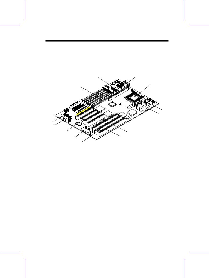
1.2.1System Board Layout
12 |
11 |
|
13 |
10 |
|
|
||
|
9 |
|
|
8 |
|
1 |
|
|
2 |
|
|
3 |
7 |
|
6 |
||
4 |
||
|
||
5 |
|
1 |
PS/2 keyboard connector |
8 |
CPU voltage regulator |
2 |
PS/2 mouse connector |
9 |
Buzzer |
3 |
PCI slots |
10 |
CPU socket |
4 |
Keyboard controller |
11 |
CPU voltage regulator |
5 |
EISA slots |
12 |
Cache module socket |
6 |
Video RAM |
13 |
SIMM sockets |
7 |
Video RAM upgrade socket |
|
|
Figure 1-1 System Board Layout
System Board |
1-3 |

1.3Jumpers and Connectors
1.3.1Jumper and Connector Locations
Figure 1-2 shows the jumper locations on the system board. The blackened pin on a jumper represents pin 1.
Figure 1-2 Jumper Locations
Jumpers are prefixed “JP”. Connectors are prefixed “CN”. FA1 to FA5 are fan connectors.
The blackened pin of a jumper represents pin 1.
1-4 |
User’s Guide |

1.3.2Jumper Settings
Table 1-1 |
Jumper Settings |
|
||
|
|
|
|
|
|
Jumper |
|
Setting |
Function |
|
CPU Voltage |
|
|
|
|
JP1 |
|
1-2 |
VR |
|
|
|
2-3* |
VRE |
|
Cache Size |
|
|
|
|
JP3 |
|
1-2* |
256 KB |
|
|
|
2-3 |
512 KB |
|
|
|
|
|
|
BIOS Version |
|
|
|
|
JP8 |
|
1-2* |
Acer |
|
|
|
2-3 |
Generic |
|
Password Security |
|
|
|
|
JP9 |
|
1-2 |
Enabled |
|
|
|
2-3* |
Bypass |
|
PC Sound Source |
|
|
|
|
JP10 |
|
1-2* |
Buzzer |
|
|
|
2-3 |
Speaker |
|
|
|
|
|
|
Front Panel Reset |
|
|
|
|
JP11 |
|
1-2* |
Enabled |
|
|
|
2-3 |
Disabled |
|
CPU Type |
|
|
|
|
JP17, JP18, JP19 |
1-2 |
P55C CPU |
|
|
|
|
2-3* |
P54C CPU |
|
SCSI Selection |
|
|
|
|
JP20 |
|
1-2* |
PCI device ID is 11 Hex |
|
|
|
2-3 |
PCI device ID is 0C Hex |
|
|
|
4-5 |
Disabled |
|
|
|
|
|
|
Onboard VGA |
|
|
|
|
JP23 |
|
1-2* |
Enabled |
|
|
|
2-3 |
Disabled |
*Default setting
System Board |
1-5 |

Table 1-1 |
Jumper Settings |
(continued) |
|
|
|
||||
|
|
|
|
|
|
|
|
|
|
|
Jumper |
|
|
Setting |
|
|
Function |
|
|
|
SCSI Termination |
|
|
|
|
|
|
|
|
|
JP24 |
|
1-2* |
|
High-byte terminator ON |
|
|||
|
|
|
2-3 |
|
|
High-byte terminator OFF |
|||
|
Core/Bus Freq. |
|
JP4 |
JP5 |
JP7 |
Bus Freq. |
Core Freq. |
Ratio |
|
|
JP4, JP5, JP7 |
2-3 |
2-3 |
1-2 |
50 MHz |
75 |
MHz |
3/2 |
|
|
|
|
1-2 |
1-2 |
2-3 |
60 MHz |
150 |
MHz |
5/2 |
|
|
|
2-3 |
1-2 |
2-3 |
60 MHz |
120 |
MHz |
2/1 |
|
|
|
2-3 |
2-3 |
2-3 |
60 MHz |
90 |
MHz |
3/2 |
|
|
|
1-2 |
2-3 |
3-4 |
66 MHz |
200 |
MHz |
3/1 |
|
|
|
1-2 |
1-2 |
3-4 |
66 MHz |
166 |
MHz |
5/2 |
|
|
|
2-3 |
1-2 |
3-4 |
66 MHz |
133 |
MHz |
2/1 |
|
|
|
2-3 |
2-3 |
3-4 |
66 MHz |
100 |
MHz |
3/2 |
|
|
|
|
|
|
|
|
|
|
1-6 |
User’s Guide |

1.3.3Connector Functions
Table 1-2 lists the different connectors on the system board and their respective functions.
Table 1-2 |
Connector Functions |
||
|
|
|
|
|
Connector |
Function |
|
|
CN1 |
|
COM1 |
|
|
|
|
|
CN2 |
|
COM2 |
|
|
|
|
|
CN3 |
|
Power connector for 200-watt SPS |
|
|
|
|
|
CN4 |
|
Power connector for 300-watt SPS |
|
|
|
|
|
CN5 |
|
Parallel port connector |
|
|
|
|
|
CN6 |
|
Diskette drive connector |
|
|
|
|
|
CN7 |
|
IDE drives connector |
|
|
|
|
|
CN8 |
|
Remote diagnostic module (RDM) connector |
|
|
|
|
|
CN9 |
|
Remote diagnostic module (RDM) connector |
|
|
|
|
|
CN10 |
|
Faulty-drive LED connector |
|
|
|
|
|
CN11 |
|
Fast SCSI-II (narrow SCSI) connector |
|
|
|
|
|
CN12 |
|
Wide SCSI connector |
|
|
|
|
|
CN13 |
|
VGA daughter board connector |
|
|
|
|
|
CN15 |
|
Power LED and keylock connector |
|
|
|
|
|
CN16 |
|
Hard disk LED connector |
|
|
|
|
|
CN17 |
|
Speaker connector |
|
|
|
|
|
CN18 |
|
Reset/Turbo connector |
|
|
|
|
System Board |
1-7 |

1.4ESD Precautions
Always observe the following ESD (electrostatic discharge) precautions before installing any system component:
1.Do not remove any system component from its packaging unless you are ready to install it.
2.Wear a wrist grounding strap before handling electronic components. Wrist grounding straps are available at most electronic component stores.
DO NOT attempt the procedures in the following sections unless you are confident of your capability to perform them. Otherwise, ask a service technician for assistance.
1-8 |
User’s Guide |
Loading...