


Acer |
Service Manual |
Service Manual
LCD Monitor Acer
AL1917W
- 0 -

1
Service Manual Versions and Revision
No. |
Version |
Release Date |
Revision |
1 |
1.0 |
2006/07/20 |
Initial Release |
|
|
|
|
Copyright
Copyright 2006 InnoLux Tech. Corp. Ltd
All Rights Reserved
This manual may not, in whole or in part, be copied, Photocopied, reproduced, translated, or converted to any electronic or machine readable form without prior written permission of InnoLux Tech. Corp. Ltd.
Acer AL1917W Service Manual
1

Acer |
Service Manual |
|
|
Table of Contents |
|
CHAPTER 1- PRECAUTIONS & SAFETY NOTICES..................................................................................................................... |
3 |
|
1. |
SAFETY PRECAUTIONS ............................................................................................................................................................ |
3 |
2. |
PRODUCT SAFETY NOTICE...................................................................................................................................................... |
3 |
3. |
SERVICE NOTES.......................................................................................................................................................................... |
3 |
CHAPTER 2- SERVICE TOOLS & EQUIPMENT REQUIRED ..................................................................................................... |
4 |
|
CHAPTER 3- CIRCUIT THEORY ...................................................................................................................................................... |
5 |
|
2. INTERFACE BOARD DIAGRAM ................................................................................................................................................... |
5 |
|
3. ELECTRONIC CIRCUIT THEORY.......................................................................................................................................................... |
6 |
|
CHAPTER 4- DISASSEMBLY & ASSEMBLY................................................................................................................................... |
9 |
|
1. EXPLODED DIAGRAM ........................................................................................................................................................................ |
9 |
|
2. DISASSEMBLY BLOCK ..................................................................................................................................................................... |
10 |
|
3. ASSEMBLY BLOCK........................................................................................................................................................................... |
11 |
|
CHAPTER 5- TEST AND ADJUSTMENT........................................................................................................................................ |
12 |
|
1. |
GENERALPOINTS............................................................................................................................................................... |
12 |
1.1 |
TEST EQUIPMENT OR TOOL................................................................................................................................................ |
12 |
1.2 |
PRESET TEST PATTERN ....................................................................................................................................................... |
12 |
1.3 |
AC INPUT............................................................................................................................................................................. |
12 |
1.4 |
OBSERVATION DISTANCE .................................................................................................................................................... |
12 |
1.5 |
KEY FUNCTION DESCRIPTION ............................................................................................................................................ |
12 |
1.6 |
BURN-IN (AGING) PATTERN ................................................................................................................................................ |
13 |
1.7 |
WARM UP............................................................................................................................................................................. |
13 |
2. |
INPUT SIGNAL...................................................................................................................................................................... |
13 |
2.1 |
VIDEO SIGNAL INPUT.......................................................................................................................................................... |
13 |
3. |
FUNCTION CHECK ............................................................................................................................................................. |
15 |
3.1 |
OSD FUNCTION TEST ......................................................................................................................................................... |
15 |
3.2 |
SCREEN PICTURE CHECK ................................................................................................................................................... |
15 |
3.3 |
AUTO COLOR BALANCE...................................................................................................................................................... |
15 |
3.4 |
TIMING CHECK ................................................................................................................................................................... |
15 |
3.5 |
POWER CONSUMPTION FUNCTION TEST............................................................................................................................ |
15 |
3.6 |
VGACABLE DETECT TEST................................................................................................................................................. |
16 |
3.7 |
HI-POT TEST........................................................................................................................................................................ |
16 |
3.8 |
GROUNDING TEST ............................................................................................................................................................... |
16 |
3.9 |
BUMPING TEST .................................................................................................................................................................... |
16 |
4. |
DISPLAY CHECK.................................................................................................................................................................. |
16 |
4.1 |
PANEL FLICKER CHECK...................................................................................................................................................... |
16 |
4.2 |
PANEL DEFECT INSPECTION ............................................................................................................................................... |
16 |
5. |
PICTURE CHECK................................................................................................................................................................. |
17 |
5.1 |
CHECK BRIGHTNESS UNIFORMITY...................................................................................................................................... |
17 |
5.2 |
COLOR TEMPERATURE CHECK .......................................................................................................................................... |
18 |
5.3 |
BRIGHTNESS OUT (VIDEO SIGNAL INPUT 700MV ± 2%).................................................................................................... |
19 |
5.4 |
DDC DATA CHECK.............................................................................................................................................................. |
19 |
CHAPTER 6- TROUBLE SHOOTING.............................................................................................................................................. |
20 |
|
1. NO POWER & LED OFF................................................................................................................................................................... |
20 |
|
ATTACHMENT 1- BILL OF MATERIAL......................................................................................................................................... |
27 |
|
PCBA P+I .............................................................................................................................................................................................. |
27 |
|
ATTACHMENT 2- SCHEMATIC....................................................................................................................................................... |
33 |
|
ATTACHMENT 3- PCB LAYOUT ..................................................................................................................................................... |
41 |
|
2

Acer |
Service Manual |
|
Chapter 1- PRECAUTIONS & SAFETY NOTICES |
1. SAFETY PRECAUTIONS
This monitor is manufactured and tested on a ground principle that a user’s safety comes first. However, improper used or installation may cause damage to the monitor as well as to the user.
WARNINGS:
This monitor should be operated only at the correct power sources indicated on the label on the rear of the monitor. If you’re unsure of the power supply in you residence, consult your local dealer or Power Company.
Do not try to repair the monitor by yourself, as it contains no user-serviceable parts. This monitor should only be repaired by a qualified technician.
Do not remove the monitor cabinet. There are high-voltage parts inside that may cause electric shock to human bodies.
Stop using the monitor if the cabinet is damaged. Have it checked by a service technician.
Put your monitor only in a lean, cool, dry environment. If it gets wet, unplug the power cable immediately and consult your closed dealer.
Always unplug the monitor before cleaning it. Clean the cabinet with a clean, dry cloth. Apply non-ammonia based cleaner onto the cloth, not directly onto the class screen.
Do not place heavy objects on the monitor or power cord.
2.PRODUCT SAFETY NOTICE
Many electrical and mechanical parts in this chassis have special safety visual inspections and the protection afforded by them cannot necessarily be obtained by using replacement components rated for higher voltage, wattage, etc. Before replacing any of these components read the parts list in this manual carefully. The use of substitute replacement parts, which do not have the same safety characteristics as specified in the parts list, may create shock, fire, or other hazards.
3.SERVICE NOTES
When replacing parts or circuit boards, clamp the lead wires around terminals before soldering.
Keep wires away from high voltage, high temperature components and sharp edges.
Keep wires in their original position so as to reduce interference.
Adjustment of this product please refers to the user’ manual.
3

Acer |
Service Manual |
|
Chapter 2- SERVICE TOOLS & EQUIPMENT REQUIRED |
1.SIGNAL GENERATOR
2.MULTIMETER
3.SCREW DRIVER
4.OSCILLOSCOPE
5.Soldering IRON
6.SOLDER
7.VGA Cable (15pins point to point)
8.DVI Cable(DVI-D 24+1 pin)
9.Color Analyzer
10.Mstar ISP Board
11.EDID Board
12.EDID program file
4
Acer |
Service Manual |
Chapter 3- CIRCUIT THEORY
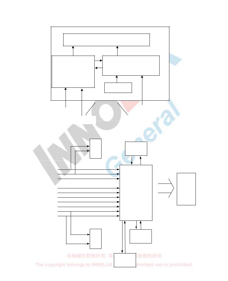
1. Monitor Block Diagram
The LCD Monitor contains an interface board, and inverter/power/Audio board, keypad board and flat panel. In Inverter/power/Audio board, power section supplies +14V & +5V for Inverter/Audio and Interface board used. The inverter section drives the backlight of panel and the DC-DC conversion. The Audio section drives speaker (2 x1W).
Flat panel (LVDS interface) and CCFL |
|
Inverter/Power |
|
(Including AC/DC Power |
Interface Board |
Supply , Inverter ) |
|
|
Keypad BD |
AC input |
|
|
Host computer |
Range 100V~240V |
|
|
(VGA/DVI signal input and DDC) |
|
|
|
|
|
|
|
|
Audio input
2. Interface BOARD DIAGRAM
5

Acer |
Service Manual |
3.Electronic Circuit Theory
3.1Switching Mode Power Supply
3.1.1 AC Current Input Circuit
P801 is a connector for connecting AC Power. F801 is a fuse to protect all the circuit. AC input voltage is from 90v to 264V. R801 and R802 joined between two inputting main circuit to prevent man from shock. L801 is used to clear up low frequency wave. C801 and C802 are used to discharge the waves that L801 produced. High frequency waves are damped by C801 and C802. D801 is a rectifier which composed of 4 build-in diodes, it inverts AC to DC.
3.1.2 High Voltage to Low Voltage Control Circuit
C804 is used to smooth the wave from rectifier. IC802 is a highly integrated PWM controller. When rectified DC high voltage is applied to the HV pin during start-up, the MOSFET Q804 is initially off, and the Vcc pin capacitor is charged. When the Vcc pin voltage reaches approximately 10V, the control circuitry is activated and the soft-start begins. The soft-start circuit gradually increases the duty cycle of the MOSFET from zero to the maximum value over approximately 4ms. If no external feedback/supply current is fed into the FB pin by the end of the soft-start, the current Setpoint will be above the fault level, FAULT flag is raised, if the FAULT duration exceeds 80ms, the output controller disable
Resistor R808, R809, R810, R811 are for line over voltage shutdown(OVP)
When PWM is turned off, the main current flow will be consumed through R804 and D802, This will prevent MOSFET Q804 from being damaged under large current impulse and voltage spike.
D803 and C807 to provide internal Auxiliary voltage to Vcc pin during normal operation. Otherwise, error amplifier and feedback current input the FB pin for duty cycle control.
3.1.3 DC_5V and DC_14V Output Circuit
For DC 5V, D805 is used to rectify the inducted current. R828 and C814 are used to store energy when current is reversed. The parts including C818, C822, C820,L803 are used to smooth the current waves.
For DC 14V, D803 is used to rectify the inducted current. R827 and C813 are used to store energy when current is reversed. The parts including C815, C817 and L802 are used to smooth the current waves.
3.1.4 Feedback and OVP Protect Circuit
Pin R of IC803 is supplied 2.5-v stable voltage. It connects to 5V and 14V output through R822, R823 and R824. R822, R823 and R824 are output sampling resistor. When the sampling voltage more than 2.5V or less than 2.5V, current of FB IC802 will change, this can change the voltage from T801.
OVP Protect Circuit: When output is overvoltage, the auxiliary winding voltage will be increased, when it reaches about 14V. Q803 is triggered . It makes the IC802 Pin 1 exceed 5V, then the IC802 output will be disabled.
Q801, R816, R817 and ZD803 make up of dummy loading circuit. For start-up sequence, during 5V output take place high loading first, this dummy loading circuit operated to insure 14V not be increased.
3.2 I/F Board Circuit
3.2.1 RGB CAPTURE
-Signal RED,GREEN,BLUE input through CN103 #1,#2,#3, Stop DC via C112, C114 and C116, and then enter into U105 (scaler) analog input terminal #18,#20,#23, and then scaler deals with signal internally. TVS101, TVS102, TVS103 are ESD protector to prevent U105 from ESD.
-Signal DDC_SCL (series clock) inputs via CN103#15, and then passes through ZD101 Zener for ESD protection, goes into U105 #31.
-Signal DDC_SDA (series data) inputs via CN103#12, and then passes through ZD107 Zener for ESD protection, goes into U105 #30.
-Signal TTL vertical sync. (Vsync) inputs via CN103 #14, and then clamped by ZD105 Zener, passes through R129, and then goes into IC U105 (scaler) #28.
6

Acer |
Service Manual |
-Signal TTL horizontal sync. (Hsync) inputs via CN103 #13, and then clamped byZD106 Zener, passes through FB101,R130, and then goes into IC U105 (scaler) #27.
-CN103#5 is defined as cable detect pin, this detector realize passes through R122 Pull hight, go into U105#35.
-U103 power is supplied by PC via CN103#9, or supplied by Monitor self via D103.
-U103 is an EEPROM IC which is memory and EDID data saved in it.
3.2.2 Buttons Control
-Button “Power” on right side bezel connects to U105 (scaler) #88 through R161, via CN105#4.
-Button “UP” “DOWN ““MENU” “AUTO” on right side bezel connects to U105 (scaler) #89,#88,#89,#88 through R158,R159,R160,R157,via CN105 #6, #5.
-U108 is an EEPROM IC which memory OSD setting and save the value adjusted by user.
-LED Indicator on Front Bezel
a.When press button “power”, U105 (scaler) #42 sends out a low potential, via R101, flow to CN105 #2 on keypad, LED Green ON.
b.When in “Suspend” mode, U105 (TSUM56AL) #41 sends out a low potential, via R107, flows to CN105 #1 on keypad, LED Amber ON.
3.2.3 Mstar CHIP U105 (scaler)
-U105 (TSUM56AL-1& TSUM16AL-1) #54. #55. #58~#65 output 8 bit even LVDS digital data to panel control circuit through CN104.
-U105 (TSUM56AL) #67~#74. #77. #78 output 8 bit odd LVDS digital data to panel control circuit through CN104.
-U105 (TSUM56AL-1& TSUM16AL-1) #86 outputs Brightness “PWM” signals to control CCFL brightness.
-U105 (TSUM56AL-1& TSUM16AL-1) #48 output PPWR ”H” potential to make Q103 conducted, and then make Q101 conducted, +5V flow to CN104#1~#3 as Panel VDD .
-U105 (TSUM56AL-1& TSUM16AL-1) #85 output CCFL_ON/OFF ”H” potential to control Inverter on/off.
-TCLK by Crystal 14.318MHz input to U105 (TSUM56AL-1& TSUM16AL-1) #96,#97.
Please refer to TSUM56AL Pin Assignments table in page
3.2.4 Regulator Circuit
-+5V is from switching mode power supply for Panel used.
-+3.3V generates from +5V through C101 and C103 filtering and U101 which is output +3.3V LDO for U103, U106,U108 and U105 used.
-+1.8V generates from +5V through C101 and C103 filtering and U102 which is output +1.8V LDO, for U105 used.
3.2.5 Audio circuit
-Audio Signal R,L,GND input through P701,#2,#5,#1, Stop DC via C711, C712, and then enter into U701 (TDA7496L) analog input terminal #4,#9.
-U701 (TDA7496L) #14,#17 output R,L audio data to Speaker through CN701.
-U105 (TSUM56AL) #94 output MUTE “H” potential to control U701on/off.
-U105 (TSUM56AL) #93 outputs Volume “PWM” signals to control U701 Volume.
4.Inverter circuit
1. R503, ZD501, R502, Q501 components convert +14V voltage into +5.0V voltage, and the voltage supply to IC501. The extra PWM pulse signal (BRIGHTNESS signal) input to control IC through R512, R514, C510, The LCT pin is set to a DC voltage of 0.7V by using a resistor divider(R507, R516), change the duty of PWM pulse, will regulate the lamp current. The ON/OFF voltage connect to pin10 of IC501 through D501, R501, A voltage of 2V to pin10 of IC501 enables the IC and activates the striking timer. The SSTCMP pin of IC501 performs the soft function, the C511 set the time of SST. The operation frequency determined by external capacitor C512, C521 and resistor R508 connected at CT pin of IC501. C515 connect the TIMER pin of IC501, the capacitor to set striking time and shunt down delay time. DRV!, DRV2 output
7

Acer |
Service Manual |
for power MOSFET U501, U502.
2.OZ9938 provides two drive signals for U501, U502, and they work in push pull topology driving, two transformers are connected in parallel with each transformer driving two lamps in series. Turning each N-Channel MOSFET “on/off” complementarily, produces an alternating current through the transformer primary and secondary. The “on” duration of the switches determines the amount of energy delivered to the CCFLs. R504, C504, R505, C505, R532, C529, R530, C522 are snubber networks, they suppress Voltage transient spike in drain of power MOSFET.
3.R506, R510, C509, C513, C514, R525, R531, C528, C525, and C527 are connected between high voltage output connector and ground, the divided AC voltage is inverted DC voltage through D502, D503, D508, and D509. The sense voltage feed back to VSEN (pin 6 of IC501) for an over voltage/over current condition during normal operation. R528, R533 are current sense resistor, current sense signal feed back to Isense (pin 5 of IC501) for lamp “ON” detection.
8

Acer |
Service Manual |
Chapter 4- Disassembly & Assembly
1. Exploded Diagram
9 |
Acer |
Service Manual |
2. Disassembly Block |
|
AL1917W
LCD Monitor
ASSY, BASE
BASE*1
RUBBER FOOT *4
GASKET*1
PLATE,BASE*1
T4*6,Zn, ROHS *2
HINGE COVER*1
CHASSIS *1
PCBA I/F BOARD *1 PCBA INV.&DC-DC *1 KEY PAD*1
HRN ASS'Y 8P
CABLE 30P FFC SPEAKER*1 BOLT,#4-40x11.8,Ni ROHS *2(W/O DVI )or 4(W/DVI) M3*5, Ni ROHS *4,
P, W-SPR ,M3*6,Zn,ROHS*1 MYLAR *4
BRACKET FINGER *1 HINGE *1
STAND*1
SCREW,B,CROSS,W/W-SPR,M4*20,Zn ROHS *3
ASSY STAND
M4*8,Black Zn,NL ROHS *4
ASSY FRONT BEZEL
BACK COVER
SCREW, P, T3*8,Zn,ROHS*1
FRONT BEZEL *1 FUNCTION KEY *1 POWER BUTTON *1
LED LENS
ASSY PANEL UNIT |
|
|
M3*4, Zn,ROHS *4 |
|
PANEL INNOLUX |
|
M190A1-L01 |
|
TAPE,MYLAR*1 |
|
|
|
|
|
|
|
|
|
|
|
Note:
The DIS-assembly direction please following direction of arrowhead
10
Acer |
Service Manual |
3. Assembly Block
|
|
|
PCBA Power *1 |
|
|
||
|
|
|
SCREW PW,CROSS,W/WAS, M3*5,NI*3 |
|
|
||
|
|
SCREW,P,CROSSW/W-SPR,M3*6,Zn,ROHS*1 |
|
|
|||
|
|
|
SPEAKER*1 |
|
|
||
|
|
|
|
|
|
|
|
PCBA I/F BOARD *1 |
|
|
|
|
|
|
|
|
|
|
|
|
|
||
CABLE 30 PIN FFC |
|
|
|
|
|
|
|
|
|
|
|
|
PANEL INNOLUX |
|
|
SCREW,PW,CROSS,W/WAS, |
|
|
|
|
|
|
|
|
|
|
|
|
|
||
M3*5,NI*1 |
|
|
|
|
|
M190A1-L01 |
|
BOLT,#4-40x11.8,Ni ROHS |
|
|
|
|
|
|
|
|
|
ASSY PANEL*1 |
|
|
|
||
*2(W/O DVI )or 4(W/DVI) |
|
|
|
|
|
||
|
|
SCREW,P,CROSS,W/WAS, |
|
|
|
||
|
|
|
|
|
|
||
|
|
|
M3*4,Zn*4 |
|
CHASSIS *1 |
|
|
|
|
|
TAPE,MYLAR*1 |
|
|
||
|
|
|
|
MYLAR*4 |
|
||
|
|
|
|
|
|
|
|
|
|
|
|
|
|
|
|
KEY PAD*1
HRN ASS'Y 8P*1
KEY PAD*1
HRN ASS'Y 8P*1
ASSY BEZEL*1
STAND*1
HINGE*1
BRACKET FINGER*1 ASSY STAND*1
SCREW,B,CROSS,W/W-SPR,M4*  M4*8,Black Zn,NL ROHS *4 20,Zn ROHS *3
BASE*1
RUBBER*4 ASSY BASE*1
GASKET*1
PLATE,BASE*1
T4*6,Zn, ROHS *2
BEZEL*1
BUTTON,POWER KEY*1
BUTTON,FUNCTION*1
LENS*1
HINGE COVER*1
LE 1954
LCD Monitor
11

Acer |
Service Manual |
Chapter 5- TEST AND ADJUSTMENT
1.GENERAL POINTS
1.1Test Equipment or Tool
1.1.1Test pattern generator: PC or video pattern generator (Chroma-2326/2160/2130)
1.1.2Color analyzer: Chroma-7120
1.1.3Power meter: AC Source Chroma-6408
1.1.4Electrical safety tester: Chroma (Zentech) 9032A
1.1.5Stereo source: Music or signal generator input
1.1.6Auto shock fixture
1.1.7Temperature and humidity sensor
1.1.8DDC interface card and EDID file
1.2Preset Test Pattern
1.2.1Crosshatch (General-1)
1.2.2Gray Bar (16 & 32 levels)
1.2.3Full White
1.2.4Aging (Burn-in) Pattern: Full Red, Green, Blue, White, and Black
1.3AC input
All measurements mentioned hereafter are carried out at a normal mains voltage (90 - 264 VAC for the model with full range power supply, unless otherwise stated)
1.4Observation Distance
1.4.1Observation distance from eyes to panel is defined as 50cm
1.4.2Visual distance from instrument to panel is defined as 20cm
1.5Key Function Description
1.5.1 Control buttons on the front bezel
|
|
CONTROL |
|
|
|
|
|
|
KEYS FUNCTION |
|
|||
|
|
KEY |
|
|
|
|
|
|
|
||||
|
|
|
|
|
|
|
|
|
|
|
|
|
|
|
|
[AUTO] |
|
|
A. When OSD un-displays, press [AUTO] to perform auto-adjustment |
||||||||
|
|
|
|
B. When OSD displays, press [AUTO] to return to previous level menu |
|||||||||
|
|
|
|
|
|||||||||
|
|
|
|
|
|
|
|
|
|
|
|
||
|
|
|
|
|
A. When OSD isn’t shown on screen, press [MENU] to enter OSD interface |
||||||||
|
|
[MENU] |
|
|
B. When OSD displays, press [MENU] to perform function of menu icon that is |
||||||||
|
|
|
|
|
highlight or enter next level menu |
||||||||
|
|
|
|
|
|
|
|
|
|
|
|
||
|
|
|
|
|
A. When “MENU OSD” displays, press these keys to change the contents of an |
||||||||
|
|
[►], [◄] |
|
|
adjustment item, or change an adjustment value |
||||||||
|
|
|
|
B. When “MENU OSD” un-displays, press [►],adjust volume high; |
|||||||||
|
|
|
|
|
|||||||||
|
|
|
|
|
press [◄]adjust volume low |
|
|
|
|||||
|
|
[POWER] |
|
|
Power on or power off the monitor |
|
|
|
|||||
|
|
|
|
|
|
|
|
|
|
|
|
|
|
|
|
1.5.2 Hot Key Operation |
|
|
|
|
|
|
|
||||
|
|
|
|
|
|
|
|
|
|
|
|
|
|
|
|
|
|
|
|
|
HOT KEY OPERATION |
|
|
|
|||
|
|
FUNCTION |
|
|
|
|
|
|
|
|
|
DESCRIPTION |
|
|
|
AUTO |
|
◄ |
► |
MENU |
POWER |
|
|||||
|
|
|
|
|
|
||||||||
|
|
|
|
|
|
|
|
|
|
|
|
|
|
|
|
|
|
|
|
|
|
|
|
|
|
Press [AUTO] & [MENU] at the same |
|
|
|
FACTORY |
|
|
|
|
|
|
|
|
|
time, and then press [POWER] for DC |
|
|
|
|
|
● |
|
|
|
● |
|
ON |
power on. OSD menu will be shown |
|
|
|
|
MODE |
|
|
|
|
|
|
|
||||
|
|
|
|
|
|
|
|
|
|
|
with “F” on the left top. Select “F” for |
|
|
|
|
|
|
|
|
|
|
|
|
|
|
|
|
|
|
|
|
|
|
|
|
|
|
|
|
entering factory mode. |
|
|
|
|
|
|
|
|
|
|
|
|
|
|
|
12
Acer |
Service Manual |
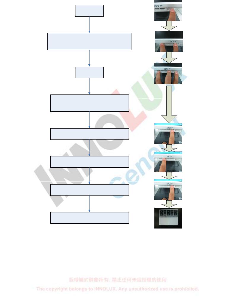
1.5.3 Process To Access Factory Mode
Power Off
Press “AUTO”& ”MENU”button at
the same time
Power On
Release the “AUTO”& ”MENU”
button
Press “MENU” Button
Press “<” Button
Press “Menu” Button
Enter the factory Mode
1.6Burn-in (Aging) Pattern
1.6.1Burn-in patterns are: full Red, Green, Blue, White and Black
1.6.2Stop burn-in pattern by providing with video signal from D-sub or DVI-D connector
1.7Warm Up
All test units have to be done warm up after at least 2 hours in a room with temperature of 40±5°C. (Except particular requirement)
2.INPUT SIGNAL
2.1Video Signal Input
13
 Loading...