


HCD-ZUX999
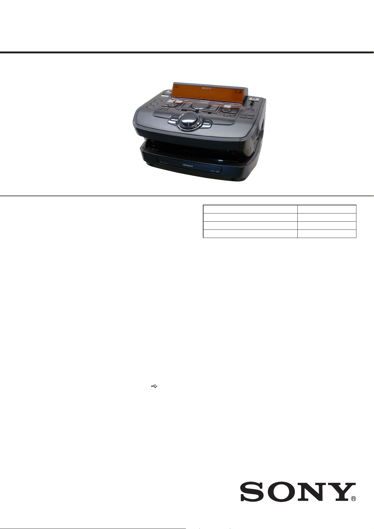
HCD-ZUX999
SERVICE MANUAL
Ver. 1.0 2009.07
• HCD-ZUX999 is the tuner, CD, USB and
amplifi er section in FST-ZUX999.
• “WALKMAN” and “WALKMAN” logo are registered trademarks of
Sony Corporation.
• “Memory Stick” is a trademark of Sony Corporation.
• MPEG Layer-3 audio coding technology and patents licensed from
Fraunhofer IIS and Thomson.
• Windows Media is a registered trademark of Microsoft Corporation
in the United States and/or other countries.
E Model
Model Name Using Similar Mechanism New
Mechanism Type CDM74KF-F2BD82F-A
Base Unit Name BU-F2BD82F-A
Optical Pick-up Name KSM-215DHAP
Amplifi er section
The following measured at AC 127 V, 60 Hz
(Mexican model)
The following measured at AC 120, 220,
240 V, 50/60 Hz (Other models)
Front/Rear speaker:
Power output (rated):
160 W + 160 W (at 6 Ω, 1 kHz,
1% THD)
RMS output power (reference):
250 W + 250 W/250 W + 250 W
(per channel at 6 Ω, 1 kHz, 10%
THD)
Inputs
AUDIO IN 1, 2 L/R:
voltage 250 – 700 mV, impedance
47 kilohms
MIC: sensitivity 1 mV, impedance
10 kilohms
SPECIFICATIONS
Outputs
i (Headphones):
accepts headphones with an
impedance of 8 Ω or more
FRONT/REAR SPEAKER:
Use only the supplied speaker
SS-ZUX999
USB section
Supported bit rate:
MP3 (MPEG 1 Audio Layer-3):
32 – 320 kbps, VBR
WMA: 48 – 192 kbps, VBR
AAC: 48 – 320 kbps
Sampling frequencies:
MP3 (MPEG 1 Audio Layer-3):
32/44.1/48 kHz
WMA: 44.1 kHz
AAC: 44.1 kHz
(USB 1 and USB 2) port: Type A
Maximum current: 500 mA
CD player section
System:
Compact disc and digital audio
system
Laser Diode Properties
Emission duration: Continuous
Laser Output*: Less than 44.6μW
* This output is the value measurement
at a distance of 200mm from the
objective lens surface on the Optical
Pick-up Block with 7mm aperture.
Frequency response:
20 Hz – 20 kHz
Tuner section
FM stereo, FM/AM superheterodyne tuner
Antenna:
FM lead antenna
AM loop antenna
– Continued on next page –
9-889-579-01
2009G04-1
2009.07
©
COMPACT DISC RECEIVER
Sony Corporation
Audio&Video Business Group
Published by Sony Techno Create Corporation

HCD-ZUX999
FM tuner section:
Tuning range:
87.5 – 108.0 MHz (50 kHz step)
Intermediate frequency: 10.7 MHz
AM tuner section:
Tuning range:
Latin American models:
530 – 1,710 kHz (10 kHz step)
531 – 1,710 kHz (9 kHz step)
Other models:
531 – 1,602 kHz (9 kHz step)
530 – 1,610 kHz (10 kHz step)
Intermediate frequency: 450 kHz
General
Power requirements
Mexican model:
AC 127 V, 60 Hz
Other models:
AC 120, 220 or 230 – 240 V,
50/60 Hz, adjustable with voltage
selector
Power consumption
330 W
Dimensions (w/h/d) (excl. speakers)
Approx. 506 × 342 × 513 mm
Mass (excl. speakers)
Approx. 20.0 kg
Supplied accessories: Remote Commander
(1), R6 (Size AA) batteries (2), FM lead
antenna (1), AM loop antenna (1), Speaker
cords (4)
Design and specifi cations are subject to
change without notice.
NOTES ON CHIP COMPONENT REPLACEMENT
• Never reuse a disconnected chip component.
• Notice that the minus side of a tantalum capacitor may be damaged by heat.
FLEXIBLE CIRCUIT BOARD REPAIRING
• Keep the temperature of soldering iron around 270 °C during
repairing.
• Do not touch the soldering iron on the same conductor of the
circuit board (within 3 times).
• Be careful not to apply force on the conductor when soldering
or unsoldering.
UNLEADED SOLDER
Boards requiring use of unleaded solder are printed with the leadfree mark (LF) indicating the solder contains no lead.
(Caution: Some printed circuit boards may not come printed with
the lead free mark due to their particular size)
: LEAD FREE MARK
Unleaded solder has the following characteristics.
• Unleaded solder melts at a temperature about 40 °C higher
than ordinary solder.
Ordinary soldering irons can be used but the iron tip has to be
applied to the solder joint for a slightly longer time.
Soldering irons using a temperature regulator should be set to
about 350 °C.
Caution: The printed pattern (copper foil) may peel away if
the heated tip is applied for too long, so be careful!
• Strong viscosity
Unleaded solder is more viscous (sticky, less prone to fl ow)
than ordinary solder so use caution not to let solder bridges
occur such as on IC pins, etc.
• Usable with ordinary solder
It is best to use only unleaded solder but unleaded solder may
also be added to ordinary solder.
SAFETY-RELATED COMPONENT WARNING!
COMPONENTS IDENTIFIED BY MARK 0 OR DOTTED LINE
WITH MARK 0 ON THE SCHEMATIC DIAGRAMS AND IN
THE PARTS LIST ARE CRITICAL TO SAFE OPERATION.
REPLACE THESE COMPONENTS WITH SONY PARTS
WHOSE PART NUMBERS APPEAR AS SHOWN IN THIS
MANUAL OR IN SUPPLEMENTS PUBLISHED BY SONY.
2
HCD-ZUX999
CAUTION
Use of controls or adjustments or performance of procedures
other than those specifi ed herein may result in hazardous radia-
tion exposure.
NOTES ON HANDLING THE OPTICAL PICK-UP
BLOCK OR BASE UNIT
The laser diode in the optical pick-up block may suffer electrostatic break-down because of the potential difference generated by
the charged electrostatic load, etc. on clothing and the human body.
During repair, pay attention to electrostatic break-down and also
use the procedure in the printed matter which is included in the
repair parts.
The fl exible board is easily damaged and should be handled with
care.
NOTES ON LASER DIODE EMISSION CHECK
The laser beam on this model is concentrated so as to be focused
on the disc refl ective surface by the objective lens in the optical
pickup block. Therefore, when checking the laser diode emission,
observe from more than 30 cm away from the objective lens.
Laser component in this product is capable of emitting radiation
exceeding the limit for Class 1.
This appliance is classifi ed as
a CLASS 1 LASER product.
This marking is located on the
rear exterior.
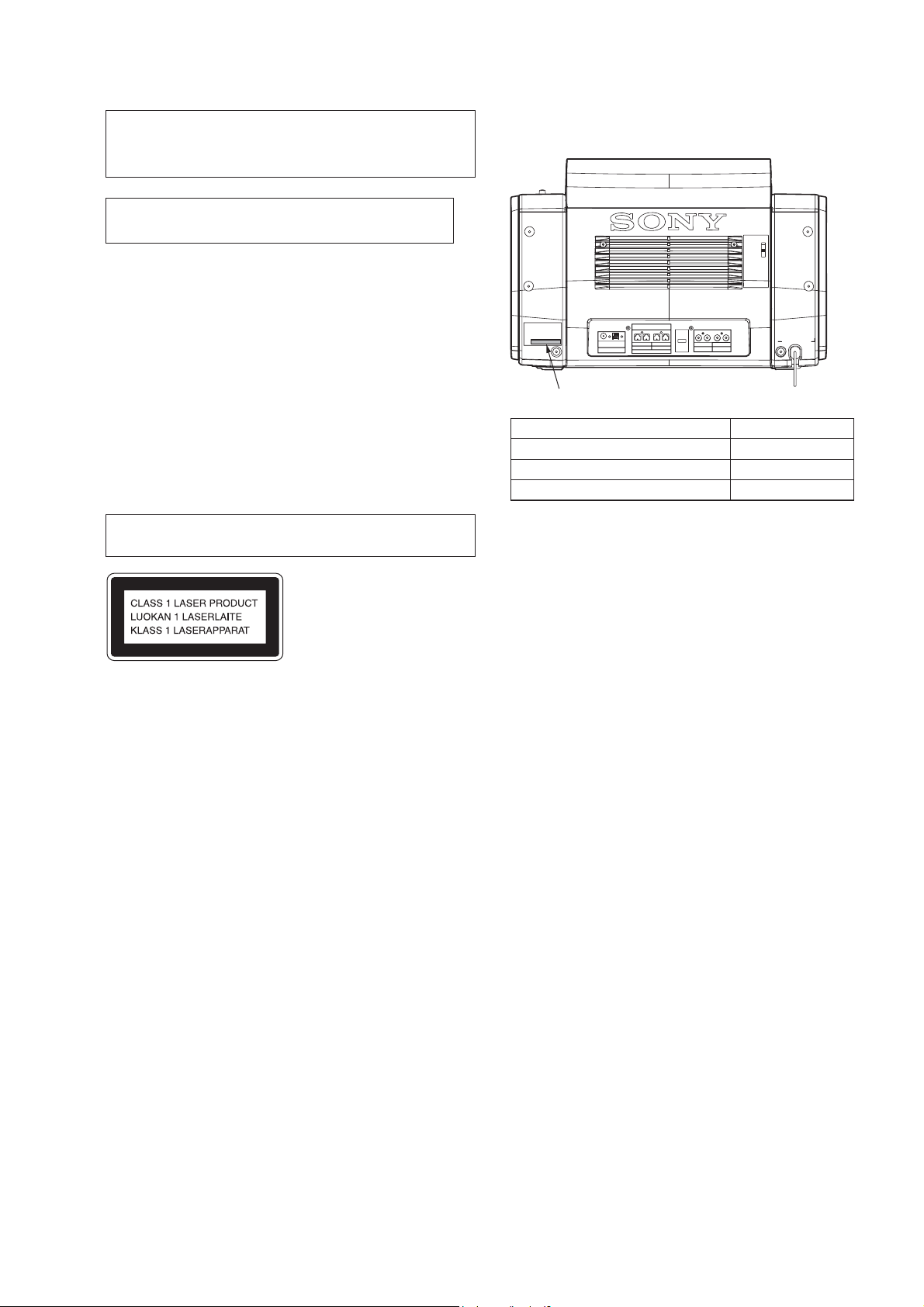
MODEL IDENTIFICATION
– Model Number Label –
Parts No.
Model Part No.
E2, E51 model
E3 model
MX model
• Abbreviation
E2 : 120V AC area in E model
E3 : 240V AC area in E model
E51 : Chilean and Peruvian models
MX : Mexican model
4-152-900-0[]
4-152-901-0[]
4-152-903-0[]
3

HCD-ZUX999
TABLE OF CONTENTS
1. SERVICING NOTES
............................................. 5
2. DISASSEMBLY
2-1. Loading Panel ................................................................ 10
2-2. Back Panel ...................................................................... 10
2-3. Top Panel Section ........................................................... 11
2-4. Side Panel (L) Assy, Side Panel (R) Assy ....................... 11
2-5. Front Panel Section ......................................................... 12
2-6. MAIN Board ................................................................... 12
2-7. CD Mechanism Deck ...................................................... 13
2-8. REGULATOR Board ...................................................... 13
2-9. PT Board, SUB PT Board ............................................... 14
2-10. AMP Board, DC FAN (FAN903).................................... 14
2-11. SPEAKER TERMINAL Board ...................................... 15
2-12. X-ROUND JOG Board ................................................... 15
2-13. RIGHT ENTER Board, LEFT ENTER Board................ 16
2-14. SH-TAS Board ................................................................ 16
2-15. PANEL FUNCTION Board ............................................ 17
2-16. LF-TUBE Board, CROSS FADER Board ...................... 17
2-17. Brackets .......................................................................... 18
2-18. MASTER VOLUME Board ........................................... 18
2-19. LEFT PANEL Board, USB-A Board .............................. 19
2-20. RIGHT PANEL Board, USB-B Board ............................ 19
2-21. BOTTOM SIRCS Board, OPEN/CLOSE KEY Board,
DISC FUNCTION Board ............................................... 20
2-22. MICROPHONE Board, HEADPHONE Board .............. 20
2-23. Base Unit ......................................................................... 21
2-24. BD Board ........................................................................ 21
2-25. DRIVER Board, SW Board ............................................ 22
2-26. SENSOR Board .............................................................. 22
2-27. MOTOR (TB) Board....................................................... 23
2-28. MOTOR (LD) Board ...................................................... 23
3. TEST MODE ............................................................ 24
4. ELECTRICAL CHECKS ...................................... 27
5. DIAGRAMS
5-1. Block Diagram –CD Servo Section– .............................. 30
5-2. Block Diagram –Audio Section– .................................... 31
5-3. Block Diagram –USB Section– ...................................... 32
5-4. Block Diagram –AMP Section– ..................................... 33
5-5. Block Diagram –Panel Section– ..................................... 34
5-6. Block Diagram –Power Section– .................................... 35
5-7. Printed Wiring Boards –Driver Section– ........................ 37
5-8. Schematic Diagram –Driver Section– ............................ 38
5-9. Printed Wiring Board –BD Section– .............................. 39
5-10. Schematic Diagram –BD Section– ................................. 40
5-11. Printed Wiring Board –Main Section– ............................ 41
5-12. Schematic Diagram –Main Section (1/4)– ...................... 42
5-13. Schematic Diagram –Main Section (2/4)– ...................... 43
5-14. Schematic Diagram –Main Section (3/4)– ...................... 44
5-15. Schematic Diagram –Main Section (4/4)– ...................... 45
5-16. Schematic Diagram –USB Section– ............................... 46
5-17. Printed Wiring Boards –SH-TAS, USB Section (1/2)– .. 47
5-18. Printed Wiring Board –SH-TAS Section (2/2)– .............. 48
5-19. Schematic Diagram –SH-TAS Section (1/5)– ................ 49
5-20. Schematic Diagram –SH-TAS Section (2/5)– ................ 50
5-21. Schematic Diagram –SH-TAS Section (3/5)– ................ 51
5-22. Schematic Diagram –SH-TAS Section (4/5)– ................ 52
5-23. Schematic Diagram –SH-TAS Section (5/5)– ................ 53
5-24. Printed Wiring Board –AMP Section–............................ 54
5-25. Schematic Diagram –AMP Section– .............................. 55
5-26. Printed Wiring Boards
–Headphone, Speaker Terminal Section–......................... 56
5-27. Schematic Diagram
–Headphone, Speaker Terminal Section– ........................ 57
5-28. Printed Wiring Board –Panel Function Section– ............ 58
5-29. Schematic Diagram –Panel Function Section (1/2)– ...... 59
5-30. Schematic Diagram –Panel Function Section (2/2)– ...... 60
5-31. Printed Wiring Boards –Left/Right Enter,
Left/Right Panel, L-Shape Illumination-A/B Section– ... 61
5-32. Schematic Diagram
–Left/Right Enter, Left/Right Panel Section– ................. 62
5-33. Schematic Diagram
–L-Shape Illumination-A/B Section– ............................. 63
5-34. Printed Wiring Boards –Cross Fader, Master Volume,
X-Round Jog Section– .................................................... 64
5-35. Schematic Diagram –Cross Fader, Master Volume,
X-Round Jog Section– .................................................... 65
5-36. Printed Wiring Boards
–Bottom Sircs, FL-Tube, Microphone Section– ............. 66
5-37. Schematic Diagram
–Bottom Sircs, FL-Tube, Microphone Section– ............. 67
5-38. Printed Wiring Boards
–Disc Function, Open/Close Key, Regulator Section– ... 68
5-39. Schematic Diagram
–Disc Function, Open/Close Key, Regulator Section– ... 69
5-40. Printed Wiring Board –Power Section– .......................... 70
5-41. Schematic Diagram –Power Section– ............................. 71
6. EXPLODED VIEWS
6-1. Overall Section ............................................................... 88
6-2. Front Panel Section ......................................................... 89
6-3. Top Panel Section-1 ........................................................ 90
6-4. Top Panel Section-2 ........................................................ 91
6-5. Top Panel Section-3 ........................................................ 92
6-6. Chassis Section ............................................................... 93
6-7. CD Mechanism Deck Section-1 ..................................... 94
6-8. CD Mechanism Deck Section-2 ..................................... 95
7. ELECTRICAL PARTS LIST .............................. 96
4
SERVICING NOTES
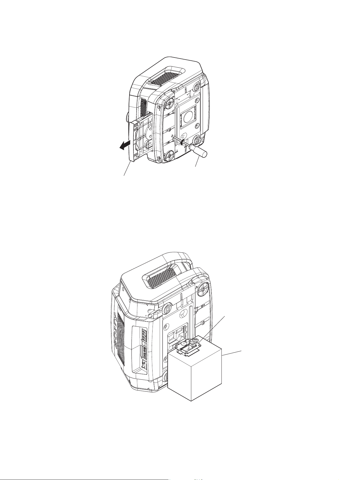
1. MANUALLY OPENING THE CD TRAY
HCD-ZUX999
SECTION 1
2
CD tray
As illustrated, insert a flathead screwdriver
and give a turn to the left to put the tray out.
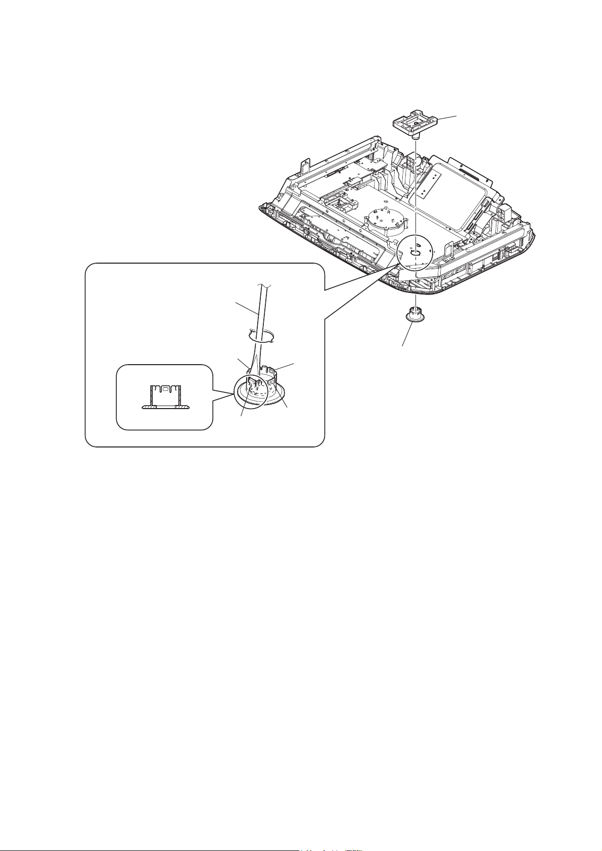
2. SERVICE POSITION OF THE BASE UNIT
1
flathead screwdriver
base unit
stand
5
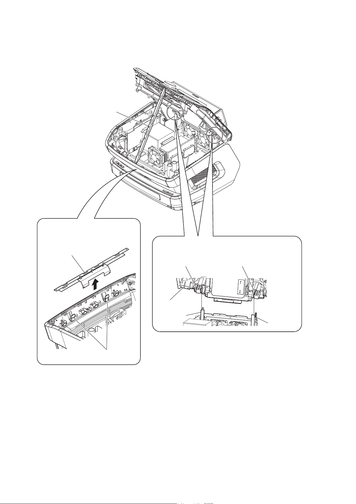
HCD-ZUX999
3. SERVICE POSITION OF THE WHOLE PLAYER
bracket (F-panel)
Removing the bracket panel (F-panel)
bracket (F-panel)
two claws
Removing the top panel section
holder (TP-support) (L)
top panel section
side bracket L
holder (TP-support) (R)
side bracket R
6
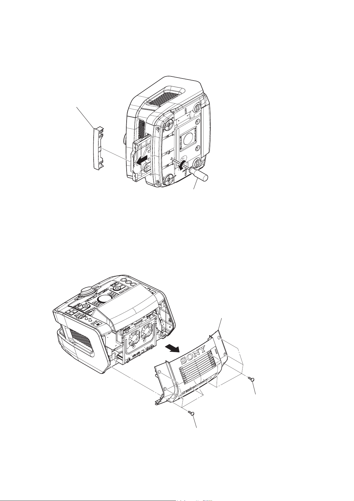
4. REMOVING THE JOG DIAL (ENTER)
2 Tap the dial with a flathead screwdriver or other tool
harder to remove it.
flathead screwdriver
HCD-ZUX999
1 BTN-enter-A-assy
claw
3 jog dial (enter)
claw
claw
claw
7
HCD-ZUX999
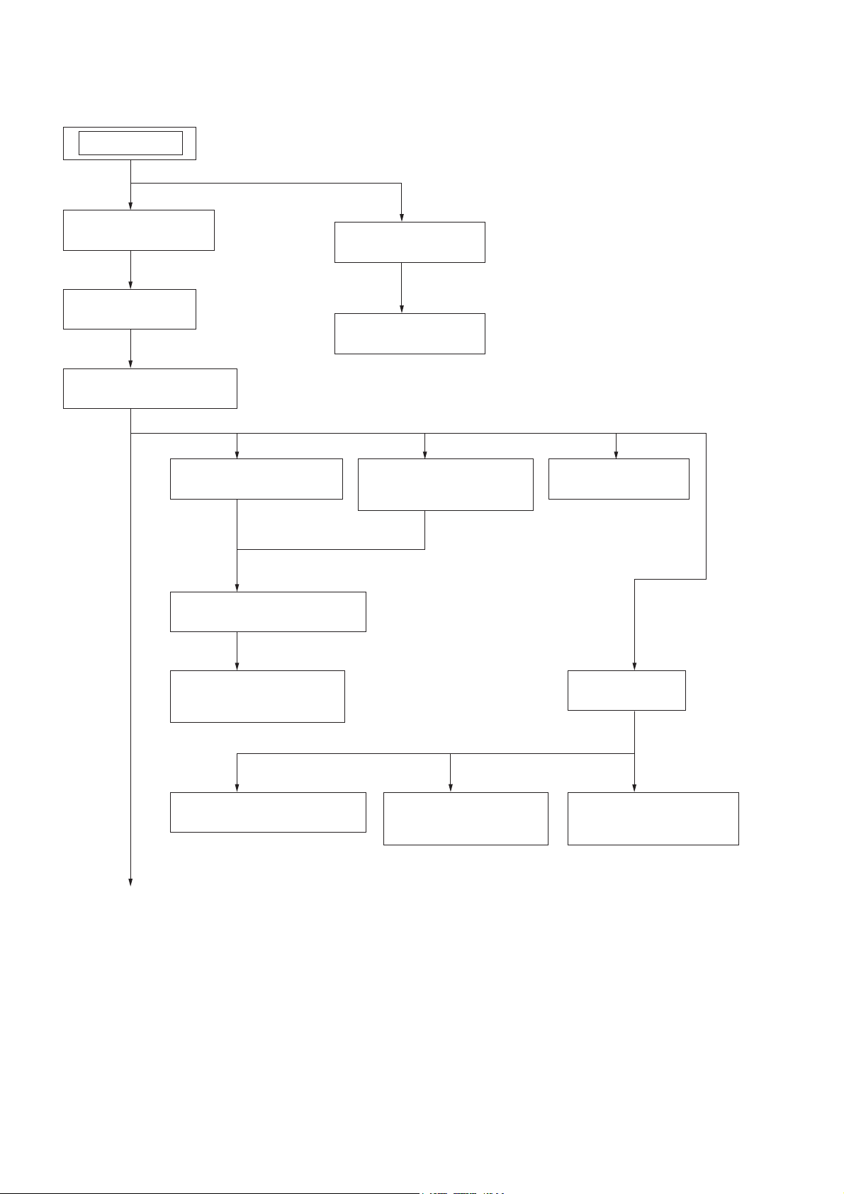
DISASSEMBLY
• This set can be disassembled in the order shown below.
SET
SECTION 2
2-1. LOADING PANEL
(Page 10)
2-2. BACK PANEL
(Page 10)
2-3. TOP PANEL SECTION
(Page 11)
2-12. X-ROUND JOG BOARD
(Page 15)
2-15. PANEL FUNCTION BOARD
(Page 17)
2-23. BASE UNIT
(Page 21)
2-24. BD BOARD
(Page 21)
2-13. RIGHT ENTER BOARD,
LEFT ENTER BOARD
(Page 16)
2-14. SH-TAS BOARD
(Page 16)
2-16. FL-TUBE BOARD,
CROSS FADER BOARD
(Page 17)
2-18. MASTER VOLUME BOARD
(Page 18)
Continued on the FLOW2
2-19. LEFT PANEL BOARD,
USB-A BOARD
(Page 19)
2-17. BRACKETS
(Page 18)
2-20. RIGHT PANEL BOARD,
USB-B BOARD
(Page 19)
8
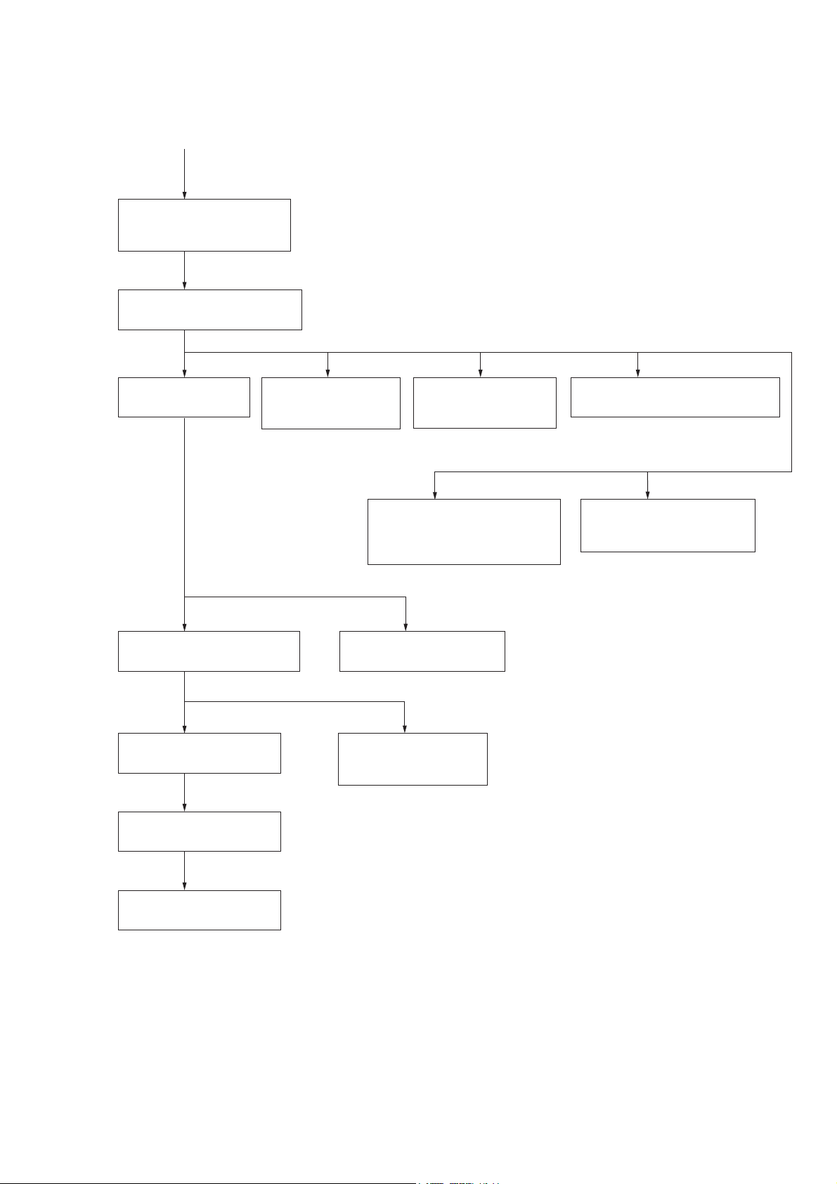
• This set can be disassembled in the order shown below.
To the FLOW1
2-4. SIDE PANEL (L) ASSY,
SIDE PANEL (R) ASSY
(Page 11)
2-5. FRONT PANEL SECTION
(Page 12)
HCD-ZUX999
2-6. MAIN BOARD
(Page 12)
2-7. CD MECHANISM DECK
(Page 13)
2-26. SENSOR BOARD
(Page 22)
2-9. PT BOARD,
SUB PT BOARD
(Page 14)
2-8. REGULATOR BOARD
(Page 13)
2-25. DRIVER BOARD,
SW BOARD
(Page 22)
2-10. AMP BOARD,
DC FAN (FAN903)
(Page 14)
2-21. BOTTOM SIRCS BOARD,
OPEN/CLOSE KEY BOARD,
DISC FUNCTION BOARD
(Page 20)
2-11. SPEAKER TERMINAL BOARD
(Page 15)
2-22. MICROPHONE BOARD,
HEADPHONE BOARD
(Page 20)
2-27. MOTOR (TB) BOARD
(Page 23)
2-28. MOTOR (LD) BOARD
(Page 23)
9
HCD-ZUX999
Note: Follow the disassembly procedure in the numerical order given.
2-1. LOADING PANEL
3 loading panel
2-2. BACK PANEL
2
1
flathead screwdriver
As illustrated, insert a flathead screwdriver
and give a turn to the left to put the tray out.
3 back panel
10
2 five screws
(case 3 TP2)
1 five screws
(case 3 TP2)
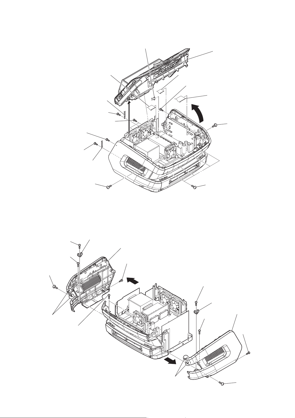
2-3. TOP PANEL SECTION
HCD-ZUX999
qg wire (flat type) (21 core)
(CN105)
4 screw
(+BVTP 3 u8)
3 screw
(+BVTP 3 u8)
1 screw
(+BVTP 3 u8)
8 screw
(case 3 TP2)
5 wire
6 two screws
(+BVTP 3 u8)
2 wire
qf CN107 (10P)
qh top panel section
qd wire (flat type) (31 core)
(CN101)
7 screw
(+BVTP 3 u8)
qs wire (flat type) (31 core)
(CN118)
qa
9 screw
(case 3 TP2)
0 four screws
(case 3 TP2)
2-4. SIDE PANEL (L) ASSY, SIDE PANEL (R) ASSY
5 screw
(+BVTP 3 u8)
4 screw
(+BVTP 3 u8)
2 screw
(case 3 TP2)
7 two claws
6 holder (side-support)
9 side panel (L) assy
3 screw
(+BVTP 3 u8)
8
1 two screws
(+BVTP 3 u8)
qd screw
(+BVTP 3 u8)
qf holder (side-support)
qj side panel (R) assy
qs screw
(+BVTP 3 u8)
qa screw
(+BVTP 3 u8)
qh
qg two claws
0 screw
(case 3 TP2)
11
HCD-ZUX999
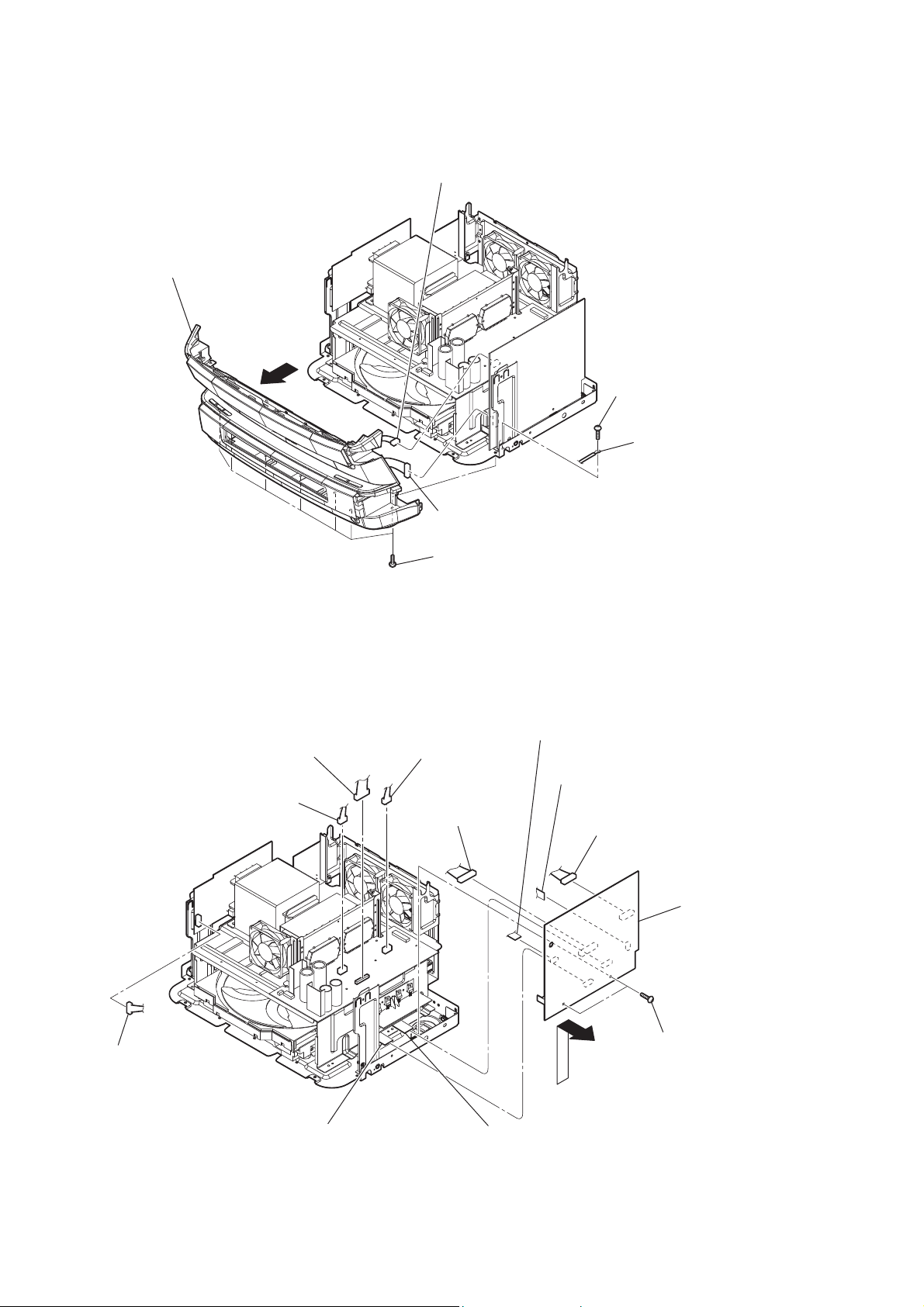
2-5. FRONT PANEL SECTION
7 front panel section
6
1 CN120 (6P)
3 screw
(+BVTP 3 u8)
4 wire
2-6. MAIN BOARD
3 CN857 (15P)
2 CN856 (4P)
2 CN115 (11P)
5 seven screws
(+BVTP 3 u8)
4 CN855 (5P)
6 CN111 (12P)
9 wire (flat type) (9 core)
(CN113 )
8 wire (flat type) (9 core)
(CN104)
7 CN103 (11P)
qd MAIN board
12
1 CN823 (7P)
qa wire (flat type) (13 core)
(CN109 )
0
qs wire (flat type) (19 core)
(CN106 )
5 two screws
(+BVTP 3 u8)
2-7. CD MECHANISM DECK
4 CD mechanism deck
3
2 two screws
(+BVTP 3 u8)
HCD-ZUX999
1 two screws
(+BVTP 3 u8)
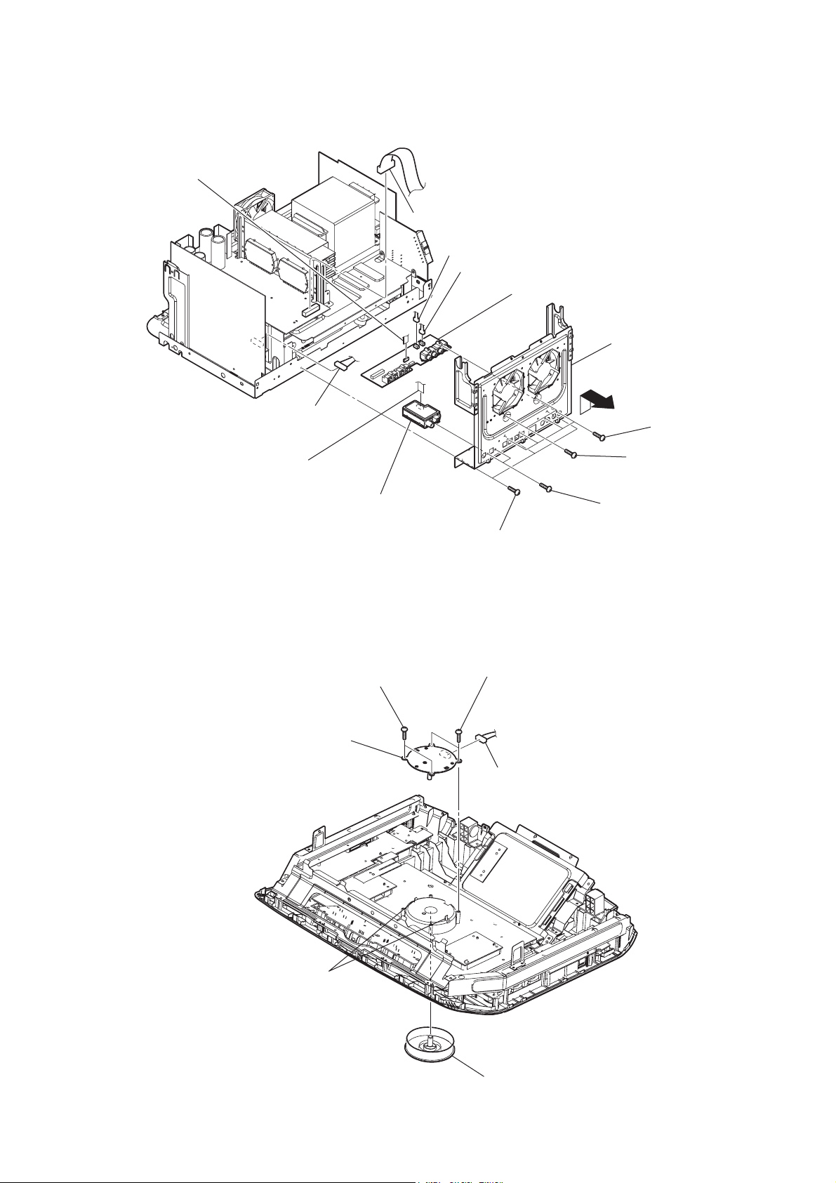
2-8. REGULATOR BOARD
2 REGULATOR board
1 three screws
(+BVTP 3 u8)
13
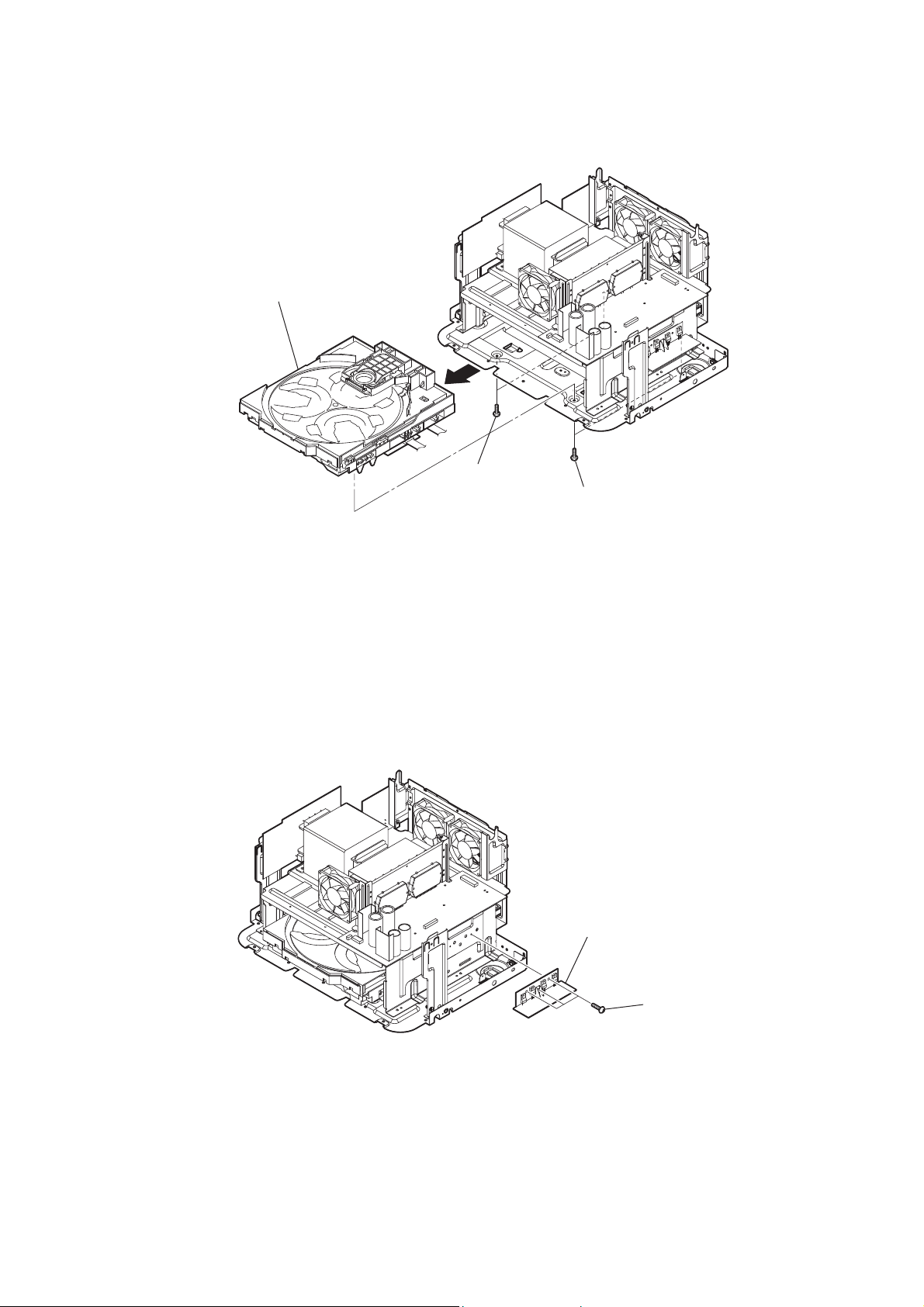
HCD-ZUX999
2-9. PT BOARD, SUB PT BOARD
7 CN824 (5P)
2 CN805 (6P)
5 two screws
(+BVTP 3 u8)
3 CN803 (3P)
1 CN801 (3P)
6 SUB PT board
4 two screws
(+BVTP 3 u8)
8 CN823 (7P)
9 two screws
qa PT board
0 two screws
2-10. AMP BOARD, DC FAN (FAN903)
qg heat sink
qh two screws
8 two screws
(+BVTP 3 u8)
qj DC fan (FAN903)
(+BVTP 3 u8)
qf two screws
(+BVTP 3 u8)
qk bracket (heatsink) (R)
qa two screws
(+BVTP 3 u8)
6 CN116 (3P)
9 two screws
(+BVTP 3 u8)
5 CN856 (4P)
4 CN857 (15P)
3 CN855 (5P)
2 CN854 (9P)
7 four screws
(+BVTP 3 u8)
qd AMP board
0
qs four screws
(transister)
14
1 CN824 (5P)
2-11. SPEAKER TERMINAL BOARD
8 wire (flat type) (9 core)
(CN004)
HCD-ZUX999
1 CN854 (9P)
7 CN006 (3P)
6 CN002 (3P)
0 SPEAKER TERMINAL board
back panel assy
2 CN103 (11P)
qa wire (flat type) (9 core)
2-12. X-ROUND JOG BOARD
5 X-ROUND JOG board
qd tuner (TU901)
4 two screws
(+BVTP 2.6 (3CR))
5
9 four screws
(+BVTP 3 u8)
4 two screws
(+BVTP 3 u8)
qs two screws
(+BVTP 3 u8)
3 three screws
(+BVTP 3 u8)
3 two screws
(+BVTP 2.6 (3CR))
2 CN1301 (6P)
two claws
1 jog-dial-assy
15
HCD-ZUX999
2-13. RIGHT ENTER BOARD, LEFT ENTER BOARD
1 screw
(+BVTP 2.6 (3CR))
3 screw
(+BVTP 2.6 (3CR))
5 RIGHT ENTER board
4 CN1432 (5P)
2 MAIN TO PANEL FFC board
6 three screws
(+BVTP 2.6 (3CR))
7 CN1437 (5P)
8 LEFT ENTER board
2-14. SH-TAS BOARD
claw
qs two rivets
qd SH BOARD FFC board
qh two screws
(+BVTP 3 u8)
1 CN603 (5P)
2 CN602 (9P)
3 wire (flat type) (31 core)
(CN101)
8 screw
(+BVTP 2.6 (3CR))
9 wiring stopper
0 screw
(+BVTP 2.6 (3CR))
claw
qa
qg two screws
(+BVTP 3 u8)
qj shield plate (SH-A)
qk four screws
(+BVTP 3 u8)
4 CN604 (5P)
6 wiring stopper
w; SH-TAS board
qf wire (flat type) (21 core)
(CN600)
5 screw
(+BVTP 2.6 (3CR))
ql shield plate (SH-B)
16
7 screw
(+BVTP 2.6 (3CR))
2-15. PANEL FUNCTION BOARD
HCD-ZUX999
qa wire (flat type) (13 core)
(CN1003)
6 CN1551 (3P)
CROSS FADER board
Tap the dial with a flathead screwdriver
or other tool harder to remove it.
flathead screwdriver
claw
claw
claw
claw
1 BTN-enter-B-assy
4 nine screws
(+BVTP 2.6 (3CR))
qs wire (flat type) (13 core)
(CN1012)
claw
3 two jog dial (enter)
claw
7 CN1010 (4P)
qd wire (flat type) (17 core)
(CN1001)
claw
2 BTN-enter-B-assy
8 wire (flat type) (13 core)
(CN1008)
5 nine screws
(+BVTP 2.6 (3CR))
9 CN1011 (4P)
qf PANEL FUNCTION board
0
claw
2-16. FL-TUBE BOARD, CROSS FADER BOARD
4 CROSS FADER board
7 screw
(+BVTP 2.6 (3CR))
1 four screws
(+BVTP 2.6 (3CR))
8 SIDE COVER R board
9 L-SHAPE ILLUMINATION-B board
3 two screws
(+B 3 u6)
2
5 four screws
(+BVTP 2.6 (3CR))
6 FL-TUBE board
0 screw
(+BVTP 2.6 (3CR))
qa SIDE COVER L board
qs L-SHAPE ILLUMINATION-A board
17
HCD-ZUX999
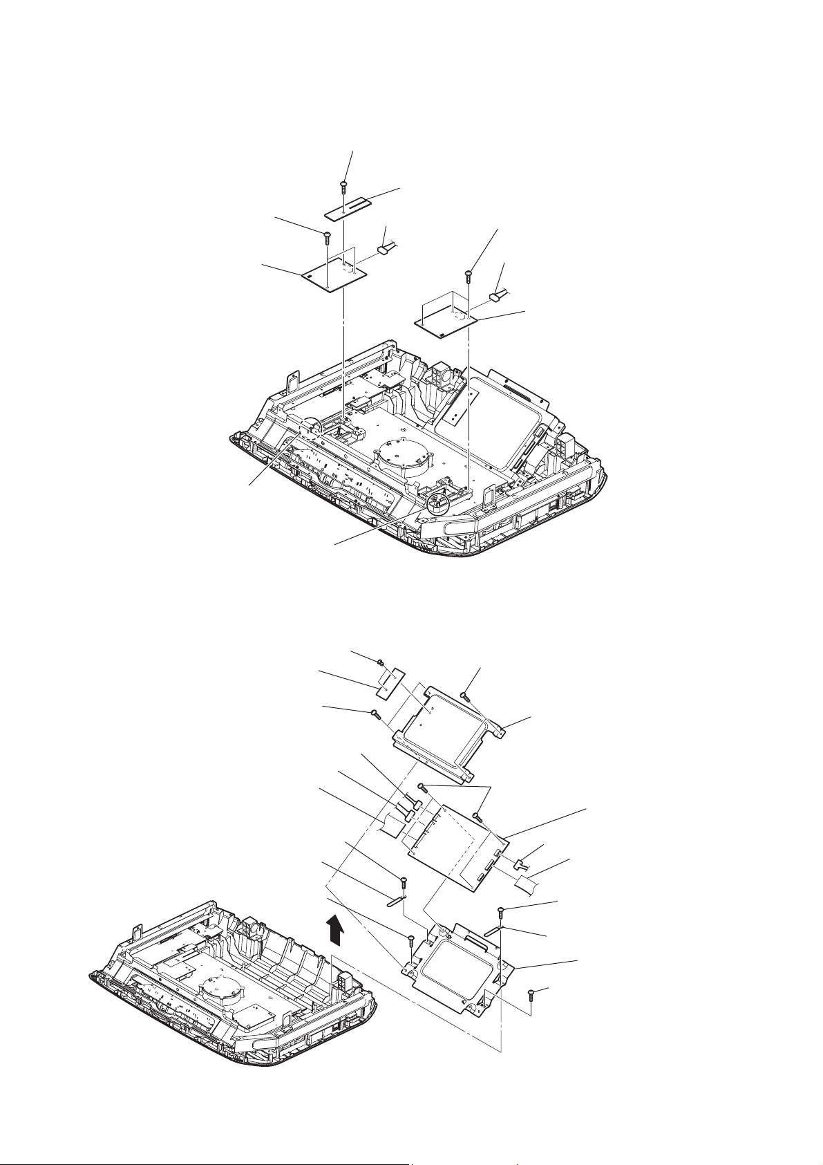
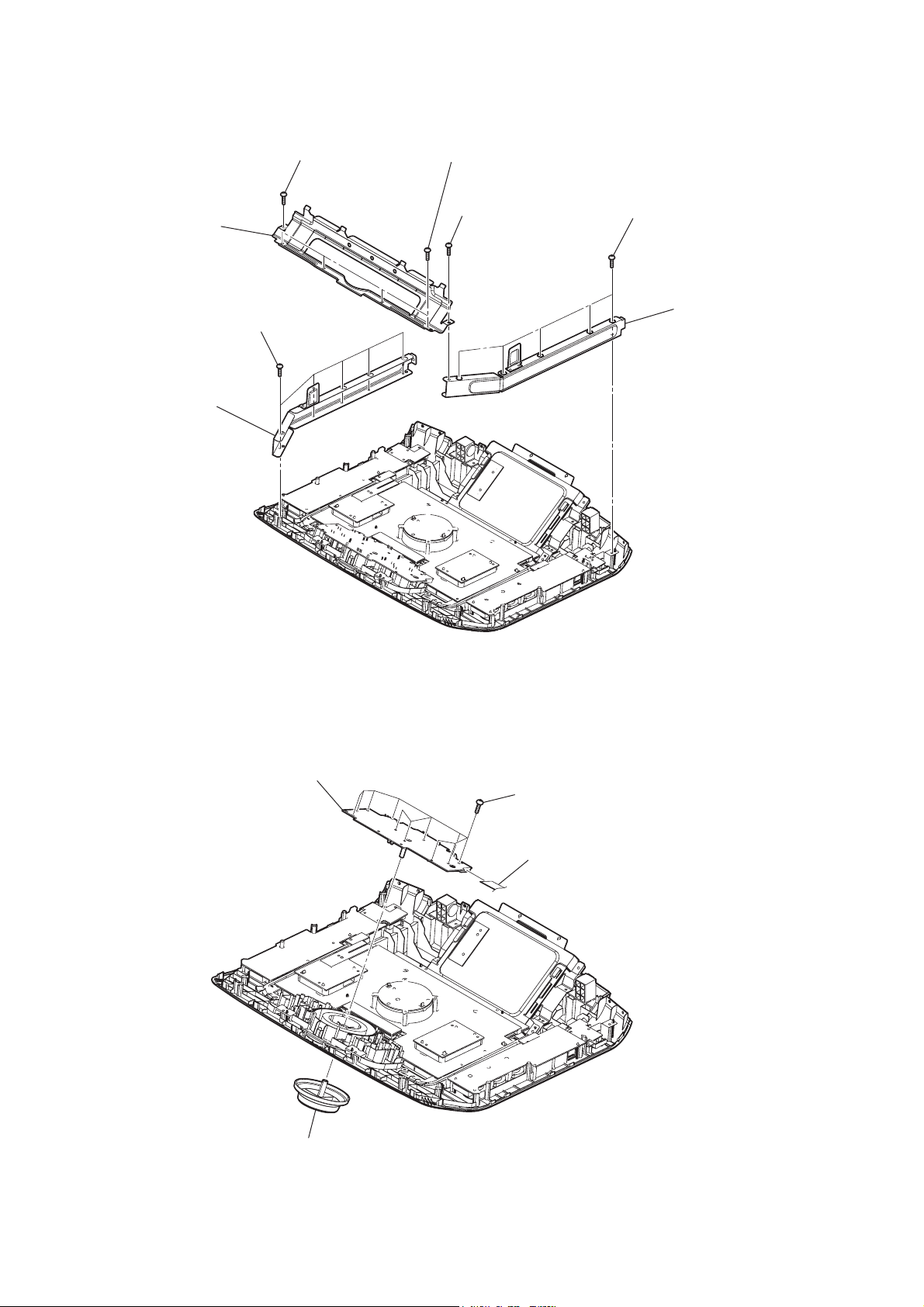
2-17. BRACKETS
4 bracket top (F)
5 five screws
(+BVTP 2.6 (3CR))
6 bracket top (R)
2 screw
(+BVTP 3 u8)
3 four screws
(+BVTP 2.6 (3CR))
1 screw
(+BVTP 3 u8)
7 five screws
(+BVTP 2.6 (3CR))
8 bracket top (L)
2-18. MASTER VOLUME BOARD
4 MASTER VOLUME board
3 eleven screws
(+BVTP 2.6 (3CR))
2 wire (flat type) (13 core)
(CN1393)
1 knob (VOL)
18
2-19. LEFT PANEL BOARD, USB-A BOARD
HCD-ZUX999
5 LEFT PANEL board
2 wire (flat type) (17 core)
(CN1304)
4 ten screws
(+BVTP 2.6 (3CR))
3 CN1307 (2P)
6 CN604 (5P)
7 three screws
(+BVTP 2.6 (3CR))
0 screw
(+BVTP 2.6 (3CR))
8 screw
(+BVTP 2.6 (3CR))
9 wire
qs ground (USB) (R) plate
qa USB-A board
1 three knobs (EQ)
2-20. RIGHT PANEL BOARD, USB-B BOARD
0 screw
(+BVTP 2.6 (3CR))
7 three screws
(+BVTP 2.6 (3CR))
qa USB-B board
4 ten screws
(+BVTP 2.6 (3CR))
5 RIGHT PANEL board
2 wire (flat type) (13 core)
(CN1362)
3 CN1364 (3P)
8 screw
(+BVTP 2.6 (3CR))
9 wire
qs ground (USB) (R) plate
6 CN603 (5P)
1 two knobs (MIC)
19
HCD-ZUX999
2-21. BOTTOM SIRCS BOARD, OPEN/CLOSE KEY BOARD, DISC FUNCTION BOARD
2 plate (screw)
claw
9 button (eject)
1 screw
(+BVTP 2.6 (3CR))
3 two screws
(+BVTP 2.6 (3CR))
4 BOTTOM SIRCS board
6 four screws
(+BVTP 2.6 (3CR))
claw
8 OPEN/CLOSE KEY board
5 CN1429 (3P)
7 four screws
(+BVTP 2.6 (3CR))
claw
qg button (disc)
qs four screws
(+BVTP 2.6 (3CR))
claw
qf DISC FUNCTION board
qd four screws
(+BVTP 2.6 (3CR))
qa plate (screw)
0 screw
(+BVTP 2.6 (3CR))
2-22. MICROPHONE BOARD, HEADPHONE BOARD
2 two screws
(+BVTP 3 u8)
4 bracket (MIC)
8 bracket (HP)
3 MICROPHONE board
6 two screws
(+BVTP 3 u8)
7 HEADPHONE board
5 four screws
(+BVTP 2.6 (3CR))
20
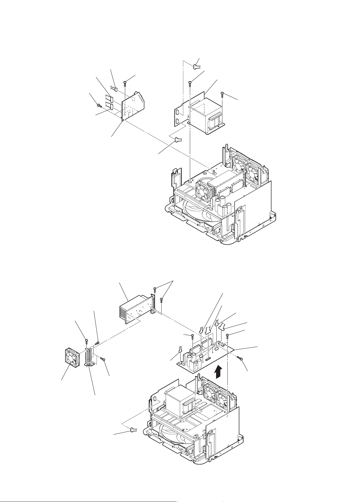
1 four screws
(+BVTP 2.6 (3CR))

2-23. BASE UNIT
HCD-ZUX999
5 wire (flat type) (19 core)
(CN101)
6 base unit
2-24. BD BOARD
4 two floating
(+PTPWH M2.6)
screws
5 optical pick-up
3 two floating
(+PTPWH M2.6)
1 two screws
(+BVTP 3 u8)
screws
2 lid (BU)
2 Remove the two solders.
1 wire (flat type)(16 core)
(CN301)
4 BD board
3 Remove the two solders.
21
HCD-ZUX999
2-25. DRIVER BOARD, SW BOARD
2 SW board
7 wire (flat type) (5 core)
(CN702)
4 CN703 (4P)
6 DRIVER board
2-26. SENSOR BOARD
2
tray
1
screw
(+BTTP (M2.6))
1 floating
(+PTPWH M2.6)
6 floating
(+PTPWH M2.6)
7
gear (geneva)
screw
8
screw
(+BTTP (M2.6))
screw
3 CN704 (2P)
9
SENSOR board
0
CN731
(3P)
5 two
screws
(+BTTP (M2.6))
3
belt (table)
4 floating
(+PTPWH M2.6)
5
pulley (table)
screw
22
2-27. MOTOR (TB) BOARD
table assy
2
stopper
1
2
stopper
6
table motor assy (M741)
HCD-ZUX999
2-28. MOTOR (LD) BOARD
4
Remove the two solders of motor.
5
loading motor assy (M751)
4
MOTOR (TB) board
5
Remove the two solders of motor.
3 two
screws
(+BTTP (M2.6))
2 two
screws
(+BTTP (M2.6))
3
MOTOR (LD) board
1
belt (loading)
23

HCD-ZUX999
SECTION 3
TEST MODE
[COLD RESET]
The cold reset clears all data including preset data stored in the
RAM to initial conditions. Execute this mode when returning the
set to the customer.
Procedure:
1. Press [
2. Press [x] button at channel A, [ENTER] button at channel B,
and [
3. “COLD RESET” appears on the fl uorescent indicator tube.
After that, the fl uorescent indicator tube becomes blank for a
while, and the system is reset.
[MC TEST MODE]
This mode is used to check operations of the respective sections of
Amplifi er and Tape.
Note: When VOLUME MAX is selected during MC TEST MODE, a con-
Procedure:
• To enter MC Test Mode
1. Press [x] button at channel A, [ENTER] button at channel B
and [X-MAXIMIZER] button simultaneously.
2. The line image display fl ashes on the fl uorescent indicator
tube. The function is no changed. The volume is changed to
VOLUME MIN/MAX.
• Check of Amplifi er
1. Turn [HIGH] or [MID] or [LOW] dial repeatedly until a message “GEQ MAX” appears on the fl uorescent indicator tube.
GEQ increases to its maximum.
2. Turn [HIGH] or [MID] or [LOW] dial repeatedly until a message “GEQ MIN” appears on the fl uorescent indicator tube.
GEQ decreases to its minimum.
3. Turn [HIGH] or [MID] or [LOW] dial repeatedly until a message “GEQ FLAT” appears on the fl uorescent indicator tube.
GEQ is set to fl at.
4. When the [MASTER VOLUME] knob is turned clockwise
even slightly, the sound volume increases to its maximum and
a message “VOLUME MAX” appears on the fl uorescent indi-
cator tube.
5. When the [MASTER VOLUME] knob is turned counterclockwise even slightly, the sound volume decreases to its minimum
and a message “VOLUME MIN” appears on the fl uorescent
indicator tube.
6. Press [DJ MODE] button to enter the DJ MODE.
7. Use [CROSS FADER] to select FADER operation at channel
A and at channel B.
8. Use [i LEVEL] to check the headphone level.
9. Use [MIC LEVEL] to check the microphone level.
• To release from Common Test mode
1. To release from this mode, press [
2. The cold reset is enforced at the same time.
] button to turn on the system.
@/1
] button simultaneously.
@/1
siderable level of volume will be outputted from the speaker. Because of this, a resistor of several hundred ohms to several kilohms
in series should be connected for attenuation.
] button.
@/1
[PANEL TEST MODE]
This mode is used to check the software version, FL and KEY.
• Display Test Mode
Procedure:
1. Press the [
2. Press [x] button at channel A, [ENTER] button at channel B,
and [ILLUMINATION] button simultaneously.
3. All LEDs and segments in fl uorescent indicator tube are turned
on. “All LEDs are turned off.” should be removed.
4. To exit from this mode, press [x] button at channel A, [ENTER] button at channel B, and [ILLUMINATION] button simultaneously.
• Version Test Mode
Procedure:
1. When the display test mode is activated, press the [GROOVE]
button and the message “ZTX 4CH LAT” is displayed, the version test mode is activated.
2. Whenever the [GROOVE] button is pressed, the display
changes in the following order.
3. To exit from this mode, press [x] button at channel A, [ENTER] button at channel B, and [ILLUMINATION] button simultaneously.
• FL Pattern Test Mode
Procedure:
1. When the display test mode is activated, press the [LEVEL
INDICATOR] button to select the FL pattern test mode.
2. When in the FL pattern test mode, half segments of fl uorescent
indicator tube and half lamps are turned on.
3. Press the [LEVEL INDICATOR] button. The remaining half
segments of the fl uorescent indicator tube and the remaining
half lamps are turned on.
4. Next press the [LEVEL INDICATOR] button, all the segments
of the fl uorescent indicator tube are turned off.
5. To exit from this mode, press [x] button at channel A, [ENTER] button at channel B, and [ILLUMINATION] button simultaneously.
• Key Test Mode
Procedure:
1. When the display test mode is activated, press the [ILLUMINATION] button to select the key test mode.
J: Search dial at channel A or B
C: CROSS FADER
K: Keys
V: MASTER VOLUME
X: OPERATION JOG dial
MIC: MIC LEVEL dial
HP: HEADPHONE LEVEL dial
L: LOW dial
M: MID dial
H: HIGH dial
] button to turn the power on.
?/1
ZTX 4CH LAT t SC Version t GC Version t
t SYS Version t STLW Version t STLM Version t
t ST Version t TA Version t TM Version
Key Test Mode display
J0 K0 J0 MIC 0 HP 0
V0 C0 X0 L0 M9 H2
24

HCD-ZUX999
2. To enter the KEY test mode, the fl uorescent indicator tube dis-
plays “K0”. Each time an another button is pressed, “KEY”
value increases. However, once a button is pressed, it is no
longer taken into account. When all keys are pressed correctly,
“K62” is displayed.
3. When the [MASTER VOLUME] control is turned in the direction of (+), “V0” is changed to “V1”, then ... “V9”.
When the [MASTER VOLUME] control is turned in the direc-
tion of (–), “V0” is changed to “V9”, then ... “V1”.
4. Just like the [MASTER VOLUME] control, by operating the
respective dials, their settings are changed as given below:
J: 0 to 9
C: 0 to 25
X: 0 to 9
L: 0 to 9
M: 0 to 9
H: 0 to 9
MIC: 0 to 19
HP: 0 to 31
5. To exit from this mode, disconnect the power cord to turn off
the system.
[CD SHIP MODE (WITHOUT MEMORY CLEAR)]
This mode moves the optical pick-up to the position durable to
vibration. Use this mode when returning the set to the customer
after repair.
Procedure:
1. Press [
] button to turn on the system.
@/1
2. Select CD function without disc.
3. Press [CD/DISC] button and [
] button simultaneously. The
@/1
system turns off automatically.
4. After the “STANDBY” blinking display fi nishes, a message
“MECHA LOCK” is displayed on the fl uorescent indicator
tube and the CD ship mode is set.
5. To exit from this mode, disconnect the power cord to turn off
the system.
[CD SHIP MODE (WITH MEMORY CLEAR)]
This mode moves the optical pick-up to the position durable to vibration and clears all data including preset data stored in the RAM
to initial conditions during the next AC-In. Use this mode when
returning the set to the customer after repair.
Procedure:
1. Press [
] button to turn on the system.
@/1
2. Select CD function.
3. Press [x] button at channel B, [CD/DISC] button and [
@/1
button simultaneously. The system turns off automatically.
4. After the “STANDBY” blinking display fi nishes, a message
“MECHA LOCK” is displayed on the fl uorescent indicator
tube and the CD ship mode is set.
5. To exit from this mode, disconnect the power cord to turn off
the system.
[DISC THEFT PREVENTION MODE]
The disc tray lock function for the antitheft of an demonstration
disc in the store is equipped.
Setting Procedure:
1. Press the [
] button to turn the set on.
?/1
2. Press the [CD/DISC] button to set CD function.
3. Insert a disc.
4. Press the [x] button at channel A and the [Z OPEN/CLOSE]
button simultaneously for fi ve seconds.
5. The message “LOCKED” is displayed and the tray is locked.
Releasing Procedure:
1. Press the [x] button at channel A and the [Z OPEN/CLOSE]
button simultaneously for fi ve seconds again.
2. The message “UNLOCKED” is displayed and the tray is unlocked.
Note: When “LOCKED” is displayed, the tray lock is not released by
turning power on/off with the [?/1] button.
[TUNER STEP CHANGE]
The step interval of AM channels can be toggled between 9 kHz
and 10 kHz. This mode is not available for Saudi Arabian and Russian models.
Procedure:
1. Press [
] button to turn on the system.
?/1
2. Press [TUNER/BAND] button repeatedly to select the “AM”.
3. Press [
4. Press [ENTER] button at channel A and [
] button to turn off the system.
?/1
] button simulta-
?/1
neously. The system turns on automatically. The message “AM
9K STEP” or “AM 10K STEP” appears on the fl uorescent in-
dicator tube and thus the channel step is changed.
[VACS ON/OFF]
This mode is used to switch ON and OFF the VACS (Variable Attenuation Control System).
Procedure:
1. Press [
] button to turn on the system.
@/1
2. Press [x] button at channel A and [OPTIONS] button simultaneously. The message “VACS OFF” or “VACS ON” appears
on the fl uorescent indicator tube.
[VACS DISPLAY]
This mode is used to check the VACS level.
Procedure:
1. Press [
] button to turn on the system.
@/1
2. Press [x] button at channel A, [CD/DISC] button and [RE-
]
TURN] button at channel B simultaneously.
3. The fl uorescent indicator tube displays “VACS$ AP#”.
“VACS” represents Conventional VACS (Triggered by signal
level)
“AP” represents APVACS (Abuse Protection VACS)
“$” is the Conventional VACS level.
“#” is the APVACS level.
4. To exit from this mode, press [x] button at channel A, [CD/
DISC] button and [RETURN] button at channel B simultaneously.
25
HCD-ZUX999
[BPM RESET]
Procedure:
1. Press the [
] button to turn the power on.
?/1
2. Press [BEAT SPEED] button and [ENTER] button at channel
A simultaneously.
3. When this button is operated, display as “BPM RESET” for a
while and all of the settings are reset.
[CHAIN, CHAIN B, CHAIN C, CHAIN D]
Procedure:
1. Press the [
] button to turn the power on.
?/1
• CHAIN mode
2. Press [PAD 1] button and [PAD 2] button simultaneously.
3. The message “CHAIN 1 < – > 2” will be displayed on the
fl uorescent indicator tube.
4. The beats and the rhythm are changed by turning the [OPERATION JOG] dial clockwise and counterclockwise.
• CHAIN B mode
5. Press [PAD 3] button and [PAD 4] button simultaneously.
6. The message “CHAIN 3 < – > 4” will be displayed on the
fl uorescent indicator tube.
7. The beats and the rhythm are changed by turning the [OPERATION JOG] dial clockwise and counterclockwise.
• CHAIN C mode
8. Press [PAD 1] button and [PAD 4] button simultaneously.
9. The message “CHAIN 1 < – > 4” will be displayed on the
fl uorescent indicator tube.
10. The beats and the rhythm are changed by turning the [OPERATION JOG] dial clockwise and counterclockwise.
• CHAIN D mode
11. Press [PAD 3] button and [PAD 2] button simultaneously.
12. The message “CHAIN 3 < – > 2” will be displayed on the
fl uorescent indicator tube.
13. The beats and the rhythm are changed by turning the [OPERATION JOG] dial clockwise and counterclockwise.
[X-TRANCE DEMO MODE]
Procedure:
1. Press [
] button to turn on the system.
?/1
2. Press [ENTER] button at channel A and [BEAT PATTERN]
button simultaneously.
3. The message “X-TRANCE PRO DEMO” will be displayed on
the fl uorescent indicator tube.
4. The Demo mode is entered.
5. To exit from this mode, press any button on the panel. “DEMO
OFF” will be displayed, exiting from the Demo mode.
[BD FACTORY MODE]
Procedure:
1. Press [
] button to turn on the system.
@/1
2. Select CD function.
3. Press [x] button at channel A, [MP3 BOOSTER] button and
[RETURN] button at channel B simultaneously.
4. “FACTORY MODE” will be displayed for a moment, entering
the mode.
• AGC mode
5. The AGC value is indicated each time the [i CUE A] button is
pressed.
“TRK_AG XX”
“––x1ON”
“FCS–AG XX”
XX: AGC value
• RF GAIN mode
6. The RF GAIN value is indicated each time the [BEAT SPEED]
button is pressed.
“ALx YYN”
“RWx YYN”
“––x1ON”
YY: GAIN value
• TRK ON/OFF
7. TRK is switched between TRK ON and OFF each time the
[AUDIO IN 2] button.
“––x1ON” “––x1OFF”
• PLAYING SPEED mode
8. The CD playing speed is changed as given below each time the
[SURROUND] button is pressed.
“––x1OFF”
“––x2OFF”
“––x4OFF”
• S-CURVE ON/OFF mode
9. S-CURVE is switched between S-CURVE ON and OFF each
time the [GROOVE] button is pressed.
“––x1OFF” “––x1OFF SCURVE”
26
Set value of the PLAYING SPEED
• LAST TrK + PLAY mode
10. The last track of the CD disk is played back by pressing the
[RETURN] button at channel A. However, the items 7, 8 and 9
must be at their normal settings.
• To exit from this mode
11. Press [x] button at channel A, [MP3 BOOSTER] button and
[RETURN] button at channel B simultaneously.
SECTION 4
ELECTRICAL CHECKS
HCD-ZUX999
CD SECTION
Note:
1. CD Block is basically designed to operate without adjustment. Therefore, check each item in order given.
2. Use YEDS-18 disc (3-702-101-01) unless otherwise indicated.
3. Use an oscilloscope with more than 10 MΩ impedance.
4. Clean the object lens by an applicator with neutral detergent when the
signal level is low than specifi ed value with the following checks.
RF LEVEL CHECK
oscilloscope
CD board
TP216 (RFACO)
TP5 (VC)
Procedure:
1. Connect an oscilloscope TP216 (RFACO) and TP5 (VC) on
the CD board.
2. Turn the power ON.
3. Load a disc (YEDS-18) and playback.
4. Confi rm that oscilloscope waveform is clear and check if RF
signal level is correct or not.
Note: Clear RF signal waveform means that the shape “ ◊ ” can be clearly
distinguished at the center of the waveform.
RF signal waveform
VOLT/DIV: 200 mV
TIME/DIV: 500 ns
level: 1.1 ± 0.3 Vp-p
Connecting and Adjustment Location: CD board
– CD BOARD (CONDUCTOR SIDE) –
TP5
(VC)
TP3
(TEI)
TP216
(RFACO)
TUNER SECTION
FM TUNE LEVEL CHECK
signal
generator
Procedure:
1. Turn on the set.
2. Input the following signal from signal generator to FM antenna
input directly.
set
E-F BALANCE (1 TRACK JUMP) CHECK
oscilloscope
CD board
TP3 (TEI)
TP5 (VC)
Procedure:
1. Connect an oscilloscope to TP3 (TEI) and TP5 (VC).
2. Turn the power ON.
3. Load a disc (YEDS-18) and playback the number 5 track.
4. Confi rm that the level B and A (DC voltage) on the oscillo-
scope waveform.
1 track jump waveform
DVC
level = 1.3 ± 0.6 Vp-p
B
symmetry
center of
waveform
A (DC voltage)
Carrier frequency : A = 87.5 MHz, B = 98 MHz, C = 108 MHz
Deviation : 75 kHz
Modulation : 1 kHz
ANT input : 35 dBu (EMF)
Note: Use 75 ohm coaxial cable to connect signal generator and the set.
You cannot use video cable for checking.
Use signal generator whose output impedance is 75 ohm.
3. Set to FM tuner function and tune A, B and C signals.
4. Confi rm “TUNED” is lit on the display for A, B and C signals.
When the selected station signal is received in good condition,
“TUNED” is displayed.
27

HCD-ZUX999
MEMO
28
SECTION 5
DIAGRAMS
HCD-ZUX999
• Circuit Boards Location
L-SHAPE ILLUMINATION-A board
LEFT PANEL board
PANEL FUNCTION board
LEFT ENTER board
MASTER VOLUME board
DISC FUNCTION board
HEADPHONE board
CROSS FADER board
RIGHT ENTER board
PT board
USB-A board
SUB PT board
FL-TUBE board
SH-TAS board
MICROPHONE board
SENSOR board
L-SHAPE ILLUMINATION-B board
USB-B board
X-ROUND JOG board
RIGHT PANEL board
BOTTOM SIRCS board
OPEN/CLOSE KEY board
SPEAKER TERMINAL board
AMP board
THIS NOTE IS COMMON FOR PRINTED WIRING BOARDS AND SCHEMATIC DIAGRAMS.
(In addition to this, the necessary note is printed in each block.)
For Printed Wiring Boards.
Note:
• X : Parts extracted from the component side.
• Y : Parts extracted from the conductor side.
• : Pattern from the side which enables seeing.
(The other layers’ patterns are not indicated.)
Caution:
Pattern face side:
(Conductor Side)
Parts face side:
(Component Side)
• Indication of transistor.
Q
B
E
Q
G
S
Q
B
CE
• Abbreviation
E2 : 120V AC area in E model
E3 : 240V AC area in E model
E51 : Chilean and Peruvian models
MX : Mexican model
Parts on the pattern face side seen
from the pattern face are indicated.
Parts on the parts face side seen from
the parts face are indicated.
These are omitted.
These are omitted.
These are omitted.
UNLEADED SOLDER
Boards requiring use of unleaded solder are printed with the leadfree mark (LF) indicating the solder contains no lead.
(Caution: Some printed circuit boards may not come printed with
the lead free mark due to their particular size)
For Schematic Diagrams.
Note:
• All capacitors are in μF unless otherwise noted. (p: pF) 50
WV or less are not indicated except for electrolytics and
tantalums.
• All resistors are in Ω and 1/4 W or less unless otherwise
specifi ed.
• 2 : Nonfl ammable resistor.
• C : Panel designation.
Note: The components identifi ed by mark 0 or dotted
line with mark 0 are critical for safety.
Replace only with part number specifi ed.
• A : B+ Line.
• B : B– Line.
• Voltages and waveforms are dc with respect to ground
under no-signal (detuned) conditions.
no mark : TUNER
< > : CD PLAY
* : Impossible to measure
• Voltages are taken with VOM (Input impedance 10 MΩ).
Voltage variations may be noted due to normal production
tolerances.
• Waveforms are taken with a oscilloscope.
Voltage variations may be noted due to normal production
tolerances.
• Circled numbers refer to waveforms.
• Signal path.
F : TUNER (ANALOG)
L : TUNER (DIGITAL)
J : CD PLAY (ANALOG)
c : CD PLAY (DIGITAL)
N : MIC
• Abbreviation
E2 : 120V AC area in E model
E3 : 240V AC area in E model
E51 : Chilean and Peruvian models
MX : Mexican model
HCD-ZUX999
SW board
MOTOR (LD) board
MOTOR (TB) board
DRIVER board
MAIN board
BD board
REGULATOR board
: LEAD FREE MARK
Unleaded solder has the following characteristics.
• Unleaded solder melts at a temperature about 40 °C higher
than ordinary solder.
Ordinary soldering irons can be used but the iron tip has to be
applied to the solder joint for a slightly longer time.
Soldering irons using a temperature regulator should be set to
about 350 °C.
Caution: The printed pattern (copper foil) may peel away if
the heated tip is applied for too long, so be careful!
• Strong viscosity
Unleaded solder is more viscous (sticky, less prone to fl ow)
than ordinary solder so use caution not to let solder bridges
occur such as on IC pins, etc.
• Usable with ordinary solder
It is best to use only unleaded solder but unleaded solder may
also be added to ordinary solder.
2929
HCD-ZUX999
5-1. BLOCK DIAGRAM – CD SERVO Section –
OPTICAL PICK-UP
BLOCK
(KSM215DHAP)
VR
FOCUS
COIL
TRACKING
COIL
M401
(SPINDLE)
M402
(SLED)
VC
B
C
D
E
LD
GND
PD
F–
T–
T+
DIGITAL SERVO, DIGITAL SIGNAL PROCESSOR, D/A CONVERTER
25
A
F
VC
F+
+
–
+
–
CD A +3.3V
26
27
28
29
19
20
LD DRIVER
Q321
SPINDLE/SLED MOTOR DRIVER,
FOCUS/TRACKING COIL DRIVER
52
47
56
55
10
M
5
2
M
1
VO1+
VO1–
VO2+
VO2–
VO4+
VO4–
VO3+
VO3–
IC401
VREF
IN1+
IN1–
IN2+
IN2–
IN3+
IN3–
IN4
STBY
SW
22
35
34
32
31
27
26
23
8
19
36
37
25
13
14
11
12
9
10
6
VC
A
B
C
D
E
F
LD
PD
VC
FFDR
FRDR
TFDR
TRDR
SFDR
SRDR
MDP
IC201
AOUT1
AOUT2
DOUT
CLOK
SCOR
SENS
SSTP
XTAI
XTAO
XRST
XTACN
81
86
71
102DATA
105
104XLAT
115
107
7
78
77
100
95
R-CH
S201
(LIMIT IN)
X201
67.7376MHz
A
AUDIO
SECTION
CD-L
(Page 31)
DOUT
CD-RST
DSP
IC605 (1/3)
69
CD_DATA
62
CD_CLK
66
CD_XLAT
64
CD_SCOR
68
CD_SENS
81
TXD3
73
RXD3
82
CTS3
CDX-T-TACN
71
D441D440
CD-GAINSW
70
B
(Page 32)
USB
SECTION
SYSTEM CONTROL
IC111 (1/6)
STALLIO_TXD_OUT
35
STALLIO_RXD_IN
36
STALLIO_RTS
38 3
TBL-SENSE
CDM ENCODER SW0
CDM ENCODER SW1
CDM ENCODER SW2
LM-F
LMR
TM-F
TM-R
2
48
3
45
47
81
80
79
Q731
LD MOTOR DRIVER
FIN
7
RIN
9
TBL MOTOR DRIVER
FIN
7
RIN
9
TABLE ADDRESS SENSOR
IC731
4
IC701
DRIVE
IC712
DRIVE
OUT2
OUT1
OUT2
OUT1
RE701
ROTARY ENCODER
DISC TRAY
ADDRESS DETECT
MOTOR
MOTOR
MM
MM
M+9V
M751
(LOADING)
M741
(TABLE)
2
1
2
4
2
4
HCD-ZUX999
x R-ch is omitted due to same as L-ch.
x SIGNAL PATH
: CD PLAY (ANALOG)
: CD PLAY (DIGITAL)
OPEN-SW
21
S751
OPEN/CLOSE
DETECT
3030
 Loading...