


HCD-V909AV
SERVICE MANUAL
E Model
Chinese Model
HCD-V909AV is the tuner, deck, Video CD and amplifier section in MHC-V909AV.
|
|
Model Name Using Similar Mechanism |
HCD-V800 |
CD |
|
|
|
CD Mechanism Type |
CDM38L-5BD21AL |
||
SECTION |
|
|
|
Base Unit Type |
BU-5BD21AL |
||
|
|
|
|
|
|
Optical Pick-up Type |
KSS-213D/Q-NP |
|
|
|
|
TAPE |
Model Name Using Similar Mechanism |
HCD-V800 |
|
DECK |
|
|
|
|
Tape Transport Mechanism Type |
TCM-220WR2 |
|
SECTION |
|||
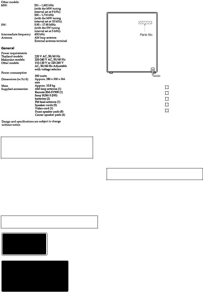
SPECIFICATIONS
— Continued on next page —
COMPACT DISC DECK RECEIVER
MICROFILM
— 1 —
CAUTION
Use of controls or adjustments or performance of procedures other than those specified herein may result in hazardous radiation exposure.
Notes on chip component replacement
•Never reuse a disconnected chip component.
•Notice that the minus side of a tantalum capacitor may be damaged by heat.
Flexible Circuit Board Repairing
•Keep the temperature of soldering iron around 270˚C during repairing.
•Do not touch the soldering iron on the same conductor of the circuit board (within 3 times).
•Be careful not to apply force on the conductor when soldering or unsoldering.
Laser component in this product is capable of emitting radiation exceeding the limit for Class 1.
This appliance is classified as a CLASS 1 LASER product. The CLASS 1 LASER PRODUCT MARKING is located on the rear exterior.
This caution label is located inside the unit.
MODEL IDENTIFICATION
— BACK PANEL — |
• Abbreviation |
|
|
SP |
: Singapore model |
|
MY : Malaysia model |
|
|
IA |
: Indonesian model |
|
CH |
: Chinese model |
|
TH |
: Thai model |
MODEL |
PARTS No. |
|
|
MY model |
4-991-746-4 |
|
|
TH model |
4-991-746-9 |
|
|
E, SP model |
4-991-753-0 |
|
|
CH model |
4-991-753-1 |
|
|
IA model |
4-991-753-2 |
|
|
SAFETY-RELATED COMPONENT WARNING !!
COMPONENTS IDENTIFIED BY MARK !OR DOTTED LINE WITH MARK !ON THE SCHEMATIC DIAGRAMS AND IN
THE PARTS LIST ARE CRITICAL TO SAFE OPERATION. REPLACE THESE COMPONENTS WITH SONY PARTS WHOSE PART NUMBERS APPEAR AS SHOWN IN THIS MANUAL OR IN SUPPLEMENTS PUBLISHED BY SONY.
NOTES ON HANDLINGTHE OPTICAL PICK-UP BLOCK OR BASE UNIT
The laser diode in the optical pick-up block may suffer electrostatic break-down because of the potential difference generated by the charged electrostatic load, etc. on clothing and the human body.
During repair, pay attention to electrostatic break-down and also use the procedure in the printed matter which is included in the repain parts.
The flexible board is easily damaged and should be handled with care.
NOTES ON LASER DIODE EMISSION CHECK
The laser beam on this model is concentrated so as to be focused on the disc reflective surface by the objective lens in the optical pickup block. Therefore, when checking the laser diode emission, observe from more than 30 cm away from the objective lens.
LASER DIODE AND FOCUS SEARCH OPERATION CHECK
Carry out the “S curve check” in “CD section adjustment” and check that the S curve waveform is output three times.
— 2 —
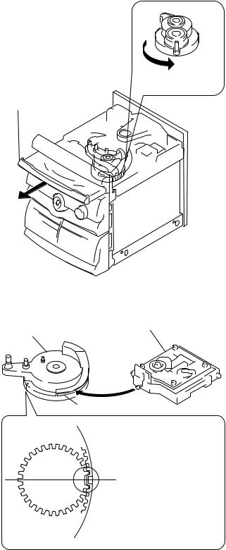
TABLE OF CONTENTS |
|
1. SERVICING NOTE .......................................................... |
3 |
2. GENERAL .......................................................................... |
6 |
3. DISASSEMBLY |
|
3-1. Back Panel ........................................................................... |
7 |
3-2. Loading Panel ....................................................................... |
8 |
3-3. CD Mechanism Deck ............................................................ |
8 |
3-4. Front Panel ........................................................................... |
9 |
3-5. TC Mechanism Deck and DECO Board ............................... |
9 |
3-6. HP/MIC Board, Display Board and TC SW Board ............ |
10 |
3-7. Disc Tray ........................................................................... |
10 |
4. TEST MODE .............................................................. |
11 |
5. MECHANICAL ADJUSTMENTS ........................... |
12 |
6. ELECTRICAL ADJUSTMENTS ............................... |
12 |
7. DIAGRAMS |
|
7-1. Circuit Boards Location ...................................................... |
17 |
7-2. Block Diagrams |
|
• KEY CON Section ........................................................... |
18 |
• CD Section ....................................................................... |
19 |
• Video Section ................................................................... |
21 |
• Deck Section .................................................................... |
23 |
• Main Section .................................................................... |
25 |
• Power Section .................................................................. |
27 |
7-3. Printed Wiring Board — CD Section — ............................. |
29 |
7-4. Schematic Diagram — CD Section — ............................... |
31 |
7-5. Schematic Diagram — Video Section — ........................... |
33 |
7-6. Printed Wiring Board — Video Section — ......................... |
37 |
7-7. Printed Wiring Board — Main Section — .......................... |
40 |
7-8. Schematic Diagram — Main Section — ............................ |
43 |
7-9. Schematic Diagram — Deck Section — ............................ |
47 |
7-10. Printed Wiring Board — Deck Section — ....................... |
51 |
7-11. Schematic Diagram — Panel Section — ......................... |
54 |
7-12. Printed Wiring Board — Panel Section — ....................... |
57 |
7-13. Schematic Diagram — Power Section — ........................ |
61 |
7-14. Printed Wiring Board — Power Section — ..................... |
65 |
7-15. Schematic Diagram — CD Motor Section — .................. |
68 |
7-16. Printed Wiring Board — CD Motor Section — ............... |
69 |
7-17. Schematic Diagram — KEY CON Section — ................. |
71 |
7-18. Printed Wiring Board — KEY CON Section — .............. |
72 |
7-19. IC Block Diagrams ........................................................... |
73 |
7-20. IC Pin Functions ............................................................... |
80 |
8. EXPLODED VIEWS |
|
8-1. Case Section ........................................................................ |
97 |
8-2. Main Board Section ............................................................ |
98 |
8-3. Panel Board Section ............................................................ |
99 |
8-4. Front Panel Section ........................................................... |
100 |
8-5. TC Mechanism Section 1 (TCM-220WR2) ...................... |
101 |
8-6. TC Mechanism Section 2 (TCM-220WR2) ...................... |
102 |
8-7. CD Mechanism Section 1 (CDM38L-5BD29AL) ............ |
103 |
8-8. CD Mechanism Section 2 (CDM38L-5BD29AL) ............ |
104 |
8-9. Base Unit Section (BU-5BD29AL) .................................. |
105 |
9. ELECTRICAL PARTS LIST ...................................... |
106 |
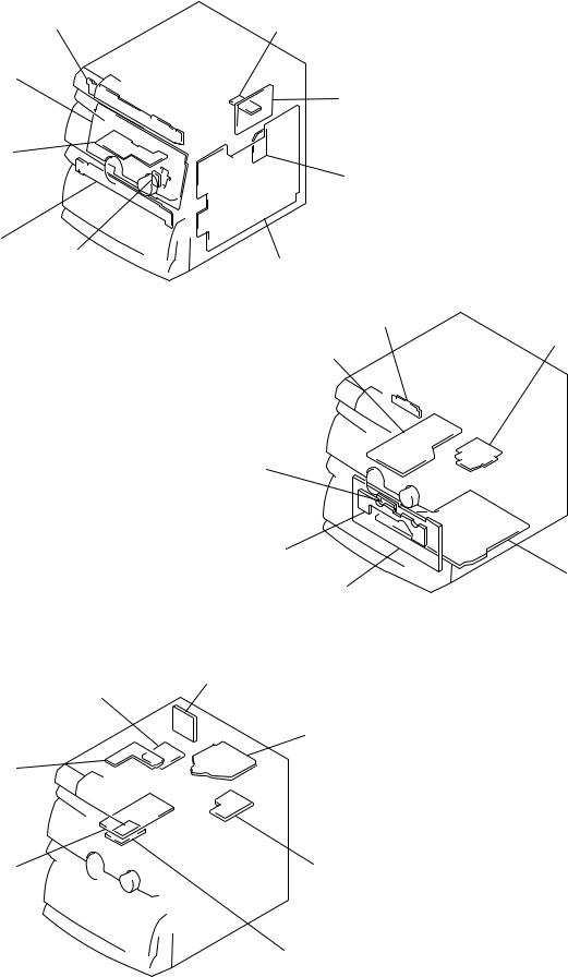
SECTION 1
SERVICING NOTE
HOW TO OPEN THE DISC TRAY WHEN POWER SWITCH TURNS OFF
1 Remove the Case.
2 Remove the Back panel.
3 Turn the cam to the direction of arrow.
4 Pull-out the disc tray.
Note for Installation (ROTARY ENCODER)
Note : When attaching the Base unit. insert the section A into the groove of BU cam.
BU cam
Section A
groove
Note : When attaching the BU cam, engage the Rotary encoder switch as shown in the figure.
— 3 —

MC Cold Reset
• The cold reset clears all data including preset data stored in the RAM to initial conditions. Execute this mode when returning the set to the customer.
Procedure:
1.Press three buttons NEXT , ENTER/NEXT , and DISC 1 simultaneously.
2.The fluorescent indicator tube becomes blank instantaneously, and the set is reset.
CD Delivery Mode
• This mode moves the pick-up to the position durable to vibration. Use this mode when returning the set to the customer after repair.
Procedure:
1.Press POWER button to turn the set ON.
2.Press PLAY MODE button and POWER button simultaneously.
3.A message “LOCK” is displayed on the fluorescent indicator tube, and the CD delivery mode is set.
MC Hot Reset
• This mode resets the set with the preset data kept stored in the memory. The hot reset mode functions same as if the power cord is plugged in and out.
Procedure:
1.Press three buttons NEXT , ENTER/NEXT , and DISC 2 simultaneously.
2.The fluorescent indicator tube becomes blank instantaneously, and the set is reset.
Sled Servo Mode
• This mode can run the CD sled motor freely. Use this mode, for instance, when cleaning the pick-up.
Procedure:
1. Select the function “CD”.
2. Press three buttons NEXT , ENTER/NEXT , and FUNC-
TION simultaneously.
3.The Sled Servo mode is selected, if “CD” is blanking on the fluorescent indicator tube.
4.With the CD in stop status, press ) button in CD section to move the pick-up to outside track, or 0 button to inside track.
5.To exit from this mode, perform as follows:
1)Move the pick-up to the most inside track.
2)Press three buttons in the same manner as step 2.
Note:
•Always move the pick-up to most inside track when exiting from this mode. Otherwise, a disc will not be unloaded.
•Do not run the sled motor excessively, otherwise the gear can be chipped.
Change-over of FUNCTION Name
• The FUNCTION name of external input terminal can be changed over to VIDEO or MD. With the FUNCTION selected to “MD”, about 5dB mute is applied to the input gain.
Procedure:
1.Press POWER button to turn the set OFF.
2.Press POWER button together with FUNCTION button, and the power is turned on, the display of fluorescent indicator tube changes to “MD” or “VIDEO” instantaneously, and thus the FUNCTION is changed over.
Change-over of AM Tuner Step between 9kHz and 10kHz
• A step of AM channels can be changed over between 9kHz and 10kHz.
Procedure:
1.Press POWER button to turn the set ON.
2.Select the function “TUNER”, and press TUNER/BAND button to select the BAND “AM” or “MW”.
3.Press POWER button to turn the set OFF.
4.Press ENTER/NEXT and POWER buttons simultaneously, and the display of fluorescent indicator tube changes to “9k STEP” or “10k STEP”, and thus the channel step is changed over.
LED and Fluorescent Indicator Tube All Lit, Key Check
Mode
Procedure:
1.Press three buttons NEXT , ENTER/NEXT , and DISC 3 simultaneously.
2.LEDs and fluorescent indicator tube are all turned on. Press DISC 2 button, and the key check mode is activated.
3.In the key check mode, the fluorescent indicator tube displays
“K 1 V0 J0”. Each time a button is pressed, “K”value increases. However, once a button is pressed, it is no longer taken into account.
“J” Value increases like 1, 2, 3 ... if rotating JOG knob in “+” direction, or it decreases like 0, 9, 8 ... if rotating in “–” direction.
“V” Value increases like 1, 2, 3 ... if rotating VOLUME knob in “+” direction, or it decreases like 0, 9, 8 ... if rotating in “–” direction.
4.To exit from this mode, press three buttons in the same manner as step 1, or disconnect the power cord.
Aging Mode
This mode can be used for operation check of CD section and tape deck section.
• If an error occurred:
The aging operation stops.
• If no error occurs:
The aging operation continues repeatedly.
1. Aging Mode in CD Section
1-1. Operating procedure of Aging Mode
1.Set discs in DISC 1 and DISC 2 trays.
2.Select the function “CD”.
3.Press three buttons NEXT , ENTER/NEXT , and KARAOKE PON/MPX simultaneously.
4.The aging mode is activated, if a roulette mark on the fluorescent indicator tube is blinking.
5.In the aging mode, the aging is executed in a sequence given in “1-2. Operation during Aging Mode”.
The aging continues unless an alarm occurred.
6.To exit from the aging mode, press POWER button to turn the set OFF.
∙If a button other than buttons In CD section is pressed during aging, the aging in the CD section is finished.
∙To execute aging to the tape deck section successively, press á button in the deck A.
“AGING” is displayed on the fluorescent indicator tube. (For the aging in tape deck, see “2. Aging Mode in Tape Deck Section”.
1-2. Operation during aging Mode
In the aging mode, the program is executed in the following sequence.
1.The disc table is ejected.
2.The disc tray turns to select a disc. (For a disc selection sequence, see Section 1-3.)
3.TOC of disc is read.
4.The pick-up accesses to the last track.
5.Disc table is ejected.
6.Steps 2 through 5 are repeated.
— 4 —
1-3. Disc Selection Sequence
∙During the aging mode, discs are selected in the following sequence:
Disc 1 → Disc 2
− ↓
Disc 2 ← Disc 1
2.Aging Mode in Tape Deck Section
2-1. Operating procedure of Aging Mode
1.Load a commercially available 10-minute tape into the decks A and B respectively.
(If a 10-minute tape is not available, another tape may be used but a cycle time will be longer.)
2.Select the function “TAPE”.
3.Rewind tapes in advance by pressing 0 button respectively on decks A and B.
4.Press three buttons NEXT , ENTER/NEXT , and KARAOKE PON/MPX simultaneously.
5.Press á button on deck A. (This button triggers the aging mode.)
6.The aging mode is activated if “AGING A” is displayed on the fluorescent indicator tube.
7.In the aging mode, the aging is executed in a sequence given in “2-2. Operation during Aging Mode”.
The aging continues unless an alarm occurred.
8.To exit from the aging mode, press POWER button to turn the set OFF.
2-2. Operation during Aging Mode
In the aging mode, the program is executed in the following sequence.
1.A tape on FWD side is played for one minute.
2.PAUSE STOP is made.
3.Recording is made for 3 minutes. (For the deck not having the record function, the play is executed. In this case, á LED does not light up.)
4.FF is executed up to the end of tape.
5.A tape is reversed, and the tape on REV side is played for one minute.
6.PAUSE STOP is made.
7.Recording is made for 3 minutes. (For the deck not having the record function, the play is executed. In this case, » LED does not light up.)
8.FF is executed up to the end of tape.
9.Steps 1 through 8 are executed for the other deck.
10.Steps 1 through 9 are repeated unless an alarm occurred.
2-3. Deck Selection Sequence
• During the aging mode, decks are selected in the following sequence:
Deck A (FWD) → Deck A (REV) − ↓
Deck B (REV) ← Deck B (FWD)
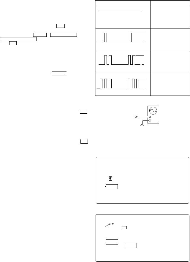
SELF-DIAGNOSIS
This model has the self-diagnosis function for the VIDEO and AUDIO decoder sections.
Immediately after the power on, the self-diagnosis function searches each operation of IC’s around the mechanism control microcomputer (IC701).
The results can be checked by connecting an oscilloscope to TP709 (LED) of theVIDEO board.
Oscilloscope (Waveform) |
Symptom |
H
No error
L
Light
H
External SRAM (IC751) L error
1 time blinking
H
MPEG decoder (IC201) L error
2 time blinking
H
DRAM (IC251) error
L
3 time blinking
oscilloscope
VIDEO board
TP709 (LED) +
–
Note: The LED for check (D701) is mounted to some sets (FORMER TYPE). In this case, confirm the lighting condition of LED.
[VIDEO BOARD] (SIDE A)
D701
IC771
[VIDEO BOARD] (SIDE B)
X901
TP709 (LED)
 IC751
IC751
IC251 
— 5 —
SECTION 2
GENERAL
Front Panel
1 |
2 |
3 |
4 |
5 |
6 |
7 |
8 |
9 |
10 11 |
12 |
13 14 |
15 |
16 |
17 |
18 |
19 |
20 |
|
21 |
||
50 |
|
|
|
|
|
|
|
|
|
|
|
|
|
|
49 |
|
|
|
|
|
|
|
|
|
|
|
|
|
22 |
|
|
|
|
|
|
|
|
|
|
|
|
|
|
|
48 |
|
|
|
|
|
|
|
|
|
|
|
|
|
|
47 |
|
|
|
|
|
|
|
|
|
|
|
|
|
|
46 |
|
|
|
|
|
|
|
|
|
|
|
|
|
|
45 |
|
|
|
|
|
|
|
|
|
|
|
|
|
|
44 |
|
|
|
|
|
|
|
|
|
|
|
|
|
23 |
43 |
|
|
|
|
|
|
|
|
|
|
|
|
|
|
42 |
|
|
|
|
|
|
|
|
|
|
|
|
|
24 |
|
|
|
|
|
|
|
|
|
|
|
|
|
|
|
41 |
|
|
|
|
|
|
|
|
|
|
|
|
|
|
40 |
|
|
|
|
|
|
|
|
|
|
|
|
|
|
39 |
38 |
37 |
36 |
35 |
34 |
33 |
32 |
31 |
30 |
29 28 |
27 |
26 |
25 |
|
|
51 |
|
52 |
53 |
|
|
54 |
|
55 |
56 |
|
57 |
58 |
|
62
59
61 |
60 |
— 6 —
LOCATION OF PARTS AND CONTROLS
1 |
POWER button |
22 |
FUNCTION button |
43 |
MUSIC button |
2 |
DISC SKIP EX-CHANGE button |
23 |
TUNER MEMORY button |
44 |
P FILE button |
3 |
CD 0, )button |
24 |
TUNER/BAND button |
45 |
P FILE MEMORY button |
4 |
DISC1-DISC3 buttons |
25 |
STEREO/MONO button |
46 |
SLEEP button |
5 |
CD pbutton |
26 |
TUNING MODE button |
47 |
CLOCK/TIMER SET button |
6 |
¤OPEN/CLOSE button |
27 |
EFFECT ON/OFF button |
48 |
AUTO PBC indicator |
7 |
CD á¸button |
28 |
DBFB button |
49 |
PBC indicator |
8 |
VCD indicator |
29 |
DSP button |
50 |
TIMER SELECT button |
9 |
PREV button |
30 |
ENTER/NEXT button |
51 |
Deck A », ábutton |
10 |
DISPLAY/DEMO button |
31 |
PROLOGIC button |
52 |
Deck A 0, )button |
11 |
NEXT button |
32 |
GROOVE button |
53 |
HIGH SPEED DUBBING button |
12 |
DIRECTION button |
33 |
GAME button |
54 |
CD SYNCHRO button |
13 |
RETURN button |
34 |
FLASH button |
55 |
rREC button |
14 |
1/ALL DISCS button |
35 |
MOVIE button |
56 |
P (PAUSE) button |
15 |
SELECT button |
36 |
ECHO LEVEL knob |
57 |
Deck B 0, )button |
16 |
PLAY MODE button |
37 |
LOOP button |
58 |
Deck B », ábutton |
17 |
LOW FREQUENCY button |
38 |
MIC LEVEL knob |
59 |
Deck B pbutton |
18 |
JOG dial, indicator |
39 |
MIX MIC jack |
60 |
Deck B 6button |
19 |
HIGH FREQUENCY button |
40 |
PHONES jack |
61 |
Deck A 6button |
20 |
KARAOKE PON/MPX button |
41 |
WAVE button |
62 |
Deck A pbutton |
21 |
VOLUME control |
42 |
NON-STOP button |
|
|
SECTION 3
DISASSEMBLY
Note: Follow the disassembly procedure in the numerical order given.
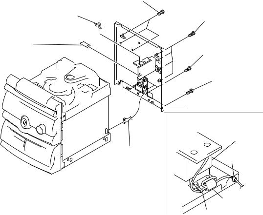
3-1. BACK PANEL
5 Connector (CN9001)
6Flat type wire (15 core)
1Three screws (+BVTP3x8)
2 Four screws (+BVTP3x8)
3 Three screws (+BVTP3x8)
4 Four screws (+BVTP3x8)
8 Back panel
Installing the power cord for the
Chinese model.
Power transformer
7Connector (CN961)
Bushing cord
Ferrite core
Wire clamp
— 7 —
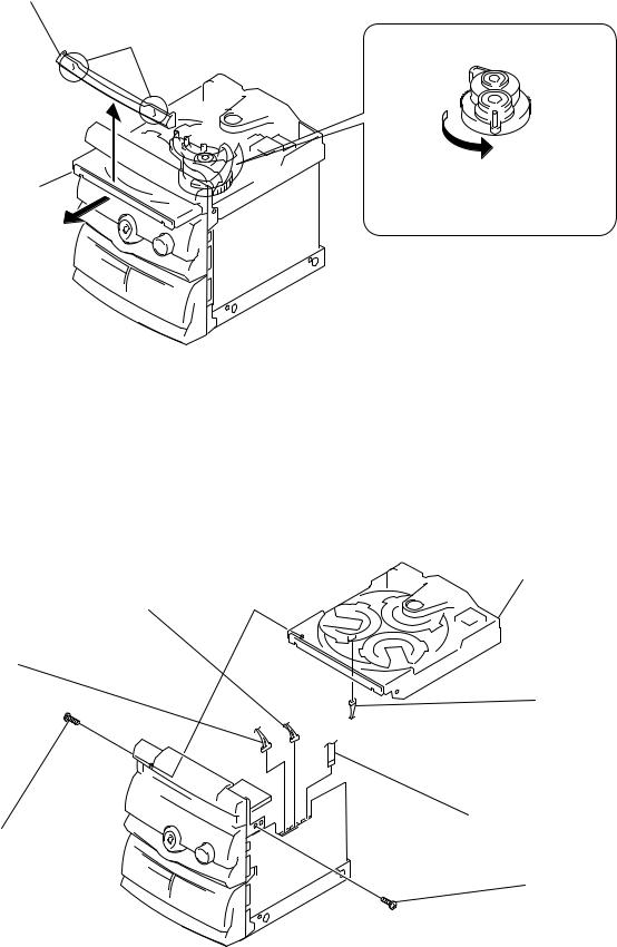
3-2. LOADING PANEL
3 Loading panel
Two claws
1 Turn the cam to the direction of arrow
2 Pull-out the
disc tray.
3-3. CD MECHANISM DECK
7 CD mechanism deck
2Connector (CN830)
3 Connector
(CN820)
6 Connector
(CN901)
1 Flat type wire (13 core)
4Screw (+BVTP3x8)
5 Screw
(+BVTP3x8)
— 8 —
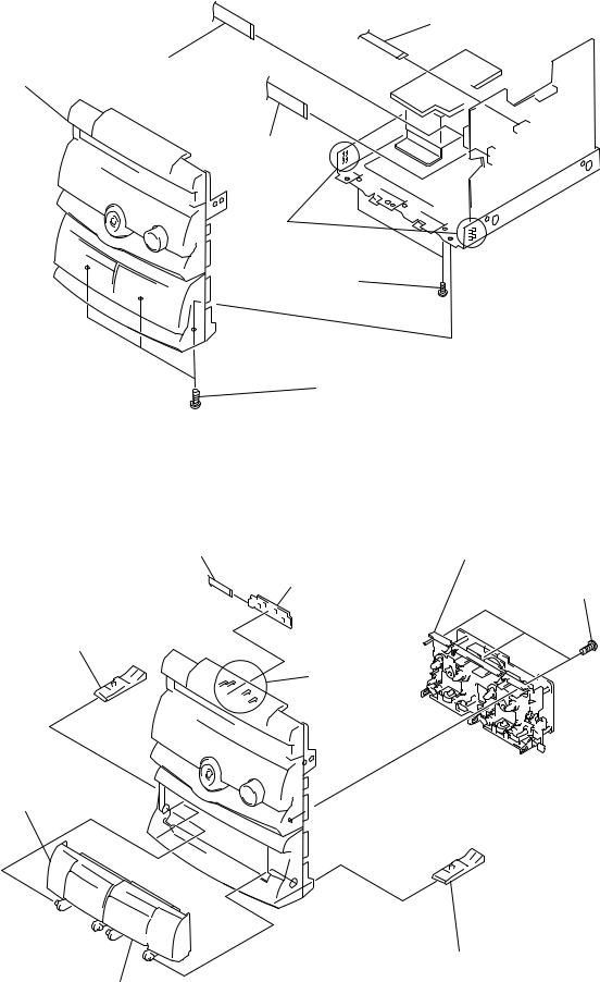
3-4. FRONT PANEL
1 Connector
(CN402)
|
2 Connector |
6 Front panel assembly |
(CN401) |
3 Connector
(CN701)
Two claws
4 Two screws (+BVTT3x6)
5 Three screws (+BVTT3x6)
3-5. TC MECHANISM DECK AND DECO BOARD
1 Push the buttons (EJECT) 4 and 5. |
|
9 Flat type wire (5 core) |
3 TC mechanism deck |
|
8 DECO board |
5 Button (EJECT)
Claws
6 Cassette lid (A) assembly
2Three screws (+BVTP2.6x8)
4 Button (EJECT)
7 Cassette lid (B) assembly
— 9 —
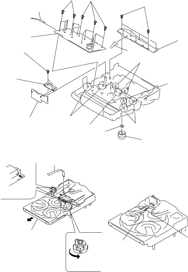
3-6. HP/MIC BOARD, DISPLAY BOARD AND TC SW BOARD
7 Seven screws |
8 Nine screws |
(+BVTP2.6x8) |
(+BVTP2.6x8) |
6 Flat type wire (10 core)
!£ Display board
1 Two screws
(+BVTP2.6x8)
2 Bracket (HP)
3 HP/MIC board |
9 Two claws |
|
0 Two claws
5 Nut
3-7. DISC TRAY
(Perform after removing the front panel.)
3 Flat type wire (8 core)
!¢ Seven screws
(+BVTP2.6x8)
!¤ TC SW board
!¦ Connector
(CN607)
!° Two claws
!ª Claw
!Á Two claws
4 Knob (Vol)
Note: When installing the Disc tray, pull around the flat type wire to pass through the claw A and claw B, as shown in the figure.
4 Push the claws
2 Pull-out the disc tray.
5 Remove the disc tray.
Claw B
Claw A
1Turn the cam to the direction of arrow.
— 10 —
SECTION 4 TEST MODE
VIDEO CD COLOR-BARS MODE
On this mode, the data of the color-bars signal as a picture signal and the 1kHz sine wave signal as a sound signal are output by the mechanism control microcomputer (IC701) for video CD signal check. When measurement of the voltage and waveform on the VIDEO board, perform it in this mode.
For refernce, the color-bars signal can be observed at J9001 (VIDEO OUT) and the sound signal can be observed at J101 (VIDEO/MD (AUDIO) OUT) using an oscilloscope.
1.Connect the lead wire to both ends of the land of SL701 (CAL BAR) of the VIDEO board.
2.Turn the power on. Press FUNCTION button to select CD.
3.After 2 or 3 seconds later, connect the lead wire.
4.After measuring, remove the lead wire connected.
NOTE:
The 1 kHz sine wave is not outputted when the CD is played once, but it is not error.
E-F BALANCE MODE
• Refer to SECTION 6 ELECTRICAL ADJUSTMENTS page 15.
1.Connect the lead wire to both ends of the land of SL702 (ADJ) and SL703 (AFADJ) of the VIDEO board.
2.Turn the power on. Press FUNCTION button to select CD.
3.Short-circuit the lead wire. (At this time, “DISC” on the fluorescent indicator tube will blink (test mode). If it is not blinking, perform from step 1 again.)
4.Press the á button in playback.
5.Every pressing the REPEAT button, the tracking servo and the sledding servo are turned on or off.
6.When the servo is OFF, the counter on front panel will not be changed.
7.After measuring, remove the lead wire connected step 1.
[VIDEO BOARD] (SIDE B)
 SL703 (AFADJ)
 SL702 (ADJ)
 IC751
IC751
IC251 
SL701 (CAL BAR)
— 11 —
SECTION 5
MECHANICAL ADJUSTMENTS
Precaution
1.Clean the following parts with a denatured alcohol-moistened swab:
record/playback heads |
pinch rollers |
erase head |
rubber belts |
capstan |
idlers |
2.Demagnetize the record/playback head with a head demagnetizer.
3.Do not use a magnetized screwdriver for the adjustments.
4.After the adjustments, apply suitable locking compound to the parts adjusted.
5.The adjustments should be performed with the rated power supply voltage unless otherwise noted.
Torque Measurement
Torque |
Torque meter |
Meter reading |
|
|
|
|
|
FWD |
CQ-102C |
36 to 61 g • cm |
|
(0.5 - 0.84 oz • inch) |
|||
|
|
||
|
|
|
|
FWD |
CQ-102C |
2 to 6 g • cm |
|
back tension |
(0.02 - 0.08 oz • inch) |
||
|
|||
|
|
|
|
REV |
CQ-102RC |
36 to 61 g • cm |
|
(0.5 - 0.84 oz • inch) |
|||
|
|
||
|
|
|
|
REV |
CQ-102RC |
2 to 6 g • cm |
|
back tension |
(0.02 - 0.08 oz • inch) |
||
|
|||
|
|
|
|
FF/REW |
CQ-201B |
61 to 143 g • cm |
|
(0.85 - 1.99 oz • inch) |
|||
|
|
||
|
|
|
|
FWD tension |
CQ-403A |
100 g or more |
|
(3.53 oz or more) |
|||
|
|
||
|
|
|
|
REV tension |
CQ-403R |
100 g or more |
|
(3.53 oz or more) |
|||
|
|
||
|
|
|
SECTION 6
ELECTRICAL ADJUSTMENTS
DECK SECTION |
|
0 dB=0.775V |
|
|
|
1.Demagnetize the record/playback head with a head damagnetizer.
2.Do not use a magnetized screwdriver for the adjustments.
3.After the adjustments, apply suitable locking compound to the parts adjusted.
4.The adjustments should be performed with the rated power supply voltage unless otherwise noted.
5.The adjustments should be performed in the order given in this service manual. (As a general rule, playback circuit adjustment should be completed before performing recording circuit adjustment.)
6.The adjustments should be performed for both L-CH and R-CH.
7.Switches and controls should be set as follows unless otherwise specified.
Tape |
Signal |
Used for |
|
|
|
P-4-A100 |
10 kHz, –10 dB |
Azimuth Adjustment |
|
|
|
WS-48B |
3 kHz, 0 dB |
Tape Speed Adjustment |
|
|
|
P-4-L300 |
315 Hz, 0 dB |
Level Adjustment |
|
|
|
NOTE:
Set the test mode by following step before performing the adjustment of “DECK SECTION”. All effects for the output signal are canceled. If the adjustment is not performed in this test mode, you cannot adjust correctly.
Procedure :
With the power turned ON, press the NEXT button, ENTER/
 NEXT button, and EFFECT ON/OFF button simultaneously.
(The “VOLUME” on the fluorescent display tube will blink while in the test mode.)
To exit the test mode, press the POWER button.
Record/Playback Head Azimuth Adjustment
(Deck A, Deck B)
Note: Perform this adjustments for both decks.
Procedure:
1. Mode : Playback
test tape |
|
P-4-A100 |
|
(10kHz, –10dB) |
level meter |
|
|
|
VIDEO/MD |
set |
(AUDIO) OUT |
+ |
|
|
– |
— 12 —
2.Turn the adjustment screw and check output peaks. If the peaks do not match for L-CH and R-CH, turn the adjustment screw so that outputs match within 1 dB of peak.
L-CH |
output |
|
|
|
peak |
within |
|
|
|
level |
|
|
||
|
|
|
||
|
|
1 dB |
|
within 1dB |
|
R-CH |
|
|
|
screw |
peak |
|
|
|
|
|
|
|
|
position |
|
|
|
screw |
|
|
L-CH |
R-CH |
|
|
|
position |
||
|
|
peak |
peak |
|
3. Mode: Playback
test tape P-4-A100 (10kHz, –10dB)
VIDEO/MD |
|
(AUDIO) OUT |
oscilloscope |
|
|
GND |
|
L |
|
set |
|
R |
|
Waveform of oscilloscope
in phase 45° |
90° |
135° 180° |
good |
|
wrong |
4.After the adjustments, apply suitable locking compound to the parts adjusted.
Adjustment Location: Playback Head (Deck A)
Record/Playback/Erase Head (Deck B)
forward
reverse
Tape Speed Adjustment (Deck A)
Note: Set the test mode using the following method and begin tape speed adjustment.
In the test mode, the tape will move at double speed while the HIGH SPEED DUBBING button is pressed.
Procedure :
With the power turned ON, press the NEXT button, ENTER/
 NEXT button, and EFFECT ON/OFF button simultaneously.
(The “VOLUME” on the fluorescent display tube will blink while in the test mode.)
To exit the test mode, press the POWER button.
1.Load WS-48B into deck A and a recordable tape into deck B.
2.Press the rREC button, and press the á button of deck B to set deck B into the recording state.
3.Play deck A.
4.While pressing the HIGH SPEED DUBBING button, set double speed play.
5.Adjust RV652 of the AUDIO board so that the reading of the frequency counter becomes 6000 ± 90 Hz.
6.Release the HIGH SPEED DUBBING button to set normal speed play.
7.Adjust RV651 of the AUDIO board so that the reading of the frequency counter becomes 3000 ± 90 Hz.
Adjustment Location: AUDIO board
Sample Value of Wow and flutter
W.RMS (JIS) less than 0.3% (test tape: WS-48B)
Playback Level Adjustment (Deck A, Deck B)
Procedure:
test tape P-4-L300 (315Hz, 0dB)
level meter
set
VIDEO/MD (AUDIO) OUT
Mode: Playback
Deck A is RV311 (L-CH) and RV411 (R-CH), deck B is RV301 (L-CH) and RV401 (R-CH)
so that adjustment within the following adjustment level.
Adjustment level:
J101 playback level: 301.5 to 338.3 mV (–8.2 to –7.2 dB) level difference between the channels: within ± 0.5 dB
Adjustment Location: AUDIO board
— 13 —
Record Bias Adjustment (Deck B)
Procedure:
INTRODUCTION
When set to the test mode performed in Tape Speed Adjustment, when the tape is rewound after recording, the “REC memory mode” which rewinds only the recorded portion and playback is set.
This “REC memory mode” is convenient for performing this adjustment. During recording, the input signal FUNCTION will automatically switch to VIDEO.
1.Press FUNCTION button to select VIDEO. (This step is not necessary if the above test mode has already been set.)
2.Load a tape into deck B, and press the rREC button.
3.Mode: Record
VIDEO/MD (AUDIO) IN
1)315Hz } 50 mV (–23.8 dB)
2)10kHz
AF OSC |
blank tape |
|
600 Ω |
||
CS-123 |
||
attenuator |
|
|
|
set |
4. Mode: Playback
recorded |
level meter |
position |
|
|
set |
|
VIDEO/MD |
|
(AUDIO) OUT |
Record Level Adjustment (Deck B)
Procedure:
INTRODUCTION
When set to the test mode performed in Tape Speed Adjustment, when the tape is rewound after recording, the “REC memory mode” which rewinds only the recorded portion and playback is set.
This “REC memory mode” is convenient for performing this adjustment. During recording, the input signal FUNCTION will automatically switch to VIDEO.
1.Press FUNCTION button to select VIDEO. (This step is not necessary if the above test mode has already been set.)
2.Load a tape into deck B, and press the rREC button.
3.Mode: Record
VIDEO/MD (AUDIO) IN 315Hz 50 mV (–23.8 dB)
AF OSC |
blank tape |
|
600 Ω |
||
CS-123 |
||
attenuator |
|
|
|
set |
4. Mode: Playback
recorded |
level meter |
position |
|
|
set |
|
VIDEO/MD |
|
(AUDIO) OUT |
5.Confirm playback the signal recorded in step 2 become adjustment level as follows.
If these levels do not adjustment level, adjust the RV341 (L- CH) and RV441 (R-CH) on the AUDIO board to repeat steps 3 and 4.
Adjustment level: The playback output of 10 kHz level difference against 315 Hz reference should be ± 1.0 dB.
Adjustment Location: AUDIO board
5.Confirm playback the signal recorded in step 2 become adjustment level as follows.
If these levels do not adjustment level, adjust the RV301 (L- CH) and RV351 (R-CH) on the MAIN board to repeat steps 3 and 4.
Adjustment level:
CN403 playback level: 47.2 to 53.0 mV (–24.3 to –23.3 dB)
Adjustment Location: MAIN board
|
|
RV301 |
Adjustment Location |
[MAIN BOARD] (Component Side) |
Record Level (L CH) |
|
||
[AUDIO BOARD] (Conductor Side) |
|
|
RV341 (Lch), RV441 (Rch) |
|
|
||
Record Bias |
|
|
IC401 |
|
|
|
|
|
|
RV301 |
|
RV651 (Normal Speed) |
RV651 RV652 |
|
RV401 |
|
RV652 (High Speed) |
|
|
|
Tape Speed |
|
RV351 |
|
RV441 |
RV341 |
|
RV311 |
Record Level |
|
|
|
(R CH) |
|
|
|
|
|
|
RV301 (Lch), RV401 (Rch) |
|
RV411 |
|
|
Playback Level (Deck B) |
RV311 (Lch), RV441 (Rch) |
|
||
|
|
|
||
|
|
Playback Level (Deck A) |
|
|
— 14 —

CD SECTION
NOTE :
1.CD Block is basically designed to operate without adjustment. Therefore, check each item in order given.
2.Use YEDS-18 disc (3-702-101-01) unless otherwise indicated.
3.Use an oscilloscope with more than 10MW impedance.
4.Clean the object lens by an applicator with neutral detergent when the signal level is low than specified value with the following checks.
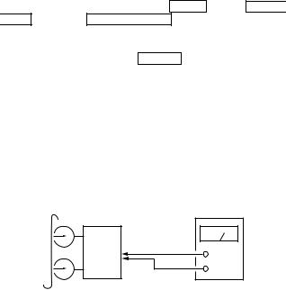
S Curve Check
|
oscilloscope |
BD board |
|
TP (FE) |
+ |
TP (VC) |
– |
Procedure :
1.Connect oscilloscope to test point TP (FE) on BD board.
2.Connect between test point TP (FEI) and TP (VC) by lead wire.
3.Turned Power switch on.
4.Put disc (YEDS-18) in and turned Power switch on again and actuate the focus search. (actuate the focus search when disc table is moving in and out.)
5.Check the oscilloscope waveform (S-curve) is symmetrical between A and B.
And confirm peak to peak level within 3±1 Vp-p.
S-curve waveform
symmetry
A
Within 3 ± 1 Vp-p
B
6. After check, remove the lead wire connected in step 2.
Note : • Try to measure several times to make sure than the ratio of A : B or B : A is more than 10 : 7.
• Take sweep time as long as possible and light up the brightness to obtain best waveform.
RF Level Check
|
oscilloscope |
BD board |
|
TP (RF) |
+ |
TP (VC) |
– |
Procedure :
1.Connect oscilloscope to test point TP (RF) on BD board.
2.Turned Power switch on.
3.Put disc (YEDS-18) in to play the number five track.
4.Confirm that oscilloscope waveform is clear and check RF signal level is correct or not.
Note : A clear RF signal waveform means that the shape “ à” can be clearly distinguished at the center of the waveform.
RF signal waveform
VOLT/DIV : 200mV
TIME/DIV : 500ns
level : 1.3 +0.25–0.20 Vp-p
E-F Balance (1 Track Jump) check (Without remote commander)
oscilloscope
BD board |
|
TP (TE) |
+ |
TP (VC) |
– |
Procedure:
1.Connect oscilloscope to test point TP (TE) on BD board.
2.Turned Power switch on. Press FUNCTION button to select CD.
3.Put disc (YEDS-18) in to play the number five track.
4.Press the “ P(Pause)” button.
5.Check the level B of the oscilloscope's waveform and the A (DC voltage) of the center of the Traverse waveform.
Confirm the following:
•A/B x 100 = less then ± 22 (%)
1 track jump waveform
Center of the waveform
B |
A (DC voltage) |
0V |
Symmetry |
level : 1.3 ± 0.6 Vp-p |
E-F Balance (Traverse) Check (With remote commander)
oscilloscope
BD board |
|
TP (TE) |
+ |
TP (VC) |
– |
Procedure :
1.Connect oscilloscpe to test point TP (TE) on BD board.
2.Connect the lead wire to both ends of the land of SL702 (ADJ) and SL703 (AFADJ) of the VIDEO board.
3.Turned Power switch on. Press FUNCTION button to select CD.
4.Short the lead wire.
5.Put disc (YEDS-18) in to play the number five track.
6.Press the REPEAT button. (The tracking servo and the sledding servo are turned OFF.)
— 15 —
7.Check the level B of the oscilliscope's waveform and the A (DC voltage) of the center of the Traverse waveform.
Confirm the following : A/B x 100 = less than ± 22%
Traverse waveform
|
Center of the waveform |
|
B |
0V |
A (DC voltage) |
|
|
|
level : 1.3 ± 0.6 Vp-p |
8.Press the REPEAT button. (The tracking servo and sledding servo are turned ON.) Confirm the C (DC voltage) is almost equal to the A (DC voltage) is step 7.
Traverse waveform
|
C (DC |
0V |
voltage) |
Tracking servo |
Tracking servo |
Sled servo |
Sled servo |
OFF |
ON |
9. Remove the lead wire connected step 1.
Adjustment Location :
[ BD BOARD ] — SIDE A —
1 20
(FE)
IC103 (RF) |
(FEI) |
1011 (TE) (VC)
(PLCK)
IC101
RF PLL Free-run Frequency Check
Procedure :
1. Connect frequency counter to TP (PLCK) with lead wire.
frequency counter
BD board |
|
TP (PLCK) |
+ |
|
– |
2.Turned Power switch on.
3.Put the disc (YEDS-18) in to play the number five track. Confirm that reading on frequency counter is 4.3218MHz.
VIDEO SECTION
Frequency adjustment
1.Connect the frequency counter to check point of the VIDEO board.
2.Adjust CT401 of the VIDEO board so that the frequency counter read 13.5MHz ± 40Hz at STOP condition.
frequency counter
VIDEO board
TP410 (DCLK)
+
–
[ VIDEO BOARD ] — SIDE B —
 SL703 (AFADJ)
SL702 (ADJ)
CT401
Frequency
 IC751
IC751
IC251 
SL701 (CAL BAR) |
TP410 (DCLK) |
— 16 —
SECTION 7
DIAGRAMS
7-1. CIRCUIT BOARDS LOCATION
CD SW board
PANEL board (including pB)
HP/ MIC board
TC SW board
pB
CONNECTOR board
SENSOR board
VIDEO OUT board
ENCAPSULATED
COMPONENT
KEY CON board
Note: pA is including in AUDIO board. pB is including in PANEL board.
MAIN board
DECO board
SURROUND board
TRANS board
pA
MOTOR board
LEAF SWITCH board
POWER board
AUDIO board (including pA)
MOTOR (TURN) board
BD board
VIDEO board |
MOTOR (SLIDE) board |
VIDEO POWER board
— 17 —
HCD-V909AV
7-2. BLOCK DIAGRAMS
— KEY CON SECTION —
|
MIC AMP |
ECHO AMP |
||
J751 |
IC750 (1/2) |
IC750 (2/2) |
||
|
|
|
|
|
MIX MIC |
3 |
1 |
6 |
7 |
|
|
|
RV750 |
|
|
|
|
MIC LEVEL |
|
|
|
|
|
ECHO |
|
|
|
|
IC751 |
1 |
2 |
9 |
|
8 |
LPF1 |
|
|
LPF2 |
RV751 |
|
|
|
||
|
|
|
|
ECHO LEVEL |
|
|
|
SWITCH |
|
|
|
|
|
IC1403 |
|
|
|
|
|
5 |
4 |
L IN |
|
|
|
3 |
||
|
|
|
|
|
|
KEY CONTROL |
9 |
10 11 |
|
||
|
|
|
|||
IC1401 |
|
|
|
|
|
LPF1 |
|
MIX |
Q1401 |
|
K CON |
IN |
|
OUT |
15 |
|
|
22 |
|
|
|
|
|
Rch |
CLOCK |
STORBE |
|
|
A |
|
|
MAIN |
|||
DATA |
|
|
|||
|
|
SECTION |
|||
7 |
8 |
9 |
|
|
(Page 25) |
|
|
|
|||
|
|
|
|
|
LATCH |
|
|
|
|
|
CLK |
|
|
|
|
|
DATA |
|
|
|
|
|
L OUT |
09
• R CH : Same as Lch
• Signal path
 : FM : MIC
— 18 —
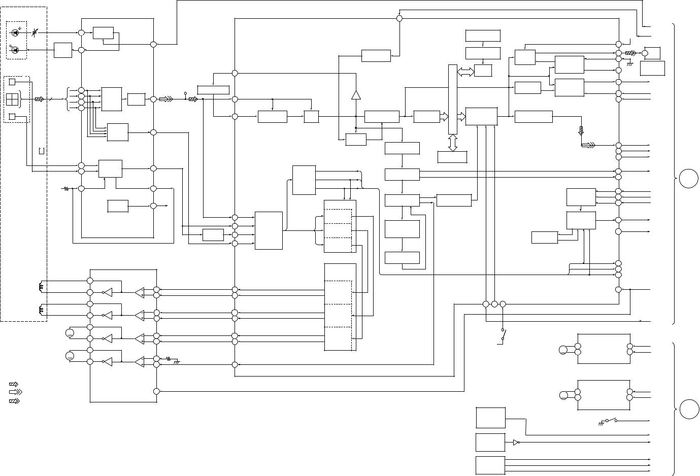
HCD-V909AV
— CD SECTION —
OPTICAL PICK-UP |
|
|
|
|
|
|
|
|
|
|
|
|
|
|
|
|
|
|
|
|
|
|
|
|
||
BLOCK (KSS-213D/Q-NP) |
|
|
|
|
|
|
|
DIGITAL SERVO |
|
|
|
|
|
|
|
|
|
|
|
|
|
|
|
|||
|
|
|
|
|
RF AMP |
|
|
|
|
|
|
|
|
|
|
|
|
|
|
|
|
|
|
|
||
|
LASER |
|
|
|
|
|
|
DIGITAL SIGNAL PROCESSOR |
|
|
|
|
|
|
|
|
|
|
|
|
|
|
|
|||
|
|
|
|
IC103 |
|
|
|
|
|
IC101 |
|
|
62 |
|
|
|
|
|
|
|
|
|
|
|
|
|
|
DIODE |
LD |
|
|
|
|
|
|
|
|
|
|
|
|
|
|
|
|
|
|
|
|
|
|
|
|
|
|
|
|
|
|
|
|
|
|
|
|
|
XTAL |
|
|
|
|
|
|
|
|
|
|
|
|
|
PD |
POWER |
|
|
|
|
|
|
|
|
|
|
|
|
|
|
|
|
|
|
|
|
|
LDON |
|
||
|
|
2 |
APC LD |
|
|
|
|
|
|
|
|
|
|
|
|
|
|
|
|
|
|
|
||||
|
|
|
|
|
|
|
|
|
|
|
|
|
|
PRIORITY |
|
|
|
|
|
|
|
|
|
|||
|
|
|
|
AMP |
|
|
|
|
|
|
|
|
|
|
|
|
|
|
|
|
+5V |
384FS |
|
|||
|
|
|
|
|
|
|
|
|
|
|
|
|
|
|
EMCODER |
|
|
|
|
|
|
|
||||
|
|
|
|
|
|
|
|
|
|
|
|
|
|
|
|
|
|
|
|
MD2 |
|
|
|
|
||
|
LD |
LD |
|
|
|
19 |
|
|
|
|
|
|
|
|
|
|
|
|
|
|
70 |
|
IC841 |
|
||
|
DRIVE |
1 |
|
|
|
|
|
|
|
|
|
|
|
ADDRESS |
|
|
|
|
DOUT |
|
|
|
|
|||
|
|
|
|
|
|
|
|
|
|
|
|
CLOCK |
|
|
|
|
|
71 |
|
1 |
|
|||||
|
|
|
Q101 |
|
|
|
|
|
|
|
|
|
|
|
GENERATOR |
DIGITAL |
|
|
|
EXCK |
|
|
||||
|
|
|
|
|
|
|
|
|
|
|
|
|
|
GENERATOR |
|
|
|
OUT |
SUBCODE |
|
76 |
|
CD |
|
||
|
|
|
|
|
|
|
|
|
|
|
|
|
|
|
|
32K |
|
|
|
P-W |
|
SBSO |
|
|
|
|
|
|
|
|
|
|
|
|
|
|
ASY0 |
|
|
|
|
|
|
|
PROCESSOR |
|
75 |
|
DIGITAL OUT |
|
|||
DETECTOR |
|
|
|
|
|
|
39 |
|
|
|
|
|
RAM |
|
|
|
|
|
|
|
OPTICAL |
|
||||
|
E |
|
|
|
|
|
|
|
|
|
|
|
|
|
|
|
|
PEAK |
SUBCODE |
|
SUBQ |
77 |
|
SUBQ |
|
|
|
|
|
|
|
|
|
RF |
|
|
|
|
|
|
|
|
|
|
|
Q |
|
|
|
|
|
|
|
|
|
|
|
3 |
|
|
INTEGRATOR |
|
|
|
|
|
|
|
BUS |
|
DETECTOR |
|
|
SQCK |
|
|
|
|
||
|
|
|
4 |
RF |
|
|
|
|
|
|
|
|
|
PROCESSOR |
|
78 |
|
SQCK |
|
|||||||
A |
C |
|
4 |
RF FQ |
|
|
|
RF AC |
|
|
|
|
|
|
|
|
|
|
|
|||||||
|
16 |
|
36 |
|
|
|
|
|
|
|
|
|
|
SCLK |
|
|
||||||||||
|
|
SUMMING |
|
|
|
|
|
|
DATA |
|
|
|
|
|
83 |
|
SCLK |
|
||||||||
B |
D |
|
|
5 |
AMP |
AMP |
|
|
|
|
|
|
|
|
|
|
|
|
|
|
|
|
|
|
|
|
|
|
|
|
6 |
|
|
|
|
|
|
|
|
|
|
|
|
|
|
|
|
|
|
|
|
|
|
|
|
|
|
|
|
|
|
|
|
|
|
|
|
|
D/A |
|
|
|
|
|
|
|
|
|
|
|
|
|
|
|
|
|
|
|
|
|
ASY1 |
ASYMMETRY |
|
|
EFM |
|
|
SERIAL/PARALLEL |
|
|
|
|
|
|
|
|
|
|
F |
|
|
|
|
|
|
|
38 |
MIX |
|
REGISTER |
DATA |
|
|
|
|
|
|
|
|
|
||||
|
|
|
|
|
|
|
|
|
CORRECTION |
|
DEMODULATOR |
|
PROCESSOR |
|
|
|
|
|
|
|
|
|||||
|
|
|
|
|
|
|
|
|
|
|
|
|
|
PROCESSOR |
|
|
|
|
|
|
|
|
||||
|
|
|
|
|
|
|
|
|
|
|
|
|
|
|
|
|
|
|
|
|
|
|
|
|
||
|
|
|
|
|
FOCUS |
|
|
|
|
|
|
|
|
|
|
|
|
|
|
|
|
|
|
|
|
|
|
|
|
|
|
ERROR |
|
15 |
|
|
|
|
|
|
|
|
|
|
|
|
|
|
|
|
|
|
|
|
|
|
|
|
AMP |
|
|
|
|
|
|
|
|
DIGITAL |
|
|
|
|
|
|
|
|
|
|
|
|
|
|
|
|
|
|
|
|
|
|
|
|
|
|
PLL |
|
|
|
|
|
|
|
DATA |
46 |
|
ADATA |
|
|
|
|
|
|
|
|
|
|
|
|
|
|
|
SYNC |
|
|
|
|
|
|
|
|
|
|||
|
|
1 |
|
|
|
|
|
|
|
|
|
|
|
PROTECTOR |
|
ERROR |
|
|
|
|
|
LRCK |
45 |
|
LRCK |
|
|
|
|
|
|
|
|
|
|
|
|
|
|
|
|
|
|
|
|
|
|
BCLK |
47 |
|
BCK |
|
|
|
|
|
|
|
|
|
|
|
|
|
|
|
|
|
|
CORRECTOR |
|
|
|
|
|
|
|
|||
|
|
|
|
|
TRACKING |
|
|
|
|
|
|
|
|
|
|
|
|
|
|
|
|
|
|
|
|
|
|
|
|
|
8 |
|
13 |
|
|
|
|
|
|
|
|
|
|
|
|
|
|
|
|
|
|
|
|
|
|
|
|
ERROR |
|
|
|
|
|
|
FOK |
|
|
|
|
|
|
|
|
SCOR |
|
|
|
|
||
|
|
|
|
9 |
|
|
|
|
|
MIRR |
TIMING |
|
|
|
|
|
|
|
74 |
|
SCOR |
B |
||||
|
|
|
|
AMP |
|
|
|
|
|
|
|
|
|
|
|
|
|
|
WFCK |
|
||||||
|
|
|
|
|
|
|
|
|
|
|
|
DFCT |
DFCT |
GENERATOR 1 |
|
|
|
|
|
|
|
73 |
|
|
||
|
|
|
VC |
|
|
|
|
|
|
|
|
FOK |
MIRR |
|
|
|
|
|
|
|
|
|
|
|
|
|
|
|
|
10 |
|
|
11 |
|
|
|
|
DETECTOR |
|
|
|
|
|
|
|
|
DATA |
|
|
|
|||
|
|
|
|
|
|
|
|
|
|
|
|
|
|
|
|
|
|
|
|
DATA |
|
|||||
|
|
|
|
|
|
|
|
|
|
|
|
|
|
|
|
|
|
CPU |
86 |
|
VIDEO |
|||||
|
|
|
|
|
|
|
|
|
|
|
|
|
|
CLV SERVO |
|
TIMING |
|
|
|
XLT |
87 |
|
XLT |
|||
|
|
|
|
|
|
|
VC |
|
|
|
|
|
|
|
|
|
|
INTERFACE |
CLK |
|
SECTION |
|||||
|
|
|
|
|
VC |
|
|
|
|
|
|
SERVO DSP |
PROCESSOR |
|
GENERATOR 2 |
|
|
|
|
|
88 |
|
CLK |
(Page 21) |
||
|
|
|
|
|
|
|
|
|
|
|
|
|
|
|
|
|
|
|
||||||||
|
|
|
|
|
|
12 |
|
|
|
|
|
|
|
|
|
|
|
|
|
|
|
|
||||
|
|
|
|
|
BUFFER |
|
|
|
|
|
|
|
|
|
|
|
|
|
|
|
|
|
|
|
|
|
|
|
|
|
|
|
|
|
|
26 |
RF DC |
|
|
FOCUS |
|
|
|
|
|
|
SERVO |
SENS |
|
|
|
|
|
|
|
|
|
|
|
|
|
|
TE |
|
|
SERVO |
|
|
|
|
|
|
AUTO |
80 |
|
SENS |
|
|||
|
|
|
|
|
|
|
|
|
27 |
A/D |
|
TRACKING |
1B TIMS |
|
|
|
|
|
SEQUENCER |
|
|
|
|
|
||
|
|
|
|
|
|
|
|
|
|
SE |
|
OVERSAMPLING |
|
|
|
|
|
|
|
C2PO |
56 |
|
C2PO |
|
||
|
|
|
|
|
|
|
|
INTE- |
28 |
CONVERTER |
|
SERVO |
FILTER |
|
|
|
SERVO |
|
|
|
|
|
||||
|
|
|
|
|
|
|
|
GRATOR |
|
|
|
|
|
|
|
|
|
|
|
|
|
|
|
|
||
|
|
|
|
|
|
|
|
|
FE |
|
|
|
|
|
|
|
INTERFACE |
|
|
|
|
|
|
|
|
|
|
|
|
|
|
|
|
|
|
29 |
|
|
SLED |
|
|
|
|
|
|
|
|
|
|
|
|
||
|
|
|
|
|
|
|
|
|
|
|
|
|
|
|
|
|
|
|
|
|
|
|
|
|||
|
|
|
|
|
|
|
|
|
|
|
|
|
SERVO |
|
|
|
|
|
|
|
|
|
|
|
|
|
|
|
|
|
|
FOCUS/TRACKING COIL DRIVE |
|
|
|
|
|
|
|
NOISE |
|
|
|
|
|
|
|
|
|
|
|
|
|
|
|
|
|
|
SPINDLE/SLED MOTOR DRIVE |
|
|
|
|
|
|
|
SHAPER |
|
|
|
|
|
|
|
FOK |
93 |
|
|
|
|
|
|
|
|
|
IC102 |
|
|
|
|
|
|
|
|
|
|
|
|
|
|
|
|
DFCT |
92 |
|
|
|
|
|
|
|
|
|
|
|
|
|
|
|
|
|
|
|
|
|
|
|
|
|
|
|
|
||
|
|
|
|
T+ |
|
|
|
|
|
|
|
|
PWM |
|
|
|
|
|
|
|
|
MIRR |
91 |
|
|
|
|
|
|
|
1 |
|
|
|
|
|
|
|
GENERATOR |
|
|
|
|
|
|
|
|
|
|
|
|
|
|
|
TRACKING |
|
|
|
|
|
|
|
|
|
|
|
|
|
|
|
|
|
|
|
|
|
|
|
||
|
|
|
|
|
|
|
|
TFDR |
|
|
TRACKING |
|
|
|
|
|
|
|
|
|
|
|
|
|
||
|
|
COIL |
|
T– |
|
|
4 |
|
4 |
|
|
|
|
MUTE |
|
S STOP |
|
|
|
XRST |
81 |
|
XRST |
|
||
|
|
|
|
2 |
|
|
TRDR |
|
|
PWM |
|
|
GFS |
|
|
|
|
|
||||||||
|
|
|
|
|
|
5 |
|
6 |
|
|
|
|
|
|
|
|
|
|
|
|
||||||
|
|
|
|
F+ |
|
|
|
|
|
|
GENERATOR |
|
|
|
|
|
|
|
|
|
|
|||||
|
|
|
|
16 |
|
|
|
|
|
|
|
|
|
|
79 |
54 |
99 |
|
|
|
|
|
|
|
|
|
|
FOCUS |
|
|
|
|
|
|
|
|
|
|
|
|
|
|
|
|
|
|
|
|
|||||
|
|
|
|
|
|
|
|
FFDR |
|
|
FOCUS |
|
|
|
|
|
|
|
|
|
|
|
|
|
||
|
|
COIL |
|
F– |
|
|
19 |
|
8 |
|
|
|
|
|
|
|
|
|
|
|
|
|
|
|
||
|
|
|
17 |
|
|
FRDR |
|
|
PWM |
|
|
|
|
|
|
|
|
|
|
|
|
|
||||
|
|
|
|
|
|
|
|
|
|
|
|
|
|
|
|
|
|
|
|
|
||||||
|
|
|
|
|
|
20 |
|
10 |
|
|
GENERATOR |
|
|
|
|
|
|
|
|
|
|
|
AMUTE |
|
||
|
|
|
|
|
|
|
|
|
|
|
|
|
|
|
|
|
|
|
|
|
|
|
|
|
|
|
|
|
|
M102 |
|
13 |
|
|
|
|
|
|
|
|
|
|
|
|
S901 |
|
|
|
|
|
|
|
|
|
|
|
SLED |
M |
|
|
10 |
|
2 |
SRDR |
|
|
SLED |
|
|
|
|
LIMIT |
|
|
|
|
|
|
|
|
|
|
|
MOTOR |
|
12 |
|
|
SFDR |
|
|
|
|
|
|
SWITCH |
|
|
|
|
|
|
|
|
|||
|
|
|
|
|
|
|
|
PWM |
|
|
|
|
|
|
|
|
|
|
|
|
||||||
|
|
|
|
|
|
9 |
|
100 |
|
|
|
|
|
+5V |
M701 |
|
|
|
|
|
|
|
|
|||
|
|
|
|
|
|
|
|
|
|
|
|
|
GENERATOR |
|
|
|
|
7 |
OUT1 |
|
IN1 |
3 |
TBL.L |
|
||
|
|
|
M101 |
|
27 |
|
|
|
|
|
|
|
|
|
|
|
|
TURN |
M |
|
|
|||||
|
|
|
|
|
|
|
|
|
|
|
|
|
|
|
|
2 |
OUT2 |
TURN |
IN2 |
6 |
TBL.R |
|
||||
|
|
|
SPINDLE |
M |
|
|
|
|
|
|
|
|
|
|
|
|
|
MOTOR |
|
|
||||||
|
|
|
|
|
23 |
|
|
|
|
|
|
|
|
|
|
|
|
|
MOTOR DRIVER |
|
|
|
||||
|
|
|
MOTOR |
|
26 |
|
|
|
MDP |
|
|
|
|
|
|
|
|
|
|
|
IC701 |
|
|
|
|
|
|
|
|
|
|
|
24 |
|
96 |
|
|
|
|
|
|
|
|
|
|
|
|
|
|
|
|||
• R CH: Same as L ch |
|
|
|
|
|
|
|
|
|
|
|
|
|
|
|
|
|
|
|
|||||||
|
|
|
|
|
|
|
|
|
|
|
|
|
|
|
|
|
|
|
|
|
|
|
||||
• SIGNAL PATH |
|
|
|
|
|
|
|
|
|
|
|
|
|
|
|
|
|
|
|
|
|
|
|
|
||
|
|
: CD |
|
|
|
|
|
|
|
|
|
|
|
|
|
|
|
M801 |
|
|
|
|
|
|
|
|
|
|
: VIDEO |
|
|
|
MUTE 15 |
|
|
|
|
|
|
|
|
|
|
|
4 |
OUT2 |
|
RIN |
2 |
LOAD IN |
|
||
|
|
|
|
|
|
|
|
|
|
|
|
|
|
|
SLIDE |
M |
|
|
||||||||
|
|
: CD (Digital) |
|
|
|
|
|
|
|
|
|
|
|
|
|
|
MOTOR |
7 |
OUT1 |
SLIDE |
FIN |
10 |
LOAD OUT |
|
||
|
|
|
|
|
|
|
|
|
|
|
|
|
|
|
|
|
|
|||||||||
|
|
|
|
|
|
|
|
|
|
|
|
|
|
|
|
|
|
|
MOTOR DRIVER |
|
|
C |
||||
|
|
|
|
|
|
|
|
|
|
|
|
|
|
|
|
|
|
|
|
|
|
IC801 |
|
|
|
|
|
|
|
|
|
|
|
|
|
|
|
|
|
|
|
|
TABLE |
|
|
|
S801 |
|
|
|
|
||
|
|
|
|
|
|
|
|
|
|
|
|
|
|
|
|
SENSOR |
|
|
|
|
|
|
|
|||
|
|
|
|
|
|
|
|
|
|
|
|
|
|
|
|
|
|
OPEN/CLOSE |
|
|
|
OPEN |
|
|||
|
|
|
|
|
|
|
|
|
|
|
|
|
|
|
|
IC702 |
|
|
|
|
|
MAIN |
||||
|
|
|
|
|
|
|
|
|
|
|
|
|
|
|
|
|
|
|
|
|
DET |
|
|
|
|
|
|
|
|
|
|
|
|
|
|
|
|
|
|
|
|
|
|
|
|
|
|
|
|
|
|
SECTION |
|
|
|
|
|
|
|
|
|
|
|
|
|
|
|
|
|
|
|
|
|
|
|
|
|
|
|
|
|
|
|
|
|
|
|
|
|
|
|
|
|
|
|
|
DISC |
|
|
|
|
|
|
|
T. SENS |
(Page 25) |
|
|
|
|
|
|
|
|
|
|
|
|
|
|
|
|
|
|
|
|
|
|
|
|
|
|
||
|
|
|
|
|
|
|
|
|
|
|
|
|
|
|
|
SENSOR |
|
|
|
|
|
|
|
DISC SENS |
|
|
|
|
|
|
|
|
|
|
|
|
|
|
|
|
|
|
IC703 |
Q701 |
|
|
|
|
|
|
|
|
|
|
|
|
|
|
|
|
|
|
|
|
|
|
|
|
|
|
|
|
|
|
|
|
|
|
|
|
|
|
|
|
|
|
|
|
|
|
|
|
|
|
|
|
ROTARY |
|
|
|
|
|
|
|
ENC-1 |
|
|
09 |
|
|
|
|
|
|
|
|
|
|
|
|
|
|
ENCODER |
|
|
|
|
|
|
|
ENC-2 |
|
||
|
|
|
|
|
|
|
|
|
|
|
|
|
|
|
|
S811 |
|
|
|
|
|
|
|
ENC-3 |
|
|
|
|
|
|
|
|
|
|
|
|
|
|
|
|
|
|
|
|
|
|
|
|
|
|
|
|
|
|
|
|
|
|
|
|
— 19 — |
|
|
|
|
|
|
|
|
|
|
— 20 — |
|
|
|
|
|
|
|
|

|
|
|
|
|
|
|
|
|
|
|
|
|
|
|
|
|
|
|
|
|
|
|
|
|
|
|
|
|
|
|
|
|
|
|
|
|
|
|
|
|
|
|
|
|
|
HCD-V909AV |
|||
— VIDEO SECTION — |
|
|
|
|
|
|
|
|
|
|
|
|
|
|
|
|
|
|
|
|
|
|
|
|
|
|
|
|
|
|
|
|
|
10BIT VIDEO D/A CONVERTER |
|
|
|
|
|
|
|
|
|
|
|||||
|
|
|
|
|
|
|
|
|
|
|
|
|
|
|
|
|
|
|
|
|
|
|
|
|
|
|
|
|
|
|
|
|
|
|
|
|
|
|
|
|
|
|
|
|
|
||||
|
|
|
|
|
|
|
|
|
|
|
|
|
|
|
|
|
|
|
|
|
|
|
|
|
|
|
|
|
|
|
|
|
|
|
|
|
|
IC401 |
|
|
|
|
|
|
|
|
|
|
|
|
|
|
|
|
|
|
|
|
|
|
|
MPEG DECODER |
|
|
|
|
|
|
|
|
|
|
|
NOISE REDUCTION |
|
|
|
|
|
|
|
|
|
|
|
|
|
|
|
|
VIDEO AMP |
|
|
||||||
|
|
|
|
|
|
|
|
|
|
|
|
|
IC201 |
|
|
|
|
|
|
|
|
|
|
|
|
IC301 |
|
|
|
|
|
|
|
|
|
|
|
|
|
|
|
|
|
J9001 |
|||||
|
|
|
|
|
|
|
|
|
|
|
|
|
|
|
|
|
|
|
|
|
|
|
|
|
|
|
|
|
|
|
|
|
|
|
|
|
|
|
|
|
|
IC451 |
|
||||||
|
|
|
|
|
|
|
|
|
|
|
|
|
|
|
|
|
|
|
|
|
|
|
|
|
|
|
|
|
|
|
|
|
|
|
|
|
|
|
|
|
|
|
|
|
|
VIDEO OUT |
|||
|
|
|
BUFFER |
|
|
|
|
|
|
|
|
|
|
|
|
|
|
|
|
|
|
|
|
|
|
|
|
|
|
|
|
|
|
|
|
|
|
|
|
|
|
|
|
|
|
|
|||
|
|
|
|
|
|
|
|
|
|
|
|
|
|
|
|
|
|
|
71 |
|
|
|
1 |
|
|
|
|
1 |
|
|
|
|
|
|
|
|
|
|
|
|
V |
24 |
5 |
|
7 |
|
|
||
|
|
|
IC501 (1/2) |
|
|
|
|
|
|
|
|
|
|
|
|
|
|
|
|
|
Y0-Y7 |
|
|
|
|
|
|
|
|
|
|
|
|
|
|
|
|
|
|
|
|
||||||||
|
|
|
|
|
|
|
|
|
|
|
|
|
|
|
|
|
|
|
|
|
|
|
|
|
|
60 |
|
|
|
|
|
|
|
|
|
|
|
Y, C/Y, U, V |
|
|
|
|
|||||||
|
|
|
|
|
|
|
|
|
|
|
|
|
|
|
|
|
|
|
Y |
|
74 |
|
|
4 |
Y |
|
|
4 |
|
|
|
|
|
|
|
|
|
|
|
|
|
|
|
|
|
||||
|
|
|
|
|
|
|
|
|
|
|
|
|
|
|
|
|
|
|
|
|
|
|
|
|
|
|
|
|
|
|
LPF |
|
|
|
|
|
|
|
|
|
|
||||||||
|
BCK |
|
9 |
|
11 |
|
112 |
|
|
MPEG |
|
|
MPEG |
|
VIDEO |
|
|
|
• |
|
|
|
• |
|
|
|
67 |
• |
|
|
DEMPX, LEVEL |
|
|
|
MODULATOR |
|
SELECTOR |
|
|
|
|
|
|
|
|||||
B |
ADATA |
8 |
|
12 |
|
111 |
CD-ROM |
|
|
|
|
|
|
76 |
|
|
|
6 |
RGB-YUV |
NOISE |
YUV-RGB |
6 |
|
|
|
|
|
|
|
& |
Y |
|
|
|
|
|
|
||||||||||||
|
|
SYSTEM |
|
|
VIDEO |
POSTPROCESSOR |
|
|
80 |
|
|
|
9 |
|
9 |
|
|
TRANSLATOR |
|
|
LPF |
|
|
|
|
29 |
5 |
|
7 |
|
|
||||||||||||||||||
LRCK |
|
7 |
|
13 |
|
110 |
DECODER |
|
|
|
& |
|
|
|
|
|
|
CONV. |
REDUSER |
CONV. |
|
|
|
& |
|
|
|
|
|
|
|
INTER- |
|
|
|
|
|||||||||||||
|
|
|
DECODER |
|
DECODER |
|
|
|
|
|
|
C0-C7 |
|
|
|
|
|
|
|
|
|
|
|
|
|
|
POLATOR |
|
|
|
|
|
|
|
|||||||||||||||
C2PO |
|
6 |
|
14 |
|
109 |
|
|
|
SYNC GENERATOR |
C |
|
63 |
|
|
11 |
C |
|
|
51 |
11 |
|
INTERPOLTATOR |
|
|
|
|
|
|
|
C |
32 |
3 |
|
1 |
4 |
3 |
||||||||||||
|
|
|
|
|
|
|
|
|
|
|
|
|
|
|
|
|
|
|
|
|
DELAY |
|
|
|
|
|
|
||||||||||||||||||||||
CD |
|
|
|
|
|
|
|
|
|
|
|
|
|
|
|
|
|
|
|
|
70 |
|
|
|
18 |
|
|
|
58 |
18 |
|
|
|
|
|
|
|
|
|
|
|
|
|
||||||
384FS |
|
|
|
|
|
|
|
|
|
|
|
|
|
|
|
|
|
|
XSGRST |
|
|
|
|
|
|
|
|
|
|
|
|
|
|
|
|
|
|
|
|
|
|
|
|||||||
SECTION |
5 |
|
15 |
|
103 |
|
|
|
|
|
|
|
|
|
|
|
|
|
97 |
|
|
|
|
|
|
|
|
|
|
|
|
|
|
|
|
|
|
|
|
|
Y/C AMP |
|
J9002 |
||||||
(Page 20) |
|
|
|
|
|
|
|
|
|
|
|
|
|
|
|
|
|
|
|
|
|
|
|
|
|
|
|
|
|
|
|
|
|
|
|
|
|
|
|
|
|
||||||||
ADATA |
|
|
|
|
100 |
MPEG |
|
|
|
|
|
|
|
|
|
|
|
95 |
HSYNC |
|
|
TIMING |
|
DRAM |
|
|
|
CLOCK GENARATOR |
|
|
|
SYNC |
SUB |
|
CLOSED |
|
|
IC452 |
|
S VIDEO OUT |
|||||||||
|
|
|
|
|
|
|
|
|
|
|
|
|
|
|
|
92 |
|
|
|
|
|
|
|
|
|
|
|
|
|
|
|
|
|
||||||||||||||||
|
LRCK |
|
|
|
|
AUDIO |
|
|
|
|
|
|
|
|
|
|
|
VSYNC |
|
|
|
|
|
|
|
IC402 |
|
|
|
|
SLOPE |
CARRIER |
CAPTION |
|
|
|
|
|
|
|
|||||||||
|
|
|
|
|
101 |
|
|
|
|
|
|
|
|
|
|
|
93 |
|
|
GEN. |
|
|
|
|
|
|
|
|
|
|
|
|
|
|
|
|
|
||||||||||||
|
BCLK |
|
|
|
|
DECODER |
|
|
|
|
|
|
|
|
|
|
|
FID |
|
|
|
|
|
|
|
|
3 |
4 |
5 |
6 |
|
|
|
GEN. |
GEN. |
ENCODER |
|
|
|
|
|
|
|
||||||
|
|
|
|
|
102 |
|
|
|
|
|
|
|
|
|
|
|
94 |
|
|
|
|
MEMORY |
|
|
|
|
56 |
|
|
|
|
|
|
|
|
|
|||||||||||||
|
|
|
|
|
|
|
|
|
|
|
|
|
|
|
|
|
|
|
|
DCLK |
|
|
|
|
|
|
|
|
|
|
|
|
|
|
|
|
|
|
|
|
|
|
|
|
|
||||
|
|
|
|
|
|
|
|
|
|
|
|
|
|
|
|
|
|
|
|
|
89 |
|
|
|
|
CONT. |
|
|
|
|
|
|
|
|
|
|
|
|
|
|
|
|
|
|
|
|
|
|
|
|
|
|
|
|
|
|
|
|
|
|
|
|
|
|
|
|
|
|
|
|
XOSDEN |
|
|
|
|
|
|
NR-XCS |
|
|
|
|
|
|
|
|
|
|
|
|
|
|
|
|
|
|
|
||
|
|
|
|
|
|
|
|
|
|
|
|
|
|
|
|
|
|
|
|
|
56 |
|
|
|
|
|
29 |
|
|
|
|
|
|
|
|
SYNC GEN. |
SIO & I2O-BUS |
|
|
|
|
|
|
|
|||||
|
|
|
|
|
|
|
|
|
|
|
|
|
|
|
|
|
|
|
|
|
OSD B |
|
|
|
|
|
MCLK |
|
|
|
|
|
1/2 |
|
|
|
|
|
|
|
|
||||||||
|
|
|
2 |
XTL0O |
|
|
|
|
|
|
|
|
|
|
|
|
|
|
|
|
57 |
|
|
|
|
IF |
|
|
X401 |
|
|
|
|
|
|
|
|
|
|
||||||||||
|
|
X202 |
|
|
|
|
|
|
|
|
|
|
|
|
|
|
|
|
OSD G |
|
|
DCLKI |
|
30 |
|
|
|
|
|
& |
|
|
CONT. |
|
|
|
|
|
|
|
|||||||||
|
|
|
|
|
|
|
|
|
|
|
|
|
|
|
|
|
|
|
|
58 |
|
|
|
|
31 |
MDATA |
|
|
27MHz |
|
|
|
|
|
TIMING CONT. |
|
|
|
|
|
|
|
|
||||||
|
|
|
|
|
|
|
|
|
|
|
|
|
|
|
|
|
|
|
|
|
|
|
|
|
|
|
|
|
XRST |
|
|
|
|
|
|
|
|
|
|
||||||||||
|
28.63636MHz |
3 |
XTL01 |
|
|
|
|
|
|
|
|
|
EACH CIRCUIT BLOCK |
|
|
|
59 |
OSD R |
|
|
|
|
|
|
CT401 |
|
|
|
|
|
|
|
|
|
|
|
|
|
|
|
|||||||||
|
|
|
|
|
|
|
|
|
|
|
|
|
|
|
|
|
|
|
|
|
|
|
|
|
|
|
|
|
|
|
|
|
|
|
|
|
|
||||||||||||
|
|
|
|
|
|
|
|
|
|
|
|
|
|
|
|
|
|
|
|
|
|
|
|
|
|
98 97 100 |
|
|
|
13.5MHZ |
|
|
57 |
55 |
51 |
62 |
59 60 |
48 49 50 |
|
|
|
|
|
|
|
||||
|
|
|
106 XTL2O |
|
|
|
|
|
|
|
|
|
|
|
|
|
|
|
|
|
|
|
|
|
|
|
|
|
|
|
|
|
|
|
|
|
|
|
|||||||||||
|
|
|
|
|
|
|
|
|
|
|
|
|
|
|
|
|
|
|
|
|
|
|
|
|
|
|
|
|
|
|
|
|
|
|
|
|
|
|
|
|
|||||||||
|
|
X201 |
|
|
D-RAM INTERFACE |
|
|
|
|
HOST INTERFACE |
|
|
|
118 |
XRST |
|
|
|
HSYNC VSYNC DCLKI |
|
|
|
|
|
|
|
|
|
|
|
XVRST |
|
VSYNC HSYNC |
|
|
|
|
|
|
|
|
|
|||||||
|
|
|
|
|
|
|
|
|
|
|
|
|
|
|
|
|
|
|
|
|
|
|
|
|
DCLK |
|
|
|
|
|
|
|
|
|
|
|
|||||||||||||
|
45.1584MHz |
107 XTL2I |
|
|
|
|
|
|
|
|
|
|
|
|
|
|
|
|
|
|
|
|
|
|
|
|
|
|
|
|
|
|
|
FID |
|
XLAT |
|
|
|
|
|
|
|
||||||
|
|
|
|
|
|
|
|
|
|
|
|
|
|
|
|
|
|
|
|
|
|
|
|
|
|
|
|
|
|
|
|
|
|
|
|
|
|
|
|
|
|
||||||||
|
|
|
|
|
38–43 •46–55 17–21 •23 •24 •32 •33 |
34 35 37 |
|
7–13• 16 |
5•6 • 119 •120 114 116 115 117 |
|
|
|
|
|
|
|
|
|
|
|
|
|
|
|
|
|
|
|
|
|
|
|
|
|
|||||||||||||||
|
|
|
|
|
|
|
|
|
|
|
|
|
|
|
|
|
|
|
|
|
|
|
|
|
|
|
|
|
- |
|
|
|
|
|
|
|
|||||||||||||
|
|
|
|
|
|
|
|
|
|
|
|
|
|
|
|
|
|
|
|
|
|
|
|
|
|
|
|
DATA |
CLK VDAC |
|
|
|
|
|
|
|
|||||||||||||
|
|
|
|
|
|
|
|
|
|
|
|
|
|
D0 |
|
A0 |
|
|
|
|
|
|
|
|
|
|
OSD |
|
|
|
|
|
|
|
|
|
|
|
|
|
|
|
|
|
|
|
|
||
|
|
|
|
|
|
|
|
|
|
|
|
|
|
D7 |
|
A3 |
|
XHIRQ |
|
|
|
|
|
|
|
|
|
|
RESET |
|
|
|
|
|
|
|
|
|
|
|
|
|
|
|
|
|
|||
|
|
|
|
|
|
|
|
|
|
|
|
|
|
|
|
|
|
|
|
|
|
|
|
|
|
|
|
|
|
|
|
|
|
|
|
|
|
|
|
|
|
|
|
|
|||||
|
|
|
|
|
|
|
|
|
|
|
|
|
|
|
XHCS XWR XHDT |
|
|
|
|
|
|
|
|
IC271 |
|
|
|
|
|
|
|
|
|
|
|
|
|
|
|
|
|
|
|
|
|
||||
|
|
|
|
|
|
|
|
|
|
|
|
|
|
|
|
|
|
|
|
|
|
|
|
|
|
|
4 |
|
|
|
|
|
|
|
|
|
|
|
|
|
|
|
|
|
|
|
|||
|
|
|
|
|
|
|
|
|
|
|
|
|
|
|
|
|
|
|
|
|
|
|
|
OSD B |
18 |
|
|
DATA INPUT |
MDATA |
|
|
|
|
|
|
|
|
|
|
|
|
|
|
|
|
|
|
|
|
|
|
|
|
|
|
|
|
|
|
16 15 30 31 |
|
|
|
|
|
|
|
|
|
|
|
OSD G |
OUTPUT |
VIDEO |
3 |
|
|
|
|
|
|
|
|
|
|
|
|
|
|
|
|
|
|
|
|||||
|
|
|
|
2–5 •7–10 •35–38 •40–43 |
18–21•24–28 |
|
|
|
|
|
|
|
|
|
|
|
17 |
SHIFT |
OS-XLAT |
|
|
|
|
|
|
|
|
|
|
|
|
|
|
|
|
|
|
|
|||||||||||
|
|
|
|
|
|
|
|
|
|
|
|
|
|
|
OSD R |
CONT. |
RAM |
2 |
|
|
|
|
|
|
|
|
|
|
|
|
|
|
|
|
|
|
|
||||||||||||
|
|
|
|
DQ1 |
|
|
DQ16 |
A0 |
A8 |
RAS W |
UCAS |
LCAS |
|
|
|
|
|
|
|
|
|
|
|
16 |
RESISTOR |
MCLK |
|
|
|
|
|
|
|
|
|
|
|
|
|
|
|
|
|
|
|
||||
|
|
|
|
|
|
|
|
|
|
|
|
|
|
|
|
|
|
|
|
|
1 |
|
|
|
|
|
|
|
|
|
|
|
|
|
|
|
|
|
|
|
|||||||||
|
|
|
|
|
|
|
|
|
|
|
|
|
|
|
|
|
XOSDEN |
|
|
|
|
|
|
|
|
|
|
|
|
|
|
|
|
|
|
|
|
|
|
|
|
||||||||
|
|
|
|
|
|
|
|
|
|
|
|
|
|
|
|
|
15 |
|
|
|
|
|
|
|
|
|
|
|
|
|
|
|
|
|
|
|
|
|
|
|
|
||||||||
|
|
|
|
|
|
|
|
|
|
|
|
|
|
|
|
|
|
|
|
|
|
|
|
|
|
|
|
|
|
|
|
|
|
|
|
|
|
|
• R CH: Same as L ch |
|
|
|
|
|
|||||
|
|
|
|
|
|
|
|
|
|
|
|
|
|
|
|
|
|
|
|
|
|
|
|
|
|
|
|
DISPLAY |
|
|
|
|
|
|
|
|
|
|
|
|
|
|
|
|
|||||
|
|
|
|
|
|
|
|
D-RAM |
|
|
|
|
|
|
|
|
|
|
|
|
|
|
|
VSYNC |
19 |
SYNC |
DATA |
|
|
|
|
|
|
|
|
|
|
|
• SIGNAL PATH |
|
|
|
|
|
|
|
|||
|
|
|
|
|
|
|
|
|
|
|
|
|
|
|
|
|
|
|
|
|
|
|
POSITION |
|
|
|
|
|
|
|
|
|
|
|
|
|
|
|
|
|
|
||||||||
|
|
|
|
|
|
|
|
|
|
|
|
|
|
|
|
|
|
|
|
|
|
|
|
CONT. |
SEL. |
|
|
|
|
|
|
|
|
|
|
|
|
: VIDEO |
|
|
|
|
|
|
|
||||
|
|
|
|
|
|
|
|
IC251 |
|
|
|
|
|
|
|
|
|
|
|
|
|
|
|
|
|
CONT. |
|
|
|
|
|
|
|
|
|
|
|
|
|
|
|
|
|
|
|
||||
|
|
|
|
|
|
|
|
|
|
|
|
|
|
|
|
|
|
|
|
|
|
|
|
|
|
|
|
|
|
|
|
|
|
|
|
|
|
|
|
|
|
|
|
|
|
||||
|
|
|
|
|
|
|
|
|
|
|
|
|
|
|
|
|
|
|
|
|
|
|
|
|
|
|
|
|
|
|
|
|
|
|
|
|
|
|
|
|
: Y |
|
|
|
|
|
|
|
|
|
|
|
|
|
|
|
|
|
|
|
|
|
|
|
|
|
|
|
|
|
|
|
|
HSYNC |
20 |
|
|
OSC |
|
|
|
|
|
|
|
|
|
|
|
|
: CHROMA |
|
|
|
|
|
|
|
|
|
|
|
|
|
|
|
|
|
|
|
|
|
|
|
|
|
|
|
|
|
|
|
|
|
|
|
|
|
|
|
|
|
|
|
|
|
|
|
: CD |
|
|
|
|
|
|
|
|||
|
|
|
|
|
|
|
|
|
|
|
|
|
|
|
|
|
|
|
|
|
|
|
|
|
|
|
|
|
|
|
|
|
|
|
|
|
|
|
|
|
|
|
|
|
|
|
|
||
|
|
|
|
|
|
|
|
|
|
|
|
|
|
|
|
|
|
|
|
|
|
|
|
|
|
|
|
8 |
|
|
|
|
|
|
|
|
|
|
|
|
|
|
|
|
|
|
|
|
|
|
|
|
|
|
|
|
|
|
|
|
|
|
|
|
|
|
|
|
|
|
|
CLOCK |
DCLK |
1 |
CK 1/2 Q 5 |
6.75MHz |
|
|
|
|
|
|
|
|
|
|
|
|
|
|
|
|
|
|
|
|
|
|
|
|
|
|
|
|
|
|
|
|
|
|
|
|
|
|
|
|
|
|
|
|
|
GENERATOR |
|
|
|
|
|
|
|
|
|
|
|
|
|
|
|
|
|
|
|
|
|
|
|||||
|
|
|
|
|
|
|
|
|
|
|
|
|
|
|
|
|
|
|
|
|
|
|
|
|
|
|
|
|
|
|
|
|
|
|
|
|
|
|
|
|
|
|
|
|
|
||||
|
|
|
|
|
|
|
|
|
|
|
|
|
|
|
|
|
|
|
|
|
|
IC272 |
|
|
|
|
|
|
|
|
|
|
|
|
|
|
|
|
|
DIGITAL FILTER & D/A CONVERTER |
|
|
|
|
|
||||
|
|
|
|
|
|
|
|
|
|
|
|
|
|
|
|
|
|
|
|
|
|
|
|
|
|
|
|
|
|
|
|
|
|
|
|
|
|
|
|
|
|
|
|
|
|||||
|
|
|
|
|
|
|
|
|
|
|
|
|
|
|
|
|
|
|
|
|
|
|
|
|
|
|
|
|
|
|
|
|
|
|
|
|
|
|
|
|
IC101 |
|
|
|
|
|
|
|
|
|
|
|
|
|
|
|
S-RAM |
|
|
|
|
|
|
|
|
|
|
|
|
|
|
|
|
|
|
|
|
|
|
|
|
|
|
|
|
|
|
|
|
|
|
|
|
|
|
|
|
|
|
|
|
|
|
|
|
|
IC751 |
|
|
|
|
|
|
|
XTCS |
|
|
|
|
|
|
|
|
|
|
|
|
|
|
|
|
|
384FS |
|
|
|
|
|
TIMING |
|
CLOCK |
|
21 |
|
X101 |
|
|||
|
|
|
|
|
|
|
|
|
|
|
|
|
|
|
|
|
|
|
|
|
|
|
|
|
|
|
|
|
|
|
|
|
|
|
|
|
|
6 |
|
|
|
|
|
||||||
|
|
|
|
|
|
|
|
|
|
|
|
|
|
|
|
|
|
|
|
|
|
|
|
|
|
|
|
|
|
|
|
|
|
|
|
|
|
|
CIRCUIT |
|
GENERATOR |
|
|
33.8688MHz |
|
||||
|
|
|
|
|
|
|
|
|
|
|
|
|
|
|
|
|
|
|
|
|
|
|
|
|
|
|
|
|
|
|
|
|
|
|
|
|
|
|
|
|
22 |
|
|
||||||
|
|
|
|
I/O1 |
|
I/O8 |
|
A12 |
|
CE1 |
|
|
IC772 |
|
|
|
|
|
|
|
|
|
|
|
|
|
|
|
|
|
|
|
|
|
|
|
|
|
|
|
|
|
|
|
|
|
|
||
|
|
|
|
|
A0 |
OE |
WE |
|
|
|
|
|
|
|
|
|
|
|
|
|
|
|
|
|
|
|
|
|
|
BUFFER |
|
|
|
|
|
|
|
|
|
|
ACTIVE LPF |
|
|||||||
|
|
|
|
|
|
|
|
|
|
|
|
|
|
|
|
|
|
|
|
|
|
|
|
|
|
|
|
|
IC181 |
|
|
|
|
|
|
|
|
|
|
|
|||||||||
|
|
|
|
|
|
|
|
|
|
|
|
|
|
|
|
|
|
|
|
|
|
|
|
|
|
|
|
|
|
|
|
|
|
|
|
|
|
|
|
|
|
|
|
|
|
|
|||
|
|
|
|
11–13•15–19 |
2–10 •21 •23–25 22 |
20 27 |
|
|
|
|
|
|
|
|
|
|
|
|
|
|
|
|
|
|
|
|
|
|
|
|
|
|
|
|
|
|
|
|
|
|
IC102 |
|
|||||||
|
|
|
|
|
|
|
|
|
|
|
|
|
|
|
|
|
|
|
|
|
|
|
|
|
|
ADATA |
|
|
|
|
|
|
|
|
|
|
|
2 |
|
||||||||||
|
|
|
|
|
|
|
|
|
|
|
|
|
|
|
|
|
|
|
|
|
|
|
|
|
|
13 |
|
11 |
|
11 |
|
|
|
|
|
27 |
1 |
6 |
7 |
||||||||||
|
|
|
|
|
|
|
|
|
|
|
|
|
|
|
|
|
|
|
|
|
|
|
|
|
|
|
|
|
|
|
|
|
|
|
|
|
|
|
|
|
|||||||||
|
|
|
|
|
|
|
|
|
|
|
|
|
|
|
|
|
|
|
|
|
|
|
|
|
|
|
|
|
|
|
|
|
|
|
|
|
|
|
|
|
|
3 |
|||||||
|
|
|
|
|
|
|
|
|
|
|
|
|
|
|
|
|
|
|
|
|
|
|
|
|
|
|
|
|
|
|
|
|
|
|
|
|
|
|
|
|
|
|
|
|
25 |
|
|
|
|
|
|
|
|
|
|
|
|
|
|
|
|
|
|
|
|
|
|
|
|
|
|
|
|
|
|
|
|
|
|
|
|
|
|
LRCK |
|
|
|
|
|
|
|
D/A |
|
|
|
|
|
|
|
|
|
|
|
|
|
|
|
|
|
8 |
|
|
6 |
|
|
|
|
|
|
|
|
|
|
|
|
|
|
|
|
|
|
|
|
4 |
|
6 |
|
12 |
INPUT |
|
|
PLM |
|
|
|
|
|
||
|
|
|
|
|
|
|
|
|
|
|
|
|
|
|
|
|
|
|
|
|
|
|
|
|
|
|
|
|
|
|
|
|
|
|
|
CONV. |
|
|
|
|
|
|
|||||||
|
|
|
|
|
|
|
|
|
|
|
|
|
|
|
|
|
|
|
|
|
|
|
|
|
|
|
|
|
|
|
|
|
|
|
|
|
|
|
|
|
|
|
|
16 |
|
|
|
|
|
|
|
|
|
|
|
|
|
|
|
|
|
|
|
|
|
|
|
|
|
|
|
|
|
|
|
|
|
|
|
|
|
|
|
BCLK |
|
|
|
|
|
|
|
|
|
|
|
R CH |
|
||
|
|
|
|
|
|
|
|
|
|
|
|
|
|
|
|
|
|
|
|
|
|
|
|
|
|
|
|
|
|
|
|
|
|
1 |
|
3 |
|
10 |
|
|
|
|
|
18 |
|
|
|||
|
|
|
|
|
|
|
|
|
|
10 |
9 |
5 |
4 |
|
|
|
|
|
|
|
|
|
|
|
|
|
|
|
|
|
|
|
|
|
|
|
|
|
|
|
|
|
|
|
|
||||
|
|
|
|
|
|
|
|
|
|
|
|
|
|
|
|
|
|
|
|
|
|
|
|
|
|
|
|
|
|
|
|
|
|
|
|
|
|
|
|
|
|
|
|
|
|
||||
|
DATA |
|
|
|
|
|
|
11 |
|
|
3 |
|
|
|
|
|
|
|
|
|
|
|
|
|
|
|
|
|
|
|
|
|
|
|
|
|
|
|
|
|
|
|
|
|
|
|
|
||
384FS |
CLK |
|
|
|
|
|
|
|
|
|
|
|
|
|
|
|
|
|
|
|
|
|
|
|
|
|
|
|
|
|
|
|
|
DATA |
|
|
|
|
|
|
|
|
|
|
|
|
|
|
|
AMUTE |
|
|
|
|
|
|
|
|
|
|
|
|
|
|
|
|
|
|
|
|
|
|
|
|
|
|
|
|
|
|
|
|
|
|
|
3 |
|
|
|
|
|
|
|
|
|
|
|||
|
|
|
|
|
|
|
|
|
|
|
|
|
|
|
|
|
|
|
|
|
|
|
|
|
|
|
|
|
|
|
CLK |
|
|
|
|
|
|
MUTE |
|
|
|
|
|
|
|||||
|
|
|
|
|
|
|
|
12 |
13 |
1 |
|
2 |
|
|
|
|
|
|
|
|
|
|
|
|
|
|
|
|
|
|
|
|
|
|
|
4 |
MODE |
|
|
|
|
|
|
||||||
IC501 |
4 |
16 |
|
|
|
|
|
|
|
|
|
|
|
|
|
|
|
|
|
|
|
|
|
|
|
|
|
|
DF-XLAT |
|
|
|
|
CIRCUIT |
|
|
|
|
|
|
|||||||||
|
|
|
|
|
|
|
|
|
|
|
|
|
|
|
|
|
|
|
|
|
|
|
|
|
|
|
|
|
|
|
|
|
|
|
5 |
|
|
|
|
|
|
|
|
||||||
(2/2) |
|
|
|
|
|
|
|
|
|
|
|
|
|
IC771 |
|
|
|
|
|
|
|
|
|
|
|
|
|
|
|
|
|
|
|
|
|
|
|
|
|
|
|
|
|
|
|
|
|
|
|
|
|
|
|
|
|
|
|
|
|
|
|
|
|
|
|
|
|
|
|
|
|
|
|
|
|
|
|
|
|
|
|
|
|
|
|
|
|
|
|
|
|
|
|
|
|
|
|
||
|
|
|
|
|
13 – 20 |
21–29 • 31–35 |
55 |
41 |
|
|
40 |
|
54 |
|
56 43 70 |
|
7 |
8 |
|
|
|
|
|
|
|
|
47 48 49 68 |
|
|
|
AMUTE |
|
|
|
|
2 |
|
|
|
|
|
|
|
|
|
|
|||
|
384FS |
|
|
|
|
|
|
|
|
|
|
|
|
|
|
|
|
|
|
|
|
|
|
|
|
|
|
|
|
|
|
|
|
|
|
||||||||||||||
|
|
|
|
|
|
|
|
|
|
|
|
|
|
|
|
|
|
|
|
|
|
|
|
|
|
|
|
|
|
|
|
|
|
|
|
|
|
|
|
|
|
|
|
|
|
|
|
|
|
|
DATA |
|
73 |
DATA |
|
|
|
|
|
|
|
|
|
|
|
|
|
|
|
|
|
CMD0 |
1 |
|
|
34 |
CMD0 |
|
|
|
|
|
|
|
|
|
|
|
|
|
|
|
1 |
|
|
|
|
|
|
|
CLK |
|
78 |
CLK |
D0 |
D7 |
A0 |
A12 |
RD |
A18 |
|
|
A17 |
|
AS |
|
WR WAIT |
XHIRQ |
|
VDACXLAT- |
XLATDF- |
CMD1 |
2 |
|
|
35 |
CMD1 |
|
|
MDATA MCLK OSXLATNRXCS- |
|
|
|
|
|
|
|
|
|
|
|
|
INT |
|
|
|
|
|
|
|
AMUTE |
74 |
AMUTE |
|
|
|
|
|
CMD2 |
3 |
|
|
36 |
CMD2 |
|
|
|
|
|
|
|
|
|
|
|
|
|
|
|
|
|
|
|
|
|||||||||||||||
B |
SQCK |
|
11 |
SQCK |
|
|
|
|
|
CMD3 |
4 |
|
|
37 |
CMD3 |
|
|
|
|
|
|
|
|
|
|
|
|
|
|
|
|
|
|
|
|
||||||||||||||
|
|
|
|
|
|
|
|
|
|
|
|
|
|
|
|
|
|
|
|
|
|
|
|
|
|
|
|
|
|
|
|
|
|
|
|
|
|
|
|
|
|
||||||||
SUBQ |
|
10 |
SUBQ |
|
|
|
|
|
|
|
|
|
|
|
|
|
|
|
|
|
SACK |
5 |
|
|
44 |
SACK |
IIC INTERFACE |
|
|
|
|
|
|
|
|
|
|
|
|
|
|
|
|
|
|
|
|
|
|
SCLK |
|
77 |
SCLK |
|
|
|
|
|
|
MECHA CONTROL |
|
|
|
|
|
|
|
QINT |
6 |
|
|
18 |
QINT |
|
|
|
|
|
|
|
|
|
|
|
|
|
|
|
|
|
|
|
|
|
|||||
|
|
|
|
|
|
|
|
|
|
|
|
|
|
|
|
IC901 |
|
|
|
|
|
|
|
|
|
|
|
|
|
|
|
|
|
|
|
|
|
||||||||||||
|
XLT |
|
76 |
XLT |
|
|
|
|
|
|
|
IC701 |
|
|
|
|
|
|
|
|
MREQ |
72 |
|
|
43 |
MREQ |
|
|
|
|
|
|
|
|
|
|
|
|
|
|
|
|
|
|
|
|
|
||
CD |
|
|
|
|
|
|
|
|
|
|
|
|
|
|
|
|
|
|
|
|
|
|
|
|
|
|
|
|
|
|
|
|
|
|
|
L CH |
|
|
|
|
|||||||||
LDON |
|
75 |
LDON |
|
|
|
|
|
|
|
|
|
|
|
|
|
|
|
|
|
|
|
|
S9001 |
|
|
|
|
|
|
|
|
|
|
|
|
|
|
|
|
|
|
|
|
|
|
|
||
SECTION |
|
|
|
|
|
|
|
|
|
|
|
|
|
|
|
|
|
|
|
|
|
|
|
|
|
|
15 |
XRST |
|
|
|
|
|
|
|
|
|
|
|
|
|
D |
|
||||||
SCOR |
|
71 |
SCOR |
|
|
|
|
|
|
|
|
|
|
|
|
|
|
|
|
|
|
|
SYSTEM SELECT |
|
|
|
RESET |
|
|
|
|
|
|
|
|
|
|
|
XRST |
|
|
|
|||||||
(Page 20) |
|
|
|
|
|
|
|
|
|
|
|
|
|
|
|
|
|
|
|
|
CD-XRST |
|
|
|
|
|
|
|
|
|
|
|
|
|
|
|
|
|
|
||||||||||
|
|
|
|
|
|
|
|
|
|
|
|
|
|
|
|
|
|
|
64 |
|
|
|
|
|
IIC-DATA |
55 |
|
|
|
|
|
|
|
|
|
|
|
|
|
IIC-DATA |
|
|
|||||||
|
SENS |
|
62 |
SENS |
|
|
|
|
|
|
|
|
|
|
|
|
|
EXTAL |
|
XTAL |
|
NPIN |
|
|
PAL |
|
|
|
|
|
|
|
|
|
|
|
|
|
|
|
|
|
|||||||
|
|
|
|
|
|
|
|
|
|
|
|
|
|
|
|
|
|
|
|
|
IIC-CLK |
56 |
|
|
|
|
|
|
|
|
|
|
|
|
|
IIC-CLK |
|
|
|||||||||||
|
XRST |
|
48 |
RESET |
|
|
|
|
|
|
|
|
|
|
|
|
|
|
|
|
|
|
|
AUTO |
X2 |
X1 |
|
|
|
|
|
|
|
|
|
|
|
|
|
|
MAIN |
|
|||||||
|
|
|
|
|
|
|
|
|
|
|
|
|
|
|
|
|
|
|
|
|
|
|
|
|
|
|
|
|
|
|
|
|
|
|
|
|
|
|
|
|
|
|
|||||||
|
|
|
|
|
|
|
|
|
|
|
|
|
|
|
|
|
|
51 |
|
52 |
|
|
|
|
52 |
10 |
11 |
|
|
|
|
|
|
|
|
|
|
|
|
|
|
|
|
|
|
|
|||
|
|
|
|
|
|
|
|
|
|
|
|
|
|
|
|
|
|
|
|
|
|
|
NTSC |
|
|
|
|
|
|
|
|
|
|
|
|
|
|
|
|
|
|
SECTION |
|
||||||
|
|
|
|
|
|
|
|
|
|
|
|
|
|
|
|
|
|
|
|
|
X701 |
|
|
|
|
|
|
X901 |
|
|
|
|
|
|
|
|
|
|
|
|
|
|
|
|
(Page 25) |
||||
|
|
|
|
|
|
|
|
|
|
|
|
|
|
|
|
|
|
|
|
|
|
|
|
|
|
|
|
|
|
|
|
|
|
|
|
|
|
|
|
|
|
|
|
||||||
|
|
|
|
|
|
|
|
|
|
|
|
|
|
|
|
|
|
|
|
|
10MHz |
|
|
|
|
|
|
|
5MHz |
|
|
|
|
|
|
|
|
|
|
|
|
|
|
|
|
|
|
|
|
09 |
|
|
|
|
|
|
|
|
|
|
|
|
|
|
|
|
|
|
|
|
|
|
|
|
|
|
|
|
|
|
|
|
|
|
|
|
|
|
|
|
|
|
|
|
|
|
|
|
|
|
|
|
|
|
|
|
|
|
— 21 — |
|
|
|
|
|
|
|
|
|
|
|
|
|
|
|
|
|
|
|
|
|
|
|
|
|
— 22 — |
|
|
|
|
|
|
|
|
|
|
||||
HCD-V909AV
— DECK SECTION —
|
|
|
|
|
|
|
|
S1004 |
|
S1008 |
|
|
|
|
PB A/B |
|
|
|
|
|
|
|
|
|
|
|
|
|
|
|
|||
|
|
|
|
|
|
|
|
A CrO2 |
|
B CrO2 |
|
|
|
|
|
|
|
|
|
|
|
|
|
|
|
|
|
|
|
|
CN403 |
|
|
|
|
|
|
RV311 |
|
|
|
|
|
|
|
|
|
3 |
R CH |
|
|
|
|
|
12 |
|
13 |
|
15 |
|
|
|
|
|
|||
|
|
|
IC611 |
PLAYBACK |
|
|
|
|
1 |
|
|
|||||
|
|
|
|
PB-A/B |
|
A 120/70 |
B 120/70 |
|
|
|
|
|||||
|
|
|
LEVEL |
|
|
|
|
|
|
|
||||||
|
|
|
|
|
|
|
|
|
|
|
||||||
|
L |
|
|
DECK A |
|
|
|
70 |
|
|
|
|
|
|
|
|
|
|
|
|
A IN |
|
|
|
|
PAS |
|
|
|
|
|
||
|
|
|
2 |
|
|
|
|
|
|
PB OUT |
|
|
|
|||
HP101 |
|
|
|
|
|
|
|
|
|
|
8 |
|
PB L |
|||
|
|
|
4 |
B IN |
|
|
120 |
|
|
|
|
|
|
|||
PB HEAD |
|
R CH |
|
|
|
|
|
|
DOL |
|
LM ON/ 20 |
|
LM ON/OFF |
|||
|
|
|
|
|
|
|
|
|
|
|
||||||
(DECK A) |
R |
|
|
|
|
|
|
|
|
|
|
|||||
|
|
|
|
|
|
DECK PROCESS DOLBY NR |
|
OFF |
|
|
|
|||||
|
|
|
|
|
|
|
|
|
|
|
|
|||||
|
|
|
|
|
|
|
|
|
NORM/ |
|
|
|
||||
|
|
|
|
RV301 |
|
|
|
IC401 |
|
|
|
|
HIGH |
14 |
|
NORM/HIGH |
|
|
|
IC601 |
PLAYBACK |
|
|
|
|
|
|
|
|
NR ON/ |
18 |
|
NR ON/OFF |
|
|
|
|
LEVEL |
|
|
|
|
|
|
|
|
OFF |
|
|
|
|
L |
|
|
DECK B |
|
|
|
RV301 |
|
|
|
|
|
19 |
|
REC/PB/PASS |
|
|
|
|
|
|
|
|
|
|
|
PB |
|
||||
REC/PB HEAD |
|
|
|
|
|
|
|
REC LEVEL |
|
|
|
|
|
|
|
|
|
|
|
|
|
|
|
RECOUT |
DOLBY |
|
|
|
|
|
|||
(DECK B) |
|
|
|
|
|
|
|
10 |
|
RIN |
|
|
|
|||
|
R |
R CH |
|
|
|
|
|
|
|
TYPE B |
|
6 |
|
REC L |
||
|
|
|
|
|
|
|
|
|
|
|
|
|||||
|
|
|
|
11 |
EQOUT |
EQIN |
10 |
|
|
BIAS SW |
|
BIAS ON/OFF |
16 |
|
BIAS ON/OFF |
|
|
|
|
|
|
|
|
|
|
NORM |
CROM |
|
|
RM ON/OFF |
17 |
|
RM ON/OFF |
|
|
3 |
1 |
|
|
|
|
|
|
|
|
|
|
|
||
|
|
|
|
|
|
|
24 25 |
|
|
|
|
|
|
|||
|
|
|
IC602 |
|
|
|
|
|
|
|
|
|
|
|
||
|
|
P |
R |
|
|
|
|
|
|
|
|
|
|
|
|
RELAY REC/PB |
HRPE101 |
|
|
4 |
|
|
|
|
|
|
|
|
|
|
|
|
|
|
|
REC/PB |
|
|
|
|
|
|
|
|
|
|
|
|
|
|
|
|
|
|
|
|
|
|
|
|
|
|
CAP M SWITCH |
|
|
||
|
|
|
|
RV341 |
|
|
|
|
|
|
|
|
|
CAP M ON/OFF |
||
|
|
|
|
|
|
|
|
|
|
|
|
Q405, 407 |
|
|||
|
|
|
|
REC |
|
|
|
|
|
|
|
|
|
|||
|
|
|
|
|
|
|
|
|
|
|
|
|
|
|||
|
|
|
|
|
+7.5V |
|
|
|
|
|
|
|
|
|
|
|
|
|
|
|
BIAS |
|
|
|
|
|
|
|
|
|
|
|
|
|
|
|
|
|
|
Q623, 901 |
|
|
|
|
M1 |
|
SPEED |
SWITCH |
|
|
|
|
|
|
|
|
|
|
|
|
|
|
|
||||
|
|
|
|
|
|
|
|
|
|
|
CAPSTAN |
M |
CONTROL |
CAP M H / L |
||
|
|
|
|
|
|
|
|
|
|
|
Q406 |
|||||
|
|
|
|
|
|
|
|
|
|
|
MOTOR |
|
Q651 |
E |
||
|
|
|
|
REC BIAS |
|
|
|
|
|
|
|
|
||||
|
|
|
|
|
|
|
|
|
|
|
|
|
|
|
||
|
|
ERASE BIAS |
BIAS OSC |
|
|
|
|
|
|
|
|
|
|
|
||
|
|
T621, Q621, 622 |
|
|
|
|
|
|
|
|
|
|
|
|||
|
|
|
|
|
|
|
|
|
|
|
|
|
|
|
||
ERASE HEAD X |
|
|
|
|
|
MAIN |
|
RV651 |
RV652 |
|
|
|
SECTION |
|
|
|
REEL |
(Page 25) |
||
|
NORMAL |
HIGH |
|
|
||
|
|
|
DETECT |
A SHUT |
||
|
SPEED |
SPEED |
|
|
||
|
|
|
Q1001 |
|
||
|
|
|
|
|
|
|
|
|
|
|
|
REEL |
|
|
|
|
|
|
DETECT |
B SHUT |
|
|
|
|
|
Q1002 |
|
• R CH : Same as L ch |
|
|
|
|
S1001 (A PLAY) |
|
|
|
+5V |
|
|
A PLAY |
|
• SIGNAL PATH |
|
|
|
|
S1002 (B PLAY) |
B PLAY |
: PB (DECK A) |
|
|
|
|
|
|
|
|
|
|
|
|
|
: PB (DECK B) |
|
|
S1003 |
|
A HALF |
|
: REC (DECK B) |
|
|
(A HALF) |
|
|
|
|
|
|
|
|
|
|
|
|
|
|
|
+5V |
|
|
|
|
S1005 |
|
|
|
|
|
|
(REC A) |
|
|
|
09 |
|
|
S1006 |
|
|
|
|
|
|
|
|
||
|
|
|
(B HALF) |
|
BHALF |
|
|
|
|
S1009 |
|
|
|
|
|
|
(REC B) |
|
|
|
|
|
|
VZ |
4 |
SWITCH |
TRIG H / L |
|
|
|
Q408, 409 |
|||
|
|
|
|
|
|
|
2 |
OUT1 |
TRIGGER |
|
|
|
|
M2 |
|
MOTOR |
|
|
|
|
TRIGGER M |
|
IN2 |
6 |
|
B TRIG |
|
|
DRIVE |
|
||||
MOTOR |
OUT2 |
IC402 |
|
|
|
|
10 |
|
|
|
|
||
|
|
|
|
|
||
|
|
|
IN1 |
5 |
|
A TRIG |
— 23 — |
— 24 — |
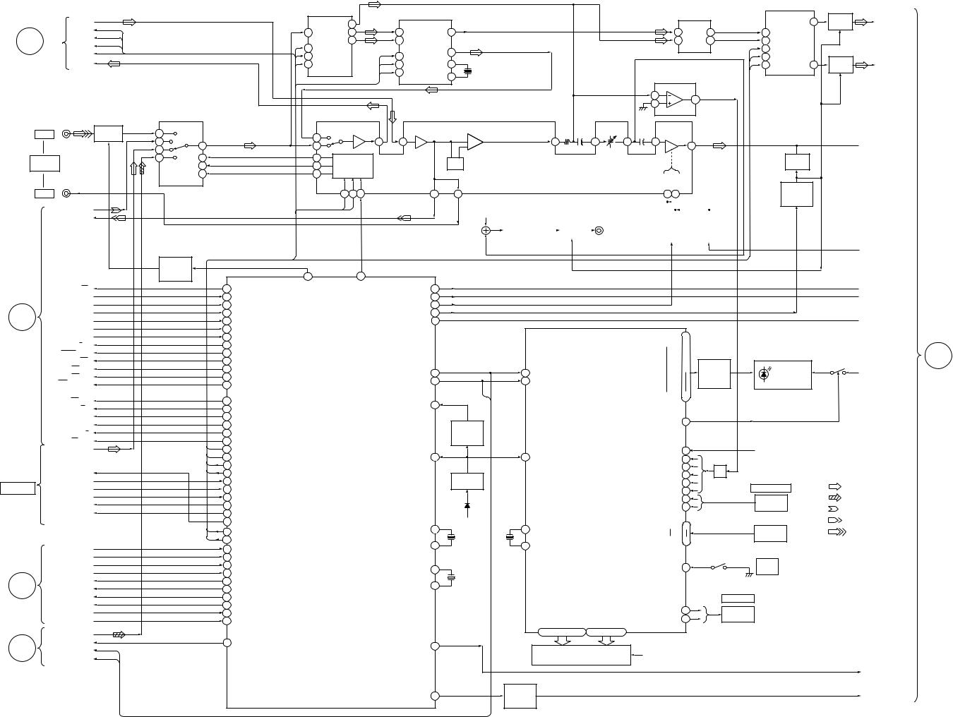
HCD-V909AV
— MAIN SECTION — |
|
|
|
|
|
|
|
|
|
|
|
|
|
|
|
|
|
|
|
|
|
|
|
|
DOLBY PRO LOGIC |
|
|
|
DELAY |
|
|
||||
|
|
|
|
|
|
|
|
IC601 |
|
|
CENTER |
|
|
|
|||
KEY CON |
|
|
|
|
|
|
|
|
|
|
IC602 |
|
|
||||
L IN |
|
|
|
|
|
|
|
|
|
|
|
|
|
|
|||
SECTION |
3 |
|
|
|
|
|
|
C-OUT |
34 |
|
REAR |
|
|
|
|
|
|
A |
DATA |
|
|
|
|
9 |
L-IN |
S-OUT |
35 |
|
|
10 |
S-IN |
S-OUT |
13 |
|
|
4 |
|
|
|
|
|
|
|
||||||||||
CLK |
|
|
|
|
|
|
L-OUT |
37 |
|
|
8 |
L-IN |
|
|
|
||
5 |
|
|
|
3 |
|
|
|
|
|
|
FRONT |
||||||
LATCH |
|
|
|
41 |
DATA |
|
|
|
FRONT |
|
|
L-MIX |
|
||||
6 |
|
|
|
|
|
|
|
|
16 |
||||||||
|
K CON |
|
|
|
4 |
42 CLK |
|
|
|
3 |
3 |
DATA |
OUT |
|
|||
(Page 18) |
|
|
|
|
|
|
|
|
|||||||||
L OUT |
|
|
|
|
2 |
40 EN |
|
|
|
4 |
2 |
CLK |
XTAL |
23 |
|
||
|
|
|
|
|
|
|
|
|
|
|
|
2 |
4 |
EN |
XTAL |
24 |
X601 |
|
|
|
|
|
|
|
|
|
|
|
|
|
|
|
8MHz |
||
|
|
|
|
|
|
|
|
|
|
|
|
|
|
|
FRONT |
|
|
|
|
|
|
INPUT SELECT |
|
|
|
|
|
|
|
|
|
|
|
|
|
|
|
|
|
IC102 |
|
|
|
|
|
|
|
|
|
|
|
|
|
IN L |
MUTE |
V |
1 |
|
|
|
|
|
|
|
|
|
|
|
|
|
|
Q121 |
TC |
|
|
|
|
69 |
|
|
|
|
|
|
|
|
|
||
|
2 |
|
|
|
|
|
|
|
65 |
64 |
|
|
|
||||
|
|
ST |
|
3 |
|
|
71 |
|
|
|
|
|
|
||||
|
|
4 |
|
|
|
|
|
|
|
|
|
|
|
|
|||
|
|
CD |
|
|
|
|
|
|
|
|
|
|
|
|
|
|
|
VIDEO/MD |
|
5 |
A |
10 |
|
|
28 |
|
|
|
|
|
|
|
|
|
|
J101 |
|
|
|
|
MICON |
|
|
|
|
EQ |
|
||||||
|
|
B |
9 |
|
|
29 |
|
|
|
|
|
|
|||||
(AUDIO) |
|
|
|
|
|
|
|
|
|
|
|||||||
|
|
|
|
|
INTERFACE |
|
|
|
|
|
|||||||
|
|
|
|
INH |
6 |
|
|
30 |
|
|
2A |
|
|
||||
|
|
|
|
|
|
|
|
|
|
|
|
|
|
||||
|
|
|
|
|
|
|
|
|
32 33 34 |
|
|
REC |
|
|
|||
OUT L |
|
|
|
|
|
|
|
|
|
|
62 |
61 |
|
||||
|
PB L |
|
|
|
|
|
|
|
4 |
3 |
LATCH |
|
|
|
|
|
R ch |
|
|
|
|
|
|
|
|
|
|
|
|
|
|
|
|||
|
|
|
|
|
|
|
|
|
|
|
|
|
|
|
|
|
|
|
REC L |
|
|
|
|
|
|
|
|
|
|
|
|
|
|
|
|
MUTE |
|
|
CONTROL |
|
|
Q123,124 |
54 |
3 |
|
RELAY REC/PB |
|
96 |
RELAY |
INPUT CHANGE |
427 LAT |
POWER |
98 |
|
A SHUT |
|
26 |
A SHUT |
|
|
D.OUT ON/OFF |
36 |
E |
B SHUT |
|
27 |
B SHUT |
|
|
DBFB H/L |
2 |
B HALF |
|
28 |
B HALF |
|
|
TA MUTE |
1 |
|
|
|
|
|
|||||
|
A HALF |
|
97 |
A HALF |
|
|
R RELAY |
7 |
|
A PLAY |
|
94 |
A PLAY SW |
|
|
|
|
DECK |
B PLAY |
|
95 |
B PLAY SW |
|
|
|
|
SECTION |
PB A / B |
|
87 |
PB A/B |
|
|
|
|
(Page 24) |
NORM/HIGH |
|
88 |
EQ H//N |
|
|
|
|
|
BIAS ON/OFF |
|
89 |
BIAS |
|
|
|
|
|
RM ON/OFF |
|
90 |
REC MUTE |
|
|
IIC DATA |
55 |
|
NR ON/OFF |
|
91 |
NR ON/OFF |
|
|
||
|
|
|
|
IIC CLK |
56 |
|||
|
REC/PB PASS |
|
92 |
R/P PASS |
|
|
||
|
|
|
|
|
|
|||
|
LM ON/OFF |
|
93 |
TC MUTE |
|
|
RESET |
15 |
|
CAP M H/L |
|
82 |
CAP H/N |
|
|
||
|
|
|
|
|
|
|||
|
A TRG |
|
83 |
A TRG |
|
|
|
|
|
B TRG |
|
84 |
B TRG |
|
|
|
RESET |
|
TRIG H/L |
|
85 |
TRG LOW |
|
|
|
SWITCH |
|
CAP M ON/OFF |
1 |
86 |
CAP M ON/OFF |
|
|
|
Q951 |
|
ST L |
41 |
VOL LAT |
|
|
|
|
|
|
2 |
|
|
|
|
|||
|
|
42 |
PL LAT |
|
|
AC CUT |
20 |
|
|
|
3 |
|
|
||||
|
|
44 |
COM DOUT |
MASTER CONTROL |
|
|
|
|
|
|
4 |
|
|
|
|||
FM/AM |
COM DIN |
45 |
COM CLK |
IC701 |
|
|
|
|
|
|
|
RESET |
|||||
TUNER PACK |
COM DATA |
|
66 |
ST DIN |
|
|
|
|
ENCAPSLATED |
STEREO |
|
70 |
STEREO |
|
|
|
IC951 |
COMPONENT |
|
|
|
|
|
|||
TUNED |
|
69 |
TUNED |
|
|
|
|
|
|
|
|
|
|
|
|||
|
ST CE |
|
68 |
ST CE |
|
|
|
D951 |
|
MUTE |
|
72 |
ST MUTE |
|
|
|
|
|
|
5 |
67 |
ST DOUT |
|
|
|
+5V |
|
|
4 |
K CON LAT |
|
|
X1 |
11 |
|
|
|
6 |
|
|
|
X701 |
||
|
|
5 |
K CON ON |
|
|
|
||
|
|
|
|
|
5MHz |
|||
|
|
|
|
|
X2 |
|||
|
OPEN |
|
81 |
OUT OPEN |
|
|
10 |
|
|
|
|
|
|
|
|||
|
ENC-1 |
|
80 |
ENC-1 |
|
|
|
|
|
ENC-2 |
|
79 |
ENC-2 |
|
|
XT1 |
14 |
|
ENC-3 |
|
78 |
ENC-3 |
|
|
||
C |
|
|
|
|
X702 |
|||
LOAD IN |
|
64 |
LOAD IN |
|
|
|
32.768KHz |
|
LOAD OUT |
|
63 |
LOAD OUT |
|
|
XT2 |
13 |
|
|
|
|
|
|||||
|
|
|
|
|
|
|||
|
TBL. L |
|
60 |
TBL L |
|
|
|
|
CD |
TBL. R |
|
61 |
TBL R |
|
|
|
|
SECTION |
DISC SENS |
|
75 |
DISC SENS |
|
|
|
|
(Page 20) |
T. SENS |
|
76 |
T SENS |
|
|
|
|
D |
L CH |
|
|
|
XRST |
57 XRST |
CD POWER |
46 |
|
IIC-DATA |
|
|||
|
|
|||
|
|
|
|
|
|
IIC-CLK |
|
|
|
VIDEO |
|
|
|
|
SECTION |
|
|
|
|
(Page 22) |
|
|
|
|
|
|
|
STK MUTE |
100 |
09 |
|
|
|
|
|
IC603 |
|
REAR |
|
|
3 |
1 |
|
5 |
AMP |
|
7 |
||
CENTER |
|
|
AMP |
|
|
IC861 |
|
|
6 |
7 |
|
5 |
||
|
|
|
|
|
|
FRONT |
45 |
+ |
44 |
43 |
+ |
42 |
|
|
|
38 |
|
EQUALIZER / VOLUME |
|
|
BB22 |
BB12 |
|
|
|
||||||||
|
|
|
|
IC201 |
|
|
|
|
|
|||||||
|
|
|
|
|
|
|
|
|
|
|
|
|
|
|||
|
|
|
|
|
|
|
|
|
40 41 |
|
|
|
|
|||
|
|
|
|
|
|
|
J102 |
|
|
|
|
|
|
|
|
|
|
|
|
|
|
|
|
|
|
|
|
|
|
|
|
||
|
|
|
|
|
|
|
|
|
|
|
|
|
|
|
||
SUPER WOOFER |
|
|
|
|
|
SUPER |
|
DBFB |
|
DBFB |
||||||
|
|
MUTE |
|
|
|
|
||||||||||
|
|
|
|
|
SWITCH |
|
SWITCH |
|||||||||
AMP |
|
|
|
|
|
|
|
|||||||||
|
|
|
Q130 |
|
|
WOOFER |
|
|
||||||||
IC105 |
|
|
|
|
|
|
Q201 |
|
Q202 |
|||||||
|
|
|
|
|
|
|
|
|
||||||||
|
|
|
|
|
|
|
|
|
|
|
|
|
|
|
|
|
|
|
|
|
LED1 |
3 |
|
|
|
|
|
10 |
|
|
|
|
|
|
|
|
|
|
|
|
|
|
• |
|
|
|
|
|
|
15 |
|
|
|
|
|
|
• |
|
|
|
|
|
|
16 |
|
|
|
|
|
|
• |
LED |
|
28 |
DATA |
|
|
18 |
|
|
|
|
|
SWITCH |
||
|
27 |
CLOCK |
|
|
|
|
|
|
|
|
|
||
|
|
|
|
LED16 |
23 |
|
|
|
|
|
LED SELECT |
29 |
|
|
|
DISPLAY CONTROL |
SIRCS |
39 |
|
|
|
14 |
RESET |
IC601 |
|
||
|
SPEANA 1 |
42 |
|
|||
|
|
|
||||
|
|
|
|
|
||
|
|
|
|
SPEANA 2 |
43 |
D/A |
|
|
|
|
SPEANA 3 |
44 |
|
|
|
|
|
|
||
|
|
|
|
SPEANA 4 |
45 |
|
|
|
|
|
L+R |
46 |
|
|
|
|
|
JOG-A |
26 |
|
|
|
|
|
JOG-B |
41 |
|
|
12 |
X-OUT |
|
KEY 5 |
37 |
|
|
|
|
|
|
||
X601 |
13 X-IN |
|
KEY 1 |
33 |
|
|
|
|
|
|
|||
8MHz |
|
|
|
|
|
|
|
|
|
|
DOOR SW |
38 |
|
|
|
|
|
|
|
S602 |
|
|
|
|
|
|
VOLUME |
|
|
|
|
VOL-A |
24 |
ROTARY |
|
|
SEG-1–SEG-35 |
GR-1–GR-16 |
VOL-B |
40 |
ENCODER |
|
|
|
|
|
||
|
|
67 – 100 • 1 |
51 – 66 |
|
|
|
|
|
FL601 |
|
VF |
|
|
|
|
FLUORESCENT INDICATOR TUBE |
|
|
||
|
|
|
|
|
||
|
MUTE |
|
|
|
|
|
|
SWITCH |
|
|
|
|
|
|
Q912 |
|
|
|
|
|
|
|
VOLUME |
|
|
||
|
|
IC604 |
|
|
|
|
|
|
|
|
MUTE |
REAR |
|
|
|
|
OUT 2 |
REAR |
||
|
|
|
Q602 |
|||
|
|
|
|
|
||
|
3 |
IN |
|
|
|
|
4 |
14 |
IN |
|
|
|
|
8 |
CLK |
|
|
|
||
3 |
|
|
|
|||
9 |
DATA |
|
|
CENTER |
||
1 |
|
MUTE |
||||
10 |
LATCH |
OUT 15 |
CENTER |
|||
|
Q601 |
|||||
|
|
|
|
|
||
 FRONT
FRONT
MUTE
Q254
MUTE
SWITCH
Q120
DBFB
 POWER ON/OFF
 DOUT ON/OFF
 R RELAY
Q601-603
PANEL LED |
D+5V |
|
REMOTE |
|
CONTROL |
|
RECEIVER |
|
IC602 |
• R CH: Same as L ch |
|
|
S601 |
• SIGNAL PATH |
|
=AMS + |
: FM |
ROTARY |
: CD |
ENCODER |
: PB |
|
|
|
: REC |
KEY |
: VIDEO |
MATRIX |
|
S681 |
|
6 |
|
OPEN |
|
CD POWER
STK MUTE
F
POWER
SECTION
(Page 27)
— 25 — |
— 26 — |
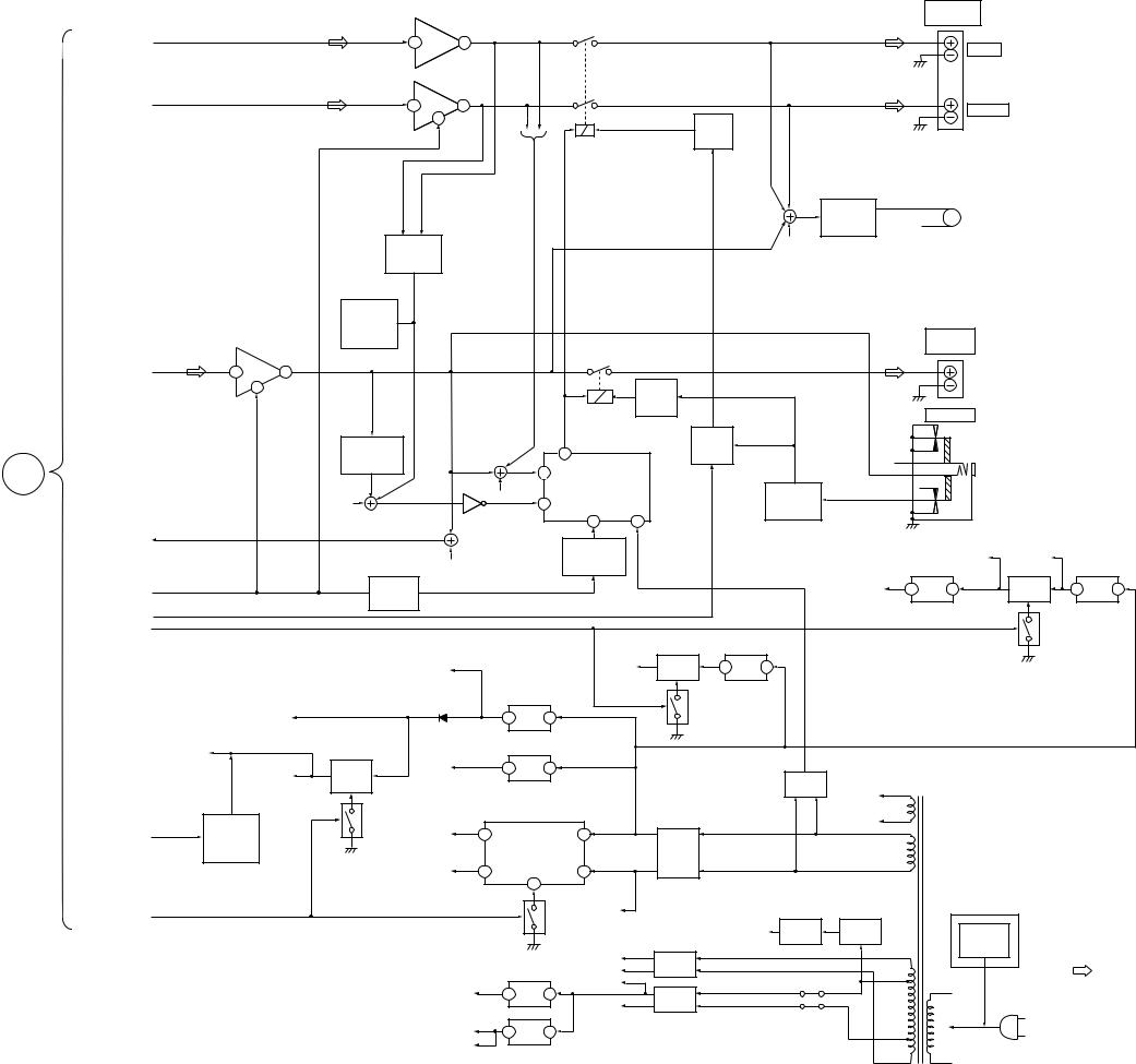
HCD-V909AV
— POWER SECTION —
|
|
|
|
|
|
|
|
|
|
|
|
|
|
|
|
|
|
TM402 |
|
|
|
|
|
|
|
|
POWER AMP |
|
|
|
|
|
|
|
|
|
|
|
|
SURROUND |
|
|
|
||
|
|
|
|
|
|
|
|
|
|
|
|
|
|
|
|
SPEAKER |
|
|
|
|||
|
|
|
|
IC601 |
|
|
|
|
|
|
|
|
|
|
|
|
|
|
|
|
||
|
|
|
REAR |
|
|
|
RY401 |
|
|
|
|
|
|
REAR |
|
|
|
|
|
|||
|
|
|
|
|
|
|
|
|
|
|
|
|
|
|
|
|
|
|||||
REAR |
|
|
1 |
10 |
|
|
|
|
–1 |
|
|
|
|
|
|
|
|
|
|
|
|
|
|
|
|
|
|
|
|
|
|
|
|
|
|
|
|
|
REAR |
|
|
|
|||
|
|
|
|
|
|
|
|
|
|
|
|
|
|
|
|
|
|
|
|
|
|
|
|
|
|
|
|
|
|
|
|
–2 |
|
|
|
|
|
|
CENTER |
|
|
|
|
|
|
CENTER |
|
|
18 |
13 |
|
|
|
|
|
|
|
|
|
|
|
|
|
CENTER |
|
|
|
|
|
|
|
|
|
|
|
|
|
|
|
|
|
|
|
|
|
|
|
||||
|
|
|
CENTER |
6 |
|
|
|
|
|
|
|
|
RELAY |
|
|
|
|
|
|
|
|
|
|
|
|
|
|
|
|
|
|
|
|
|
|
|
|
|
|
|
|
|
|||
|
|
|
|
|
|
|
|
|
|
|
|
|
DRIVE |
|
|
|
|
|
|
|
|
|
|
|
|
|
|
|
|
|
|
|
|
|
|
Q404 |
|
|
|
|
|
|
|
|
|
|
|
|
|
|
|
|
|
|
|
|
|
|
|
|
|
FAN MOTOR |
|
M |
M901 |
|
|
|
|
|
|
|
|
|
|
|
|
|
|
|
|
|
|
|
DRIVER |
UNREG |
FAN |
|
|
|
|
|
|
|
|
|
|
|
|
|
|
|
|
|
|
|
|
Q961, 962 |
|
MOTOR |
|
|
|
|
|
|
|
OVER LOAD |
|
|
|
|
|
|
|
|
|
|
Rch |
|
–12V |
|
|
|
|
|
|
|
|
|
|
|
|
|
|
|
|
|
|
|
|
|
|
|
|
|
|
|||
|
|
|
DET |
|
|
|
|
|
|
|
|
|
|
|
|
|
|
|
|
|
|
|
|
|
|
Q601,651 |
|
|
|
|
|
|
|
|
|
|
|
|
|
|
|
|
|
|
|
|
|
|
THERMAL |
|
|
|
|
|
|
|
|
|
|
|
|
|
|
|
|
|
|
|
|
|
|
DET |
|
|
|
|
|
|
|
|
|
|
|
|
|
|
TM401 |
|
|
|
|
|
POWER AMP |
|
Q670,671 |
|
|
|
|
|
|
|
|
|
|
|
|
|
|
|
|
|
|
|
|
|
|
|
|
|
|
|
|
|
|
|
|
|
|
|
FRONT |
|
|
|
|
||
|
IC201 |
|
THP670 |
|
|
|
|
|
|
|
|
|
|
|
|
|
|
|
|
|
|
|
|
|
|
|
|
|
|
|
|
|
|
|
|
|
|
|
SPEAKER |
|
|
|
|||
|
|
|
|
|
|
|
|
|
|
|
|
|
|
|
|
|
|
|
|
|
||
FRONT |
1 |
10 |
|
|
|
|
|
|
RY402 |
–1 |
|
|
|
|
|
|
FRONT |
|
|
|
|
|
|
|
|
|
|
|
|
|
|
|
|
|
|
|
|
|
|
|
|
||||
|
|
|
|
|
|
|
|
|
|
|
|
|
|
|
|
|
|
|
|
|||
FRONT |
6 |
|
|
|
|
|
|
|
|
|
RELAY |
|
|
|
|
|
|
|
|
|
|
|
|
|
|
|
|
|
|
|
|
|
|
DRIVE |
|
|
|
|
|
|
J760 |
|
|
|
|
|
|
|
|
|
|
|
|
|
|
|
Q403 |
|
|
|
|
|
|
|
|
|
|
|
|
|
|
|
|
|
|
|
|
|
|
|
|
|
|
|
|
PHONES |
|
|
|
||
|
|
|
|
|
|
|
|
|
|
|
|
|
|
|
|
|
|
|
|
|
||
|
|
|
OVER LOAD |
|
|
|
|
|
|
|
|
|
RELAY |
|
|
|
|
|
|
|
|
|
|
|
|
|
|
|
|
6 |
|
|
|
|
CONTROL |
|
|
|
|
|
|
|
|
||
F |
|
|
DET |
|
|
|
|
|
|
|
|
Q402 |
|
|
Rch |
|
|
|
|
|
||
|
|
Q201 |
|
|
|
2 |
|
|
|
|
|
|
|
|
|
|
|
|
|
|||
|
|
|
|
|
|
PROTECTOR |
|
|
|
|
|
|
|
|
|
|
|
|
||||
|
|
|
|
|
|
|
|
|
|
|
HP / SP |
|
|
|
|
|
|
|
||||
|
|
|
|
|
|
Rch |
|
|
IC301 |
|
|
|
|
|
|
|
|
|
|
|
|
|
MAIN |
|
|
Rch |
|
|
|
1 |
|
|
|
|
|
|
|
SWITCHING |
|
|
|
|
|
|
|
SECTION |
|
|
|
Q323 |
|
|
|
7 |
|
4 |
|
|
|
Q401,405 |
|
|
|
|
|
|
|
|
|
|
|
|
|
|
|
|
|
|
|
|
|
|
|
|
|
|
|||||
(Page 26) |
|
|
|
|
|
|
|
|
|
|
|
|
|
|
|
|
|
|
||||
|
|
|
|
|
|
|
|
|
|
|
|
|
|
|
|
|
|
|
|
|
|
|
DBFB |
|
|
|
|
|
|
|
|
PROTECT |
|
|
|
|
|
|
|
|
|
|
|
|
|
|
|
|
|
|
|
|
|
|
|
|
|
|
|
|
|
|
|
D+5V |
D+5V |
|
|
|
|
|
|
|
|
|
|
|
|
SWITCH |
|
|
|
|
|
|
|
+3.3V REG |
|
+5V REG |
|||
|
|
|
|
Rch |
|
|
|
|
Q301 |
|
|
|
|
|
|
|
(SW) |
(UNSW) |
|
|||
|
|
|
|
|
|
|
|
|
|
|
|
|
|
|
|
IC801 |
|
IC9001 |
||||
|
|
|
|
|
|
|
|
|
|
|
|
|
|
|
|
|
|
|
|
|
||
STK MUTE |
|
|
MUTE |
|
|
|
|
|
|
|
|
|
|
|
|
D+3.3V |
2 |
1 |
|
+5V SW |
3 |
1 |
|
|
SWITCH |
|
|
|
|
|
|
|
|
|
|
|
|
|
Q9001 |
||||||
|
|
|
|
|
|
|
|
|
|
|
|
|
|
|
|
|
|
|
|
|||
|
|
|
Q331 |
|
|
|
|
|
|
|
|
|
|
|
|
|
|
|
|
|
|
|
R RELAY |
|
|
|
|
|
|
|
|
|
|
|
|
|
|
|
|
|
|
|
|
|
|
CD POWER |
|
|
|
|
|
|
|
|
|
|
|
|
|
+5V REG |
|
|
|
|
|
Q9002 |
|
|
|
|
|
|
|
|
|
|
|
|
|
|
|
|
|
|
|
|
|
|
|
|
|
|
|
|
|
|
|
|
|
|
|
|
|
|
|
IC9002 |
|
|
|
|
|
|
|
|
|
|
|
|
+5V |
|
|
|
|
|
A+5V |
+5V SW |
3 |
1 |
|
|
|
|
|
|
|
|
|
|
|
|
|
|
|
|
|
|
(SW) |
Q9003 |
|
|
|
|
|
|
|
|
|
|||
|
|
|
|
|
|
|
|
|
|
|
|
|
|
|
|
|
|
|
|
|||
|
|
|
|
|
|
|
+5V REG |
|
|
|
|
|
|
|
|
|
|
|
|
|
|
|
|
|
|
|
D905 |
|
|
IC902 |
|
|
|
|
Q9004 |
|
|
|
|
|
|
|
|
|
|
|
D5V |
|
|
|
3 |
|
1 |
|
|
|
|
|
|
|
|
|
|
|
|
|||
|
|
|
|
|
|
|
|
|
|
|
|
|
|
|
|
|
|
|
|
|||
|
SWITCHED |
|
|
|
|
|
|
|
|
|
|
|
|
|
|
|
|
|
|
|||
|
|
|
|
|
|
|
|
|
|
|
|
|
|
|
|
|
|
|
|
|
||
|
|
|
|
|
|
|
+7V REG |
|
|
|
|
|
|
|
|
|
|
|
|
|
|
|
OPT 5V |
|
|
|
|
|
|
IC903 |
|
|
|
|
|
|
|
|
|
|
|
|
|
|
|
|
|
|
|
|
|
|
|
|
|
|
|
|
|
|
|
|
|
|
|
|
|
|
|
AU/D5V SW |
+5V REG |
D7V |
|
3 |
|
1 |
|
|
|
|
|
|
|
|
T501 |
|
|
|
|
||
|
|
|
|
|
|
|
|
|
|
|
|
RECT |
|
POWER |
|
|
|
|
||||
|
Q906 |
|
|
|
|
|
|
|
|
|
|
|
|
|
|
|
|
|||||
|
|
|
|
|
|
|
|
|
|
|
|
|
|
D302,303 |
|
TRANSFORMER |
|
|
|
|
||
|
|
|
|
|
|
|
|
|
|
|
|
|
|
|
VF |
|
|
|
|
|||
|
|
|
|
|
|
+7V, –7V REG |
|
|
|
|
|
|
|
|
|
|
|
|
|
|||
|
|
|
|
|
|
|
|
|
|
|
|
|
|
|
|
|
|
|
|
|||
|
DOUT |
|
Q907 |
|
|
|
IC901 |
|
|
|
|
|
|
|
|
VF |
|
|
|
|
|
|
|
|
|
|
|
|
|
|
|
|
|
|
|
|
|
|
|
|
|
|
|||
DOUT ON/OFF |
+B |
|
|
A+7.5V |
1 |
+7.5 |
|
VCC |
2 |
|
|
|
|
|
|
|
|
|
|
|
|
|
SWITCH |
|
|
|
|
|
|
|
|
|
RECT |
|
|
|
|
|
|
|
|
|
|
|
|
|
|
|
|
|
|
|
|
|
|
|
|
|
|
|
|
|
|
|
|
|
||
|
Q841, 842 |
|
|
|
|
|
|
|
|
|
|
|
|
|
|
|
|
|
|
|
|
|
|
|
|
|
|
|
|
|
|
|
D901 |
|
|
|
|
|
|
|
|
|
|
|
|
|
|
|
|
|
|
|
|
|
|
|
|
|
|
|
|
|
|
|
|
|
|
|
|
|
|
|
A–7.5V |
10 –7.5 |
EN |
VEE |
9 |
|
|
|
|
|
|
|
|
|
|
|
|
|
|
|
|
|
|
|
|
|
4 |
|
|
|
|
|
|
|
|
|
|
|
|
|
|
|
|
|
|
|
|
|
|
|
|
UNREG |
|
|
|
|
|
|
|
|
E,SP,IA,CH |
|
|
|
|
POWER ON/OFF |
|
|
|
|
|
|
|
Q901 |
–12V |
|
|
|
|
|
VF REG |
RECT |
|
|
|
|
|
|
|
|
|
|
|
|
|
|
|
|
|
|
|
|
VFDP |
|
|
VOLTAGE |
|
• R CH : Same as L ch |
|||
|
|
|
|
|
|
|
|
|
|
|
|
|
|
Q941 |
D104,105 |
|
|
|
||||
|
|
|
|
|
|
|
|
|
|
|
|
|
|
|
|
|
SELECTOR |
|
||||
|
|
|
|
|
|
|
+12V REG |
|
POWER B+ |
RECT |
|
|
|
|
|
|
|
S501 |
|
• SIGNAL PATH |
||
|
|
|
|
|
|
|
|
|
|
|
|
|
|
|
|
|
|
: FM |
||||
|
|
|
|
|
|
|
|
POWER B– |
D101 |
|
|
|
|
|
|
|
|
|
|
|||
|
|
|
|
|
|
|
IC904 |
|
|
|
|
|
|
|
|
|
|
|
||||
|
|
|
|
|
|
|
|
|
SURR B+ |
|
|
|
|
|
|
|
|
|
|
• Abbreviation |
||
|
|
|
|
+12V |
|
3 |
|
1 |
|
|
RECT |
|
|
|
|
|
|
|
|
|
||
|
|
|
|
|
|
|
|
|
|
|
|
|
|
|
|
|
SP : Singapore model. |
|||||
|
|
|
|
|
|
|
|
|
SURR B– |
D102 |
|
|
|
|
|
|
|
|
|
|||
|
|
|
|
ST 10V |
|
3 |
|
1 |
|
|
|
|
|
|
|
|
|
|
|
AC |
IA |
: Indonesian model. |
|
|
|
|
|
|
|
|
|
|
|
|
|
|
|
|
|
IN |
CH : Chinese model. |
||||
|
|
|
|
PRO-LOG 10V |
|
|
+10V REG |
|
|
|
|
|
|
|
|
|
|
|
|
|
||
09 |
|
|
|
|
|
|
|
|
|
|
|
|
|
|
|
|
|
|
|
|
|
|
|
|
|
|
|
|
IC905 |
|
|
|
|
|
|
|
|
|
|
|
|
|
|
|
|
— 27 — |
— 28 — |
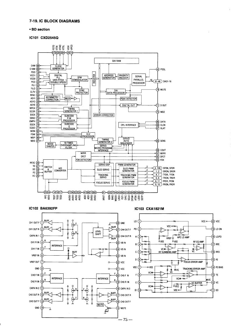
 Loading...