


 Loading...
HCD-VX88
SERVICE MANUAL
E Model
Ver 1.1 2001.08
HCD-VX88 is the tuner, tape player, VIDEO CD/ CD player and amplifier section in MHC-VX88.
This stereo system is equipped with the Dolby B- type noise reduction system*.
* Manufactured under license from Dolby Laboratories Licensing Corporation. DOLBY and the double-D symbol ;are trademarks of Dolby Laboratories Licensing Corporation.
|
|
Model Name Using Similar Mechanism |
HCD-VX77 |
|
|
|
|
CD |
CD Mechanism Type |
CDM58-K2BD37A |
|
|
|
|
|
Section |
Base Unit Name |
BU-K2BD37A |
|
|
|
|
|
|
|
Optical Pick-up Name |
KSM-213DAP/Z-NP |
|
|
|
|
TAPE |
Model Name Using Similar Mechanism |
HCD-VX77 |
|
|
|
|
|
Section |
Tape Transport Mechanism Type |
TCM-230AWR11 |
|
|
|
|
|
SPECIFICATIONS
Amplifier section
The following measured at AC 120, 220, 240V 50/60 Hz
DIN power output (rated) 160 + 160 watts
(6 ohms at 1 kHz, DIN) Continuous RMS power output (reference)
200 + 200 watts (6 ohms at 1 kHz, 10% THD)
Inputs
MD/VIDEO (AUDIO) IN: voltage 450 mV/250 mV,
(phono jacks) |
impedance 47 kilohms |
MIC: |
sensitivity 1 mV, |
(phone jack) |
impedance 10 kilohms |
Outputs |
|
VIDEO OUT: |
max. output level 1 Vp-p, |
(Phono jack) |
unbalanced, Sync |
|
negative, load impedance |
|
75 ohms |
S-VIDEO OUT: |
Y: 1 Vp-p, unbalanced |
(4 pin/mini-DIN jack) |
Sync negative |
|
C: 0.286 Vp-p |
|
load impedence 75 ohms |
PHONES: |
accepts headphones of 8 |
(stereo mini jack) |
ohms or more |
FRONT SPEAKER: |
accepts impedance of 6 to |
|
16 ohms |
SATELLITE SPEAKER: |
accepts impedance of 6 to |
|
16 ohms |
VIDEO CD/CD player section
System |
Compact disc and digital |
|
audio system |
Laser |
Semiconductor laser |
|
(λ =780nm) |
|
Emission duration: |
|
continuous |
Laser output |
Max. 44.6 W* |
|
*This output is the value |
|
measured at a distance of |
|
200 mm from the |
|
objective lens surface on |
|
the Optical Pick-up Block |
|
with 7 mm aperture. |
Frequency response |
2 Hz – 20 kHz (± 0.5 dB) |
Wavelength |
780 – 790 nm |
Signal-to-noise ratio |
More than 90 dB |
Dynamic range |
More than 90 dB |
Video color system format |
NTSC, PAL |
|
|
CD OPTICAL DIGITAL OUT |
|
(Square optical connector jack, rear panel) |
|
Wavelength |
660 nm |
Output Level |
–18 dBm |
Tape player section
Recording system |
4-track 2-channel stereo |
Frequency response |
40 – 13,000 Hz (± 3 dB), |
(DOLBY NR OFF) |
using Sony TYPE I |
|
cassette |
|
40 – 14,000 Hz (± 3 dB), |
|
using Sony TYPE II |
|
cassette |
Tuner section
FM stereo, FM/AM superheterodyne tuner
FM tuner section |
|
Tuning range |
87.5 – 108.0 MHz |
Antenna |
FM lead antenna |
Antenna terminals |
75 ohm unbalanced |
Intermediate frequency |
10.7 MHz |
AM tuner section |
|
Tuning range |
|
Middle Eastern models: |
531 – 1,602 kHz |
|
(with the interval set at 9 |
|
kHz) |
Other models: |
531 – 1,602 kHz |
|
(with the interval set at 9 |
|
kHz) |
|
530 – 1,710 kHz |
|
(with the interval set at 10 |
|
kHz) |
Antenna |
AM loop antenna |
Antenna terminals |
External antenna terminal |
Intermediate frequency |
450 kHz |
— Continued on next page —
|
COMPACT DISC DECK RECEIVER |
9-929-218-12 |
Sony Corporation |
2001H0500-1 |
Home Audio Company |
C 2001.8 |
Shinagawa Tec Service Manual Production Group |
1
General
Power requirements |
|
Thailand models: |
220 V AC, 50/60 Hz |
Other models: |
120 V, 220 V or 230 - 240 |
|
V AC, 50/60 Hz |
|
Adjustable with voltage |
|
selector |
Power consumption |
250 watts |
Dimensions (w/h/d) |
Approx. 280 x 360 x 425 |
|
mm (11 x 143/16 x 1611/16 |
|
in.) |
Mass: |
Approx. 11 kg |
|
(24 lb. 5 oz) |
Design and specifications are subject to change without notice.
TABLE OF CONTENTS
1.SERVICE NOTES ···························································· 4
2.GENERAL ·········································································· 5
3.DISASSEMBLY ································································ 7
4.TEST MODE ···································································· 12
5.MECHANICAL ADJUSTMENTS ····························· 17
6.ELECTRICAL ADJUSTMENTS ······························· 17
7.DIAGRAMS
7-1. Circuit Boards Location ··················································· 23
7-2. Block Diagrams ································································ 25 7-3. Printed Wiring Board – BD Section – ······························ 28 7-4. Schematic Diagram – BD Section – ································· 29 7-5. Printed Wiring Board – VIDEO Section – ······················· 30 7-6. Schematic Diagram – VIDEO (1/3) Section – ················· 31 7-7. Schematic Diagram – VIDEO (2/3) Section – ················· 32 7-8. Schematic Diagram – VIDEO (3/3) Section – ················· 33 7-9. Printed Wiring Board – MAIN Section – ························· 34 7-10. Schematic Diagram – MAIN (1/3) Section – ··················· 35 7-11. Schematic Diagram – MAIN (2/3) Section – ··················· 36 7-12. Schematic Diagram – MAIN (3/3) Section – ··················· 37 7-13. Printed Wiring Board – POWER AMP Section – ············ 38 7-14. Schematic Diagram – POWER AMP Section – ··············· 39 7-15. Printed Wiring Boards – PANEL Section – ······················ 40 7-16. Schematic Diagram – PANEL Section – ·························· 41 7-17. Printed Wiring Boards – LEAF SW Section – ················· 42 7-18. Schematic Diagram – LEAF SW Section – ····················· 43 7-19. Printed Wiring Boards – DRIVER Section – ··················· 44 7-20. Schematic Diagram – DRIVER Section – ······················· 45 7-21. Printed Wiring Board – TRANS Section – ······················· 46 7-22. Schematic Diagram – TRANS Section – ························· 47 7-23. IC Pin Function Description ············································· 48 7-24. IC Block Diagrams ··························································· 57
8.EXPLODED VIEWS ······················································ 62
9.ELECTRICAL PARTS LIST ······································· 68
SAFETY-RELATED COMPONENT WARNING!!
COMPONENTS IDENTIFIED BY MARK 0 OR DOTTED LINE WITH MARK 0 ON THE SCHEMATIC DIAGRAMS
AND IN THE PARTS LIST ARE CRITICAL TO SAFE OPERATION. REPLACE THESE COMPONENTS WITH SONY PARTS WHOSE PART NUMBERS APPEAR AS SHOWN IN THIS MANUAL OR IN SUPPLEMENTS PUBLISHED BY SONY.
2
NOTES ON HANDLING THE OPTICAL PICK-UP BLOCK OR BASE UNIT
The laser diode in the optical pick-up block may suffer electrostatic break-down because of the potential difference generated by the charged electrostatic load, etc. on clothing and the human body.
During repair, pay attention to electrostatic break-down and also use the procedure in the printed matter which is included in the repair parts.
The flexible board is easily damaged and should be handled with care.
NOTES ON LASER DIODE EMISSION CHECK
The laser beam on this model is concentrated so as to be focused on the disc reflective surface by the objective lens in the optical pickup block. Therefore, when checking the laser diode emission, observe from more than 30 cm away from the objective lens.
Laser component in this product is capable of emitting radiation exceeding the limit for Class 1.
This appliance is classified as a CLASS 1 LASER product. The CLASS 1 LASER PRODUCT MARKING is located on the rear exterior.
CAUTION
Use of controls or adjustments or performance of procedures other than those specified herein may result in hazardous radiation exposure.
Notes on chip component replacement
•Never reuse a disconnected chip component.
•Notice that the minus side of a tantalum capacitor may be damaged by heat.
Flexible Circuit Board Repairing
•Keep the temperature of soldering iron around 270˚C during repairing.
•Do not touch the soldering iron on the same conductor of the circuit board (within 3 times).
•Be careful not to apply force on the conductor when soldering or unsoldering.
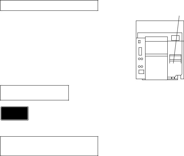
MODEL IDENTIFICATION
— BACK PANEL —
PART No.
|
|
|
|
|
|
|
|
MODEL |
PART No. |
|
|
|
|
|
|
EXCEPT IA model |
4-225-040-7s |
|
|
|
|
|
|
IA model |
4-227-061-2s |
|
|
|
|
|
|
•Abbreviation
IA : Indonesian
3
SECTION 1
SERVICE NOTES
Note for installing the panel board
2 Panel board
Hot melt
 : melted-connection point
Screw hole
1 Cut the nine melted-connection points with cutting pliers.
Attach the panel board with six screws (+BVTP 2.6 × 8 )
after the board is removed once.
Do not tighten the screws excessively.
SELF-DIAGNOSIS
This model has the self-diagnosis function for the VIDEO and AUDIO decoder sections. Connecting to the LED between TP522 and TP523 on the VIDEO BOARD.
Immediately after the power on, the self-diagnosis function searches each operation of IC’s around the CD mechanism control microcomputer (IC502). and TP5
The results can be checked by LED of the VIDEO board.
|
|
Oscilloscope (Waveform) |
|
Symptom |
[VIDEO BOARD] (SIDE A) |
|
||||||||||||||||||
|
|
|
|
|
|
|
|
|
||||||||||||||||
|
|
|
|
|
|
|
|
|
|
|
|
|
|
|
|
|
|
|
|
|
|
|
|
|
|
|
|
|
|
|
|
|
|
|
|
|
|
|
|
H |
|
|
TP523 |
|
TP522 |
|
|||
|
|
|
|
|
|
|
|
|
|
|
|
|
|
|
|
|
|
|||||||
|
|
|
|
|
|
|
|
|
|
|
|
|
|
|
|
|
|
|
|
|
||||
|
|
|
|
|
|
|
|
|
|
|
|
|
|
|
L |
|
No error |
|
|
|
|
|
|
|
|
|
|
|
|
|
|
|
|
|
|
|
|
|
|
|
|
|
|
|
|
|
|||
|
|
|
|
|
|
|
|
|
|
|
|
|
|
|
|
|
LED |
|
||||||
|
|
|
|
|
|
Light |
|
|
|
|||||||||||||||
|
|
|
|
|
|
|
|
|
|
100 |
91 |
|||||||||||||
|
|
|
|
|
|
|
|
|
|
|
|
|
|
|
|
|
|
|
|
|
||||
|
|
|
|
|
|
|
|
|
|
|
|
|
|
|
|
|
|
|
|
|
1 |
90 |
||
|
|
|
|
|
|
|
|
|
|
|
|
|
|
|
H |
|
MPEG decoder (IC505) |
|
|
|
|
IC505 |
|
|
|
|
|
|
|
|
|
|
|
|
|
|
|
|
|
|
|
|
|
|
32 |
65 |
|||
|
|
|
|
|
|
|
|
|
|
|
|
|
|
|
L |
|
error |
|
|
|||||
|
|
|
|
|
|
|
|
|
|
|
|
|
|
|
|
|
|
33 |
64 |
|||||
|
|
|
|
|
2 time blinking |
|
|
|
|
|
|
|
|
|||||||||||
|
|
|
|
|
|
|
|
|
|
|
|
|
|
|
|
|
|
|
|
|
|
|
|
|
|
|
|
|
|
|
|
|
|
|
|
|
|
|
|
|
|
H |
MPEG decoder (IC505) |
|
|
|
|
|
|
|
|
|
|
|
|
|
|
|
|
|
|
|
|
|
|
|
|
|
|
|
|
|
||
|
|
|
|
|
|
|
|
|
|
|
|
|
|
|
|
|
|
|
|
|
|
|
|
|
|
|
|
|
|
|
|
|
|
|
|
|
|
|
|
|
|
L |
or |
|
|
|
|
|
|
|
|
|
|
|
|
3 time blinking |
DRAM (IC507) error |
|
|
|
|
|
|
|||||||||||
|
|
|
|
|
|
|
|
|
|
|
|
|
||||||||||||
|
|
|
|
|
|
|
|
|
|
|
|
|
|
|
|
|
|
|
|
|
|
|
|
|
4
SECTION 2 GENERAL
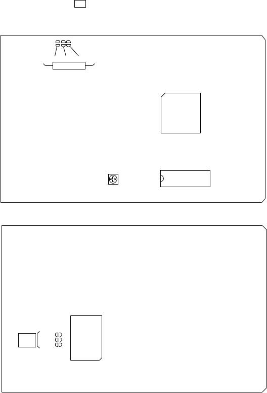
LOCATION OF CONTROLS
• Front view
1 |
2 3 4 5678 |
|
wswdwfwgwh |
9 |
|
0 |
||
wj |
||
qa |
||
wk |
||
qs |
||
wl |
||
qd |
||
e; |
||
qf |
||
ea |
||
qg |
||
es |
||
qh |
||
ed |
||
qj |
||
ef |
||
|
||
eg |
qkql |
|
eh |
||
w; |
||
ej |
||
wa |
||
ek |
||
|
||
el |
|
r;rars rdrf rg rh
1DISC SKIP button
2DISC 1 button and indicator
3DISC 2 button and indicator
4DISC 3 button and indicator
5Z OPEN/CLOSE button
6PREV button
7NEXT button
8RETURN button
9CD disc tray
0Fluorescent indicator tube
qa EDIT, TUNER MEMORY button
qs PLAY MODE, STEREO/MONO button qd REPEAT, DOLBY NR button
qf DIRECTION button
qg CINEMA SPACE button qh VOLUME knob
qj Shuttle knob qk x button
ql hH button w; PHONES jack wa Tape deck-B
ws TAPE A/B button wd CD button
wf Function indicator
wg TUNER/BAND button wh MD (VIDEO) button
wj ?/1 button and indicator wk DISPLAY button
wl SPECTRUM button e; EQ EDIT button ea GROOVE button
es ECHO LEVEL knob ed MIC LEVEL knob ef MIC2 jack
eg MIC1 jack
eh g, G, f, Fbutton and indicator ej PICTURE EFFECT button
ek V-GROOVE button and indicator el Tape deck-A
r; – . button ra Xbutton
rs > + button
rd KARAOKE PON button rf CD SYNC HI-DUB button
rg REC PAUSE/START button and indicator rh ENTER button
5
Step 3: Setting the time
You must set the time before using the timer functions.
O
2,4 |
|
nN X |
|
. > m M x |
1 |
||
|
N X |
x |
|
|
|
|
3,5 |
|
v |
|
|
|
b |
B |
|
|
V |
|
|
1 Press CLOCK/TIMER SET.
The hour indication flashes.
2 Press . or > repeatedly to set the hour.
continued
This section is extracted from instruction manual.
Step 3: Setting the time (continued)
3 Press ENTER.
The minute indication flashes.
4 Press .or > repeatedly to set the minute.
5 Press ENTER.
The clock starts working.
Tip
If you’ve made a mistake, start over from step 1.
To change the time
The previous explanation shows you how to set the time while the power is off. To change the time while the power is on, do the following:
1 Press CLOCK/TIMER SET.
2 Press .or > repeatedly to select SET CLOCK.
3 Press ENTER.
4 Perform steps 2 through 5 above.
Note
The clock settings are canceled when you disconnect the power cord or if a power failure occurs.
9 10
6
SECTION 3
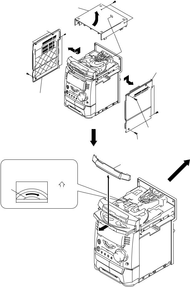
DISASSEMBLY
Note : Follow the disassembly procedure in the numerical order given.
COVER (TOP)
0 cover (TOP)
5 two screws (case3 TP2) 

 7 two screws (BVTP 3 × 8)
6screw
(case3 TP2) 
8 side panel L
 9 two screws (BVTP 3 × 12)
4 side panel R
3 two screws  (BVTP 3 × 10)
1 two screws (case3 TP2)
2 screw
(case 3 TP2)
LOADING PANEL ASS’Y
CD mechanism deck (CDM58-K2BD37A) |
3 loading panel ass’y |
1 Turn the pulley (S) in the direction of the arrow. |
|
Front panel side
pulley (S)
bottom view
2 Pull out the disc tray 
7

FRONT PANEL SECTION, CD MECHANISM DECK (CDM58-K2BD37A)
qa CD mechanism deck |
7 two screws |
(BVTP 3 × 10) |
|
(CDM58-K2BD37A) |
|
8 |
|
|
|
|
9 wire (flat type) (13 core) |
|
|
(CN201) |
4 screw |
|
|
(BVTP 3 × 10) |
|
5 connector |
|
|
|
1 wire (flat type) (17 core) |
(CN401) |
|
|
||
(CN304) |
|
0 connector |
|
|
(CN202) |
4 screw |
|
|
(BVTP 3 × |
10) |
|
2 two connectors |
BASE UNIT (BU-K2BD37A) |
|
(CN 1, 2) |
||
(Page 11) |
||
|
||
6 front panel section |
DRIVER/MOTOR/SENSOR/ |
|
VIDEO BOARDS |
||
|
||
|
(Page 11) |
3three screws (BVTP 3 × 8)
TAPE MECHANISM DECK (TCM-230AWR11)
3 screw
(BVTP 2.6 × 8)
4 bracket (heat cam L)
5 five screws |
|
1 screw |
|
|
(BVTP 2.6 × |
8) |
× 8) |
||
(BVTP 2.6 |
||||
|
|
2 bracket (heat cam R)
LEAF SW/HEAD (A)/HEAD (B) BOARDS (Page 10)
6 tape mechanism deck (TCM-230AWR11)
8

PANEL BOARD
8 three claws
6 two knobs (MIC)
2two screws (BVTP2.6 × 8)
5 spring FR
qs panel board
4 FR knob
qa three claws
3 bracket (FR)
1 vol knob
q; five claws
7 two screws (BVTP2.6 × 8)
9 CD switch board
 : melted-connection point
q; Cut the nine melted-connection points with cutting pliers.
Note: When attaching the panel board, refer to "Service Notes" on page 4.
POWER TRANSFORMER (T971), TRANS BOARD
7Remove six teen solders
of power transformer (T971).
8 TRANS board
4 connector (CN977)
5two screws (BVTP 4 × 8)
6power transformer (T971)
|
3 back panel |
4 connector |
|
(CN975) |
1 six screws |
|
|
|
(BVTP 3 × 10) |
5 two screw |
|
(BVTP 4 × 8) |
|
 1 two screws (BVTP 3 × 10)
2 connector
(CN891)
9
MAIN/POWER AMP BOARDS
2 two connectors (CN901, 902)
3 MAIN board
LEAF SW/HEAD (A)/HEAD (B) BOARDS
3 five claws
plunger (PM1001)
6 HEAD (A) board 

5 ground point screw (PTT 2 × 4)
7 two screws |
8 heat sink |
(BVTP 3 × 8) |
|
5three screws (BVTP 3 × 8)
6 POWER AMP board
4two screws (BVTP 3 × 16)
1two screws (BVTP 3 × 8)
1 Remove two solders of plunger (PM1001) leads.
2 Remove four solders of  capstan/reel motor (M901) lead.
1 Remove two solders of plunger (PM1002) leads.
4 LEAF SW board
plunger (PM1002)
8 HEAD (B) board
7ground point screw (PTT 2 × 4)
10
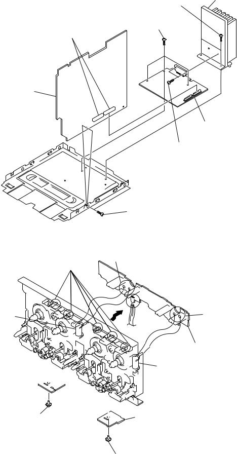
BASE UNIT (BU-K2BD37A)
3
5 base unit 4 two insulators (BU-K2BD37A)
4 two insulators
1 wire (flat type) (23 core)  (CN101)
2 four screws (PTPWH M2.6)
DRIVER/MOTOR/SENSOR/VIDEO BOARDS
0 screw
(PTPWH 2.6 × 8)
9 MOTOR board |
6 two screws |
|
(BVTP 2.6 × 8) |
||
|
4 wire (flat type) (8 core) |
|
|
(CN721) |
|
7 |
|
|
qa tray |
|
|
qd SENSOR board |
5 Remove two solders of turn motor (M721). |
|
8 connector (CN722) |
||
3 DRIVER board |
||
qs screw (BVTP 2.6 × 8) |
||
|
1 connector (CN701)
2 screw
(BVTP 3 × 10)
qg VIDEO board
qf two screws (BVTP 2.6 × 8) 

11

SECTION 4 TEST MODE
[MC Cold Reset]
•The cold reset clears all data including preset data stored in the RAM to initial conditions. Execute this mode when returning the set to the customer.
Procedure:
1. Press three buttons x , ENTER , and ?/1 simulta-neously.
2.The fluorescent indicator tube displays “COLD RESET” and the set is reset.
[CD Ship Mode]
• This mode moves the pickup to the position durable to vibration. Use this mode when returning the set to the customer after repair.
Procedure:
1. |
Press |
?/1 |
button to turn the set ON. |
||
2. |
Press |
|
button and |
?/1 |
button simultaneously. |
CD |
|||||
|
|
|
|
|
|
3.After the "STANDBY" display blinks six times, a message “LOCK” is displayed on the fluorescent indicator tube, and the CD ship mode is set.
[MC Hot Reset]
•This mode resets the set with the preset data kept stored in the memory. The hot reset mode functions same as if the power cord is plugged in and out.
Procedure:
1.Press three buttons x , ENTER , and DISC 1 simultaneously.
2.The fluorescent indicator tube becomes blank instantaneously, and the set is reset.
[CD Service Mode]
• This mode can run the CD sled motor freely. Use this mode, for instance, when cleaning the pickup.
Procedure:
1.Press ?/1 button to turn the set ON.
2.Select the function “CD”.
3.Press three buttons x , ENTER , and OPEN/CLOSE simultaneously.
4.The CD service mode is selected.
5.With the CD in stop status, turn the shuttle knob clockwise to move the pickup to outside track, or turn the shuttle knob counter-clockwise to inside track.
6.To exit from this mode, perform as follows:
1)Move the pickup to the most inside track.
2)Press three buttons in the same manner as step 2.
Note: • Always move the pickup to most inside track when exiting from this mode. Otherwise, a disc will not be unloaded.
•Do not run the sled motor excessively, otherwise the gear can be chipped.
[VACS ON/OFF Mode]
•This mode is used to switch ON and OFF the VACS (Variable Attenuation Control System).
Procedure:
Press the ENTER and SPECTRUM buttons simultaneously. The message “VACS OFF” or “VACS ON” appears.
[Change-over of MW Tuner Step between 9 kHz and 10 kHz]
•A step of MW channels can be changed over between 9 kHz and 10 kHz.
Procedure:
1.Press ?/1 button to turn the set ON.
2.Select the function “TUNER”, and press TUNER/BAND button to select the BAND “AM”.
3.Press ?/1 button to turn the set OFF.
4.Press ENTER and ?/1 buttons simultaneously, and the display of fluorescent indicator tube changes to “AM 9 k STEP” or “AM 10 k STEP”, and thus the channel step is changed over.
[GC Test Mode]
•This mode is used to check the software version, FL tube, LED, keyboard and VACS.
Procedure:
1.Press three buttons x , ENTER , and DISC 2 simultaneously.
2.LEDs and fluorescent indicator tube are all turned on.
3.When you want to enter the software version display mode, press DISC 1 . The model number and destination are displayed.
4.Each time DISC 1 is pressed, the display changes starting from MC version, GC version, VC version, CD version, CM version, ST version, TC version, TA version, TM version and BR version in this order, and returns to the model number and destination display.
5.When DISC 3 is pressed while the version numbers are being displayed except model number and destination, year, month and day of the software creation appear. When DISC 3 is pressed again, the display returns to the software version display. When DISC 1 is pressed while year, month and day of the software creation are being displayed, the year, month and day of creation of the software versions are displayed in the same order of version display.
6.Press DISC 2 button, and the key check mode is activated.
7.In the key check mode, the fluorescent indicator tube displays “KEY0 VOL0 ”. Each time a button is pressed, “KEY” value
increases. However, once a button is pressed, it is no longer taken into account.
“VOL” value increases like 1, 2, 3 ... if rotating VOLUME knob in “+” direction, or it decreases like 0, 9, 8 ... if rotating in “–” direction.
8.Also when DISC 3 is pressed after lighting of all LEDs and FL tubes, value of VACS appears.
9.To exit from this mode, press three buttons in the same manner as step 1, or disconnect the power cord.
12
[MC Test Mode]
• This mode is used to check operations of the respective sections of Amplifier, Tuner, CD and Tape.
Procedure:
1.Press the ?/1 button to turn on the set.
2.Press the three buttons of x , ENTER and DISC 3 simultaneously.
3.A message “TEST MODE” appears on the FL display tube.
4When f (CURSOR UP) button is pressed, GEQ increases to its maximum and a message “GEQ ALL MA” appears.
5.When F(CURSOR DOWN) button is pressed, GEQ decreases to its minimum and a message “GEQ ALL M1” appears.
6.When g (CURSOR LEFT) or G (CURSOR RIGHT) button is pressed, GEQ is set to flat and a message “GEQ FLAT” appears.
7.When the VOLUME control knob is turned clockwise even slightly, the sound volume increases to its maximum and a message “VOLUME MAX” appears for two seconds, then the display returns to the original display.
8.When the VOLUME control knob is turned counter-clockwise even slightly, the sound volume decreases to its minimum and a message “VOLUME MIN” appears for two seconds, then the display returns to the original display.
9.In the test mode, the default-preset channel is called even when the TUNER is selected and an attempt is made to call the preset channel that has been stored in memory, by operating the Shuttle knob. (It means that the memory is cleared.)
10.When CD is selected and the EDIT button is pressed, the disc that is being chucked at this moment becomes the default setting. It means that the default disc only is accessed when any other discs are selected even though the display indication changes accordingly. At the same time, the DISC SKIP EXCHANGE and OPEN/CLOSE cannot be accepted. (It means that the tray motor and the turntable motor are disabled of their operation.)
11.When a tape is inserted in Deck B and recording is started, the input source function selects VIDEO automatically.
12.When x button is pressed to stop recording, the Tape (Deck) B is selected and tape is rewound using the Shuttle knob, tape is rewound, tape is stops at around the record-starting position and playback of the recorded portion of the tape is started. If PAUSE is inserted even once during recording, tape is rewound to the position around the PAUSE position and is played back.
13.When the CD SYNC HI-DUB Button is press during playback of Deck B, either normal speed or high speed can be selected by this button.
14.Select the desired loop by pressing the PLAY MODE button. Insert a test tape AMS-110A or AMS-RO to Deck A.
15.Press the SPECTRUM button to enter the AMS test mode.
16.After a tape is rewound first, the FF AMS is checked, and the mechanism is shut off after detecting the AMS signal twice.
17.Then the REW AMS is checked and the mechanism is shut off after detecting the AMS signal twice.
18.When the check is complete, a message of either OK or NG appears.
19.When you want to exit this mode, press the ?/1 button twice. The cold reset is enforced at the same time.
13
[Aging Mode]
This mode can be used for operation check of CD section and tape deck section.
•If an error occurred:
The aging operation stops and display status.
•If no error occurs:
The aging operation continues repeatedly.
1. Operating method of Aging Mode
Turn on the main power and select “CD” of the function.
1)Set a disc in DISC1 tray. Select CONTINUE ALL DISCS (press the PLAY MODE button), and REPEAT OFF (press the REPEAT button).
2)Load the tapes recording use into the decks A and B respectively.
3)Press three buttons x , ENTER , and DISC SKIP/EX-CHANGE simultaneously.
4)Aging operations of CD and tape are started at the same time.
5)To exit the aging mode, perform [MC Cold Reset].
3. |
Aging Mode in CD section |
|
|
1) |
Display state |
Display |
|
• |
No error occurs |
|
|
AGING[*][*][*][*]
Note:
[*][*][*][*] : Number of aging operations
Error display
E ** s ## $$ %% |
|
|
|
||||||
12 3 4 5 |
|
|
|
|
|
|
|
||
|
|
|
|
|
|
|
|||
1 ** |
The error No. 00 indicates the newest error. As the error No. increases, it means the older error. |
||||||||
|
When you want to retrieve the error history, press the |
PLAY MODE |
|
button in the case of mechanism error. |
|||||
|
|
|
|
|
|
||||
|
Or press the |
REPEAT |
button in the case of NO DISC error. |
|
|
|
|||
|
|
|
|
|
|
|
|
|
|
2 s |
M: Mechanism error |
|
D: No disc error |
||||||
|
|
|
|
|
|
|
|
||
3 ## |
Don’t care |
|
01: FOCUS ERROR |
||||||
|
|
|
|
|
|
|
|
02: GFS ERROR |
|
|
|
|
|
|
|
|
|
03: SETUP ERROR |
|
|
|
|
|
|
|
|
|
||
4 $$ |
High order digits only |
|
01: NO DISC judgment without chucking retry |
||||||
|
D: Stopped during closing due to problems other than mechanism. |
|
02: NO DISC judgment after chucking retry |
||||||
|
E: Stopped during opening due to problems other than mechanism. |
|
|
|
|||||
|
C: Stopped during chucking due to problems other than mechanism. |
|
|
|
|||||
|
F: Stopped during EX-opening due to problems other than mechanism. |
|
|
||||||
|
|
|
|
|
|
|
|
||
5 %% |
Emergency related errors (High order digits only) |
|
Status at the time of NO DISC judgment |
||||||
|
1: |
Stopped during chuck-up |
|
(High order digits only) |
|||||
|
2: |
Stopped during chuck-down |
|
1: |
STOP |
||||
|
3: Time out by EX-OPEN |
|
2: |
SETUP |
|||||
|
5: |
Time out by EX-CLOSE |
|
3: |
TOC READ |
||||
|
|
|
|
|
|
|
|
4: |
ACCESS |
|
|
|
|
|
|
|
|
5: |
PLAY BACK |
|
|
|
|
|
|
|
|
6: |
PAUSE |
|
|
|
|
|
|
|
|
7: |
MANUAL SEARCH (PLAY) |
|
|
|
|
|
|
|
|
8: |
MANUAL SEARCH (PAUSE) |
|
|
|
|
|
|
|
|
|
|
• When the buttons x , ENTER and DISC 1 are pressed simultaneously, number of time of the mechanism error and the NO DISC error can be checked.
Display: EMC**EDC**
• When aging operation is complete, be sure to perform the MC Cold Reset to reset the error history.
14

2) Operation during aging mode
In the aging mode, the program is executed in the following sequence.
(1)The disc tray opens and closes.
(2)The mechanism accesses DISC 2 and makes an attempt to read TOC. However, since there are no discs, a message “CD2 NO DISC” appears.
(3)The mechanism accesses DISC 3 and a message “CD3 NO DISC” appears.
(4)The disc tray turns to select a disc1.
(5)A disc is chucked.
(6)TOC of disc is read.
(7)The pickup accesses to the track 1, and playing 2 seconds.
(8)The pickup accesses to the last track, and playing 2 seconds.
(9)Every time when an aging operation of step 1 to step 8 is complete, the display “AGING[*][*][*][*]” value increases as the number of aging operations is counted up.
(10)Returns to step 1.
3. Aging Mode in Tape Deck section
1) Display state
•No error occurs Display action now
•Error occurred
Display action last time
NO. |
Display action |
Action contents |
Final timing |
1 |
TAPE A AG-1 |
Rewind the TAPE A, B |
The top of tape |
|
|
|
|
2 |
TAPE A AG-2 |
FWD play the TAPE A |
2 minutes playing |
3 |
TAPE A AG-3 |
F.F. the TAPE A |
20 second FF or the end |
|
|
|
of tape |
|
|
|
|
4 |
TAPE A AG-4 |
REV play the TAPE A |
2 minutes playing |
5 |
TAPE A AG-5 |
Rewind the TAPE A |
The top of tape |
|
|
|
|
6 |
TAPE B AG-2 |
FWD play the TAPE B |
2 minutes playing |
|
|
|
|
7 |
TAPE B AG-3 |
F.F. the TAPE B |
20 second FF or the end |
|
|
|
of tape |
|
|
|
|
8 |
TAPE B AG-4 |
REV play the TAPE B |
2 minutes playing |
|
|
|
|
9 |
TAPE B AG-5 |
Rewind the TAPE B |
The top of tape |
|
|
|
|
2) Operation during aging mode
In the aging mode, the program is executed in the following sequence.
(1)Rewind is executed up to the top of tape A and B.
(2)A tape on FWD side is played for 2 minutes.
(3)FF is executed up to either made for 20 second or the end of tape.
(4)A tape is reversed, and the tape on REV side is played for 2 minutes.
(5)Rewind is executed up to the top of tape.
(6)Returns to step 2, and repeat steps from 2 to 5.
[Function Change Mode]
* Select either VIDEO or MD of the external FUNCTION input.
Procedure:
1.Turn on the power.
2.Press the two buttons ENTER and ?/1 at the same time. The main power is turned on and the other function of the previous function is selected and displayed. “MD” or “VIDEO”.
15
VIDEO CD COLOR-BARS MODE
On this mode, the data of the color-bars signal as a picture signal and the 1kHz sine wave signal as a sound signal are output by the CD mechanism control microcomputer (IC502) for video CD signal check. When measurement of the voltage and waveform on the VIDEO board, perform it in this mode.
For reference, the color-bars signal can be observed at J302 (VIDEO OUT) and the sound signal can be observed at J101 (VIDEO/MD (AUDIO) OUT) using an oscilloscope.
1.Connect the lead wire to both ends of the land of SL503 of the VIDEO board.
2.Turn the power on. Press CD button to select CD.
3.After 2 or 3 seconds later, connect the lead wire.
4.After measuring, remove the lead wire connected.
[VIDEO BOARD] (SIDE A)
SL501 SL502 SL503
TEST MODE
IC505
CT503 |
|
|
VIDEO |
IC507 |
|
FREQUENCY |
||
|
[VIDEO BOARD] (SIDE B)
TEST |
SL503 |
IC502 |
|
SL502 |
|||
MODE |
|
||
SL501 |
|
||
|
|
16
SECTION 5
MECHANICAL ADJUSTMENTS
Precaution
1.Clean the following parts with a denatured alcohol-moistened swab:
record/playback heads |
pinch rollers |
erase head |
rubber belts |
capstan |
idlers |
2.Demagnetize the record/playback head with a head demagnetizer.
3.Do not use a magnetized screwdriver for the adjustments.
4.After the adjustments, apply suitable locking compound to the parts adjusted.
5.The adjustments should be performed with the rated power supply voltage unless otherwise noted.
Torque Measurement
Mode |
Torque meter |
Meter reading |
|
|
|
|
|
|
|
3.06 N • m to 6.96 N • m |
|
FWD |
CQ-102C |
31 to 71 g • cm |
|
|
|
(0.43 – 0.98 oz • inch) |
|
|
|
|
|
FWD |
|
0.19 N • m to 0.58 N • m |
|
CQ-102C |
2 to 6 g • cm |
||
back tension |
|||
|
(0.02 – 0.08 oz • inch) |
||
|
|
||
|
|
|
|
|
|
3.06 N • m to 6.96 N • m |
|
REV |
CQ-102RC |
31 to 71 g • cm |
|
|
|
(0.43 – 0.98 oz • inch) |
|
|
|
|
|
REV |
|
0.19 N • m to 0.58 N • m |
|
CQ-102RC |
2 to 6 g • cm |
||
back tension |
|||
|
(0.02 – 0.08 oz • inch) |
||
|
|
||
|
|
|
|
|
|
6.96 N • m to 14.02 N • m |
|
FF/REW |
CQ-201B |
71 to 143 g • cm |
|
|
|
(0.98 – 1.99 oz • inch) |
|
|
|
|
|
|
|
9.80 N • m |
|
FWD tension |
CQ-403A |
100 g or more |
|
|
|
(3.53 oz or more) |
|
|
|
|
|
|
|
9.80 N • m |
|
REV tension |
CQ-403R |
100 g or more |
|
|
|
(3.53 oz or more) |
|
|
|
|
SECTION 6
ELECTRICAL ADJUSTMENTS
DECK SECTION 
 0 dB=0.775 V
1.Demagnetize the record/playback head with a head demagnetizer.
2.Do not use a magnetized screwdriver for the adjustments.
3.After the adjustments, apply suitable locking compound to the parts adjust.
4.The adjustments should be performed with the rated power supply voltage unless otherwise noted.
5.The adjustments should be performed in the order given in this service manual. (As a general rule, playback circuit adjustment should be completed before performing recording circuit adjustment.)
6.The adjustments should be performed for both L-CH and R- CH.
7.Switches and controls should be set as follows unless otherwise specified.
• Test Tape
Tape |
Signal |
Used for |
|
|
|
P-4-A100 |
10 kHz, –10 dB |
Azimuth Adjustment |
|
|
|
WS-48B |
3 kHz, 0 dB |
Tape Speed Adjustment |
|
|
|
P-4-L300 |
315 Hz, 0 dB |
Level Adjustment |
|
|
|
Record/Playback Head Azimuth Adjustment
DECK A 
 DECK B
Note: Perform this adjustments for both decks
Procedure:
1. Mode: Playback
test tape P-4-A100
(10 kHz, –10 dB)
MAIN board CN301
Pin 3 (L-CH)
Pin 1 (R-CH) level meter
set
+
–
MAIN board CN301
Pin 2 (GND)
17

2.Turn the adjustment screw and check output peaks. If the peaks do not match for L-CH and R-CH, turn the adjustment screw so that outputs match within 1dB of peak.
L-CH |
within |
|
|
1dB |
|
|
|
peak |
|
|
within |
Output |
|
|
|
|
|
1dB |
|
level |
|
|
|
R-CH |
|
|
|
peak |
|
|
Screw |
Screw |
|
|
|
position |
L-CH |
R-CH |
position |
|
peak |
peak |
|
3. Mode: Playback
test tape |
|
|
|
|
P-4-A100 |
|
oscilloscope |
||
(10 kHz, –10 dB) |
pin 3 |
|||
L-CH |
|
|
||
|
|
|
||
MAIN |
pin 2 |
|
|
|
L |
V |
H |
||
board |
||||
|
||||
CN301 |
R |
|
|
|
set |
|
|
||
|
|
|
||
R-CH
pin 1
waveform of oscilloscope
in phase 45 ° 90 ° 135 ° 180 °
good wrong
4.After the adjustments, apply suitable locking compound to the pats adjusted.
Adjustment Location: Playback Head (Deck A).
Record/Playback/Erase Head (Deck B).
forward
reverse
Tape Speed Adjustment DECK B
Note: Start the Tape Speed adjustment as below after setting to the test mode.
In the test mode, the tape speed is high during pressing the
CD SYNC HI-DUB button.
Procedure:
1.Turn the power switch on.
2.Press the x button, ENTER button and DISC 3 button simultaneously.
(The “TEST MODE” on the fluorescent indicator tube display while in the test mode.)
To exit from the test mode, press the ?/1 button. Mode: Playback
test tape
WS-48B frequency counter (3 kHz, 0 dB)
set |
+ |
|
– |
||
|
MAIN board
CN301 (Pin 3 : L-CH) (Pin 1 : R-CH)
1.Insert the WS-48B into the deck B.
2.Press the gG button on the deck B.
3.Press the CD SYNC HI-DUB button in playback mode. Then at HIGH speed mode.
4.Adjust RV1001 on the LEAF SW board do that frequency counter reads 6,000 ± 30 Hz.
5.Press the CD SYNC HI-DUB button. Then back to NORMAL speed mode.
6.Adjust RV1002 on the LEAF SW board so that frequency
counter reads 3,000 ± 15 Hz.
Adjustment Location: LEAF SW board
Playback Level Adjustment DECK A 
 DECK B
Procedure:
Mode: Playback
test tape |
|
|
|
P-4-L300 |
|
|
level meter |
(315 Hz, 0 dB) |
|
||
|
|
||
|
set |
+ |
|
|
– |
||
|
|
|
|
|
|
MAIN board |
|
|
|
CN301 (Pin 3 : L-CH) |
|
|
|
|
(Pin 1 : R-CH) |
Deck A is RV302 (L-CH) and RV352 (R-CH), Deck B is RV303 (L-CH) and RV353 (R-CH) so that adjustment within adjustment level as follows.
Adjustment Level:
CN301 PB level: 301.5 to 338.3 mV (–8.2 to –7.2 dB) level difference between the channels: within ±0.5 dB
Adjustment Location: MAIN board
Sample Volue of Wow and Flutter: 0.3% or less W. RMS (WS-48B)
18

REC Bias Adjustment DECK B
Procedure:
INTRODUCTION
When set to the test mode performed in Tape Speed Adjustment, when the tape is rewound after recording, the “REC memory mode” which rewinds only the recorded portion and playback is set.
This “REC memory mode” is convenient for performing this adjustment. During recording, the input signal FUNCTION will automatically switch to VIDEO.
(If do not operation of stopped from recording complete, and rotate of shuttle knob then rewind to recording start position.)
1.Press MD (VIDEO) button to select VIDEO. (This step is not necessary if the above test mode has already been set.)
2.Insert a tape into deck B.
3.After press REC PAUSE/START button, press REC PAUSE/
 START button, then recording start. 4. Mode: Record
MD/VIDEO (AUDIO) IN
1)315 Hz
50 mV (–23.8 dB)
2)10 kHz
AF OSC |
blank tape |
|
|
600 Ω |
CN-123 |
attenuator |
|
|
set |
5. Mode: Playback
recorded |
|
level meter |
portion |
|
|
|
|
|
|
set |
+ |
|
– |
|
|
|
|
|
CN301 (Pin 3 |
: L-CH) |
|
(Pin 1 |
: R-CH) |
6.Confirm playback the signal recorded in step 3 become adjustable level as follows.
If these levels do not adjustable level, adjustment the RV304
(L-CH) and RV354 (R-CH) on the AUDIO board to repeat steps 4 and 5.
Adjustable Level: Playback output of 315 Hz to playback output of 10 kHz: ±1.0 dB
Adjustment Location: MAIN board
REC Level Adjustment DECK B
Procedure:
INTRODUCTION
When set to the test mode performed in Tape Speed Adjustment, when the tape is rewound after recording, the “REC memory mode” which rewinds only the recorded portion and playback is set.
This “REC memory mode” is convenient for performing this adjustment. During recording, the input signal FUNCTION will automatically switch to VIDEO.
(If do not operation of stopped from recording complete, and rotate of shuttle knob then rewind to recording start position.)
1.Press MD (VIDEO) button to select VIDEO. (This step is not necessary if the above test mode has already been set.)
2.Insert a tape into deck B.
3.After press REC PAUSE/START button, press REC PAUSE/
 START button, then recording start.
4. Mode: Record
MD/VIDEO (AUDIO) IN |
|
|
315 Hz, 50 mV (–23.8 dB) |
|
|
AF OSC |
blank tape |
|
600 Ω |
||
CS-123 |
||
attenuator |
|
|
set |
|
5. Mode: Playback
recorded portion
|
level meter |
|
set |
+ |
|
– |
||
|
CN301 (Pin 3 : L-CH)
(Pin 1 : R-CH)
6.Confirm playback the signal recorded in step 3 become adjustable level as follows.
If these levels do not adjustable level, adjustment the RV301
(L-CH) and RV351 (R-CH) on the MAIN board to repeat steps 4 and 5.
Adjustable Level:
CN301 PB level: 47.2 to 53.0 mV (–24.3 to –23.3 dB)
Adjustment Location: MAIN board
[MAIN BOARD] (Component Side)
REC LEVEL (L) PB LEVEL (L)
(A)
CN301
PB LEVEL (R) |
3 |
1 |
RV301 |
|
(A) |
||||
|
|
RV352 |
||
PB LEVEL (R) |
|
|
||
|
|
RV302 |
||
(B) |
|
|
||
|
RV353 |
|||
|
|
|||
RV351 |
|
RV303 |
||
|
|
|
||
REC LEVEL (R) |
PB LEVEL (L) |
|||
|
||||
REC BIAS (L) |
|
(B) |
RV304 |
|
|
|
|
||
REC BIAS (R) |
RV354 |
|
[LEAF SW BOARD] |
TAPE SPEED |
TAPE SPEED |
|
(HIGH) |
(NORMAL) |
||
|
(Conductor Side)
RV1001 
RV1002
19
FM Tuned Level Adjustment
FM RF SSG
75 Ω coaxial
Carrier frequency : 98 MHz
Modulation |
: AUDIO 1 kHz, 75 kHz |
|
deviation (100%) |
Output level |
: 28 dB (at 75 W open) |
set
FM ANTENNA terminal (TM601)
Procedure:
1.Supply a 28 dB 98 MHz signal from the ANTENNA terminal.
2.Tune the set to 98 MHz.
3.Adjust RV611 to the point (moment) when the TUNED indicator on the fluorescent indication tube will change from going off to going on.
Adjustment Location: MAIN board
Null Adjustment
FM RF SSG
75 Ω coaxial
Carrier frequency : 98 MHz
Modulation |
: AUDIO 1 kHz, 75 kHz |
|
deviation (100%) |
Output level |
: 60 dB (at 75 W open) |
set
FM ANTENNA terminal (TM601)
Procedure:
1.Supply a 60 dB 98 MHz signal from the ANTENNA terminal.
2.Tune the set to 98 MHz.
3.Measure voltage between pin wa of IC 601. Adjust T601 until the voltage becomes 0 V.
Adjustment Location: MAIN board
[MAIN BOARD] (Component Side)
NULL
FM TUNED LEVEL
T601
RV611
CN301 |
|
CN304 |
|
|
|
||
3 |
1 |
RV301 |
|
|
|
RV302 |
|
|
|
RV352 |
CN302 |
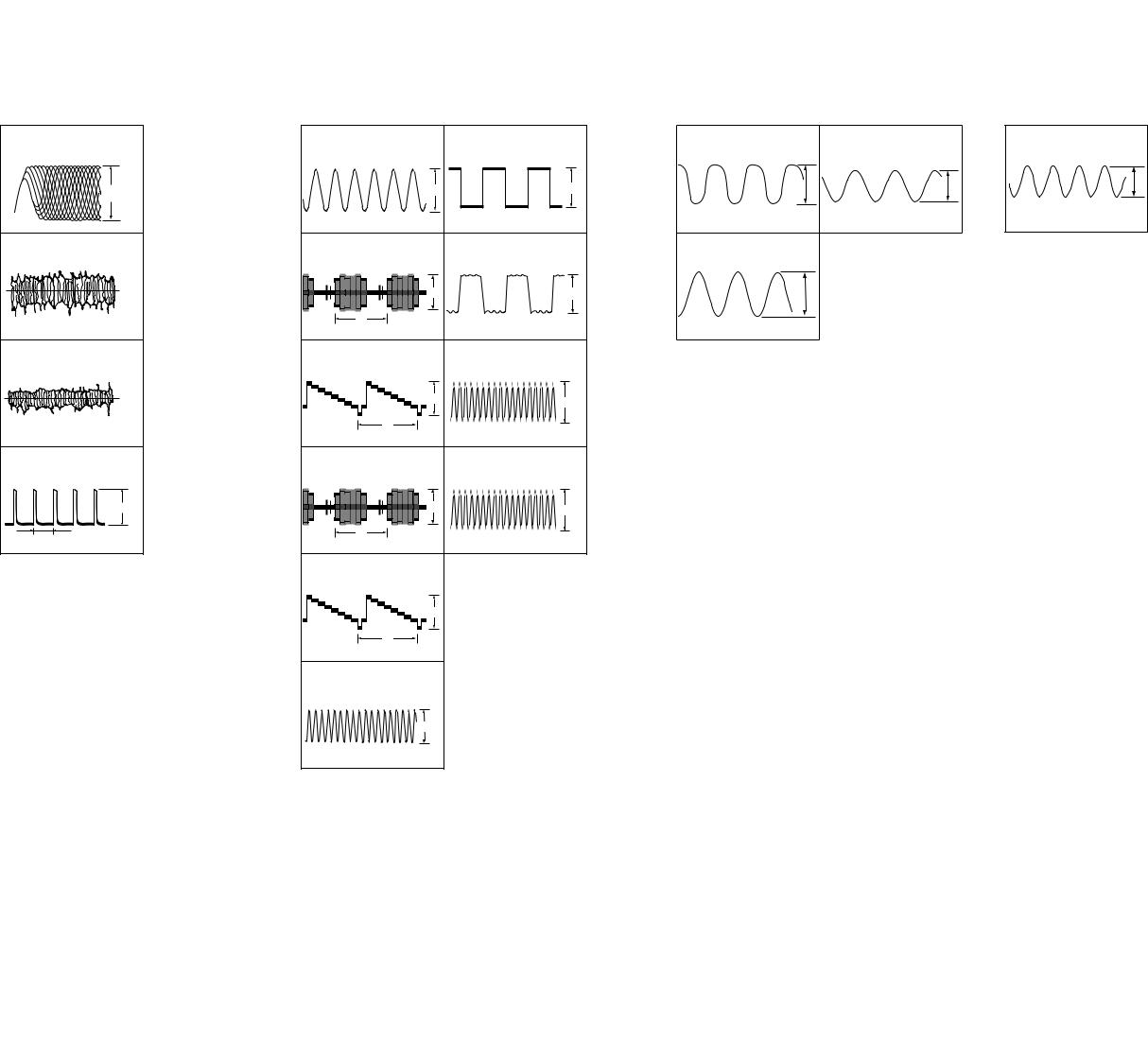
RV353 
RV351 |
RV303 |
|
CN303 |
|
RV304 |
|
RV354 |
CD SECTION
Note :
1.CD Block is basically designed to operate without adjustment. Therefore, check each item in order given.
2.Use YEDS-18 disc (3-702-101-01) unless otherwise indicated.
3. Use an oscilloscope with more than 10MΩ impedance.
4.Clean the object lens by an applicator with neutral detergent when the signal level is low than specified value with the following checks.
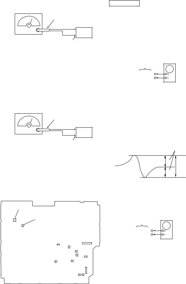
S-Curve Check
oscilloscope
BD board
TP(FEO)
TP(VC)
Procedure :
1.Connect oscilloscope to TP (FEO).
2.Connect between TP (FEI) and TP (VC) by lead wire.
3.Connect between TP (AGCCON) and TP (GND) by lead wire.
4.Turn Power switch on.
5.Load a disc (YEDS-18) and actuate the focus search. (In consequence of open and close the disc tray, actuate the focus search)
6.Confirm that the oscilloscope waveform (S-curve) is symmetrical between A and B. And confirm peak to peak level within 4 ±1 Vp-p.
S-curve waveform
symmetry
A
within 4 ± 1Vp-p
B
7. After check, remove the lead wire connected in step 2 and 3.
Note : • Try to measure several times to make sure than the ratio of A : B or B : A is more than 10 : 7.
•Take sweep time as long as possible and light up the brightness to obtain best waveform.
RF Level Check
oscilloscope
BD board
TP(RF)
TP(VC)
Procedure :
1.Connect oscilloscope to TP (RF).
2.Connect between TP (AGCCON) and TP (GND) by lead wire.
3.Turned Power switch on.
4.Load a disc (YEDS-18) and playback.
5.Confirm that oscilloscope waveform is clear and check RF signal level is correct or not.
6.After check, remove the lead wire connected in step 2.
20
Note: Clear RF signal waveform means that the shape “◊ ” can be clearly distinguished at the center of the waveform.
RF signal waveform
VOLT/DIV : 200mV
TIME/DIV : 500ns
level : 1.45 ± 0.3Vp-p
E-F Balance (1 Track Jump) Check
|
oscilloscope |
BD board |
|
TP (TEO) |
+ |
TP (VC) |
– |
Procedure:
1. Connect oscilloscope to TP (TEO) and TP (VC) board. 2. Turned Power switch on.
3. Load a disc (YEDS-18) and playback the number five track. 4. Press the hH button. (Becomes the 1 track jump mode.) 5. Confirm that the level B and A (DC voltage) on the oscilloscope
waveform.
1 track jump waveform
|
Center of |
|
waveform |
|
B |
0V |
A (DC voltage) |
|
|
level=1.3± 0.6Vp-p |
Symmetry |
Specification level: A x 100=less than ±22% |
|
B |
|
6.After check, remove the lead wire connected in step 1.
RF PLL Free-Run Frequency Check
Procedure :
1.Connect frequency counter to test point (XPCK) with lead wire.
BD board |
frequency counter |
|
|
TP (XPCK) |
+ |
|
– |
2.Turned Power switch on.
3.Put the disc (YEDS-18) in to play the number five track. Confirm that reading on frequency counter is 4.3218MHz.
21

Adjustment Location :
[BD BOARD] (SIDE B)
TP (RF)
TP (VC)
TP (AGCCON) |
TP (FEO) |
||
TP (TEO) |
|||
|
|
||
|
|
TP (FEI) |
|
TP |
IC103 |
TP (XPCK) |
|
(GND) |
|
IC101 |
|
|
|
||
VIDEO SECTION
VIDEO Frequency Adjustment
1.Connect the frequency counter to check point of the VIDEO board.
2.Adjust CT503 of the VIDEO board so that the frequency counter read 27MHz ± 80Hz at STOP condition.
Adjustment Location :
[VIDEO BOARD] – SIDE A –
frequency counter
VIDEO board
TP (27 MHz)
+
–
[VIDEO BOARD] – SIDE B –
SL501 SL502 SL503
TEST MODE
IC505
|
TP |
TEST |
SL503 |
IC502 |
|
SL502 |
|||
(27MHz) |
MODE SL501 |
|
||
CT503 |
|
|
|
|
VIDEO |
|
IC507 |
|
|
FREQUENCY |
TP |
|
|
|
|
(GND) |
|
|
|
22
SECTION 7
DIAGRAMS
THIS NOTE IS COMMON FOR PRINTED WIRING BOARDS AND SCHEMATIC DIAGRAMS. (In addition to this, the necessary note is printed in each block.)
Note on Schematic Diagram:
•All capacitors are in µF unless otherwise noted. pF: µµF 50 WV or less are not indicated except for electrolytics and tantalums.
•All resistors are in Ω and 1/4 W or less unless otherwise specified.
•% : indicates tolerance.
•f : internal component.
•2: nonflammable resistor.
•5: fusible resistor.
•C : panel designation.
Note: The components identified by mark 0or dotted line with mark 0are critical for safety.
Replace only with part number specified.
•U : B+ Line.
•V : B– Line.
•H: adjustment for repair.
•Voltages are taken with a VOM (Input impedance 10 MΩ).
Voltage variations may be noted due to normal production tolerances.
•Waveforms are taken with a oscilloscope.
Voltage variations may be noted due to normal production tolerances.
•Circled numbers refer to waveforms.
•Signal path. F : FM f : AM
E : PB (DECK A) d : PB (DECK B)
G : REC (DECK B)
J : CD (AUDIO) c : digital out o : CD (VIDEO) m : VIDEO (C) n : VIDEO (Y)
•Abbreviation
EA : Saudi Arabia model
Note on Printed Wiring Boards:
•X : parts extracted from the component side.
•Y : parts extracted from the conductor side.
•b: Pattern from the side which enables seeing.
Caution: |
|
|
|
|
|||||||||||
Pattern face side: |
Parts on the pattern face side seen from |
||||||||||||||
(Side B) |
|
|
|
the pattern face are indicated. |
|||||||||||
Parts face side: |
Parts on the parts face side seen from |
||||||||||||||
(Side A) |
|
|
|
the parts face are indicated. |
|||||||||||
|
|||||||||||||||
• Indication of transistor. |
|||||||||||||||
|
|
|
C |
|
|
|
|
||||||||
|
|
|
|
|
|
|
|||||||||
|
|
|
|
|
|
|
|
|
|
|
|
|
|
|
|
|
|
|
Q |
|
|
|
These are omitted. |
||||||||
|
|
|
|
|
|
||||||||||
|
B E |
|
|
|
|
||||||||||
|
|
|
|
|
|
|
|
|
|
Q |
|
|
|
|
|
|
|
|
|
|
|
|
|
|
|
|
|
|
|
||
|
|
|
|
|
|
|
|
|
|
|
|
|
|
||
|
B C |
E |
|
||||||||||||
These are omitted.
7-1. CIRCUIT BOARDS LOCATION
MOTOR board
SENSOR board
TRANS board
CD SWITCH board
PANEL board
LEAF SW board
HEAD (A) board
HEAD (B) board
HCD-VX88
DRIVER board
VIDEO board
BD board
MAIN board
POWER AMP board
23 23
HCD-VX88
Waveforms
– CD SECTION –
1 IC101 t; |
RFAC |
1.3Vp-p |
2 IC101 ra |
TE |
2.5V |
APPROX 500mVp-p |
3 IC101 el |
FE |
2.5V |
APPROX 200mVp-p |
4 IC101 wg |
MDP |
2.6Vp-p |
7.5μsec |
– VIDEO SECTION – |
|
– MAIN BOARD – |
|
|
|
– PANEL BOARD – |
|
1 IC502 qd |
7 IC509 ql |
1 IC401 qa |
|
3 T301 4 |
|
1 IC601 oa |
|
XOUT |
LRCK |
STOP MODE |
|
TAPE B REC MODE |
STOP MODE |
|
|
4Vp-p |
|
4.6Vp-p |
|
|
|
|
|
|
|
32.768kHz |
3.0Vp-p |
80.7kHz |
120Vp-p |
12.5MHz |
4.8Vp-p |
10MHz |
44.1kHz |
|
|
||||
|
|
|
|
|
|
||
2 IC505 ug |
8 IC509 qj |
2 IC401 qd |
|
|
|
|
|
COUT |
BCK |
STOP MODE |
|
|
|
|
|
1Vp-p |
4.8Vp-p |
H |
2.11MHz |
16MHz |
3.4Vp-p |
|
|
|
3 IC505 yl |
|
9 IC504 8 |
YOUT |
|
384FS |
|
|
2Vp-p |
|
|
4.8Vp-p |
|
H |
33.8MHz |
|
|
|
4 IC304 9 |
|
q; IC504 6 |
COUT |
|
27M |
1Vp-p |
3.8Vp-p |
|
H |
27MHz |
5IC304 qg YOUT
2Vp-p
H
6IC509 1 XT1
5.8Vp-p
27MHz
24 24
HCD-VX88
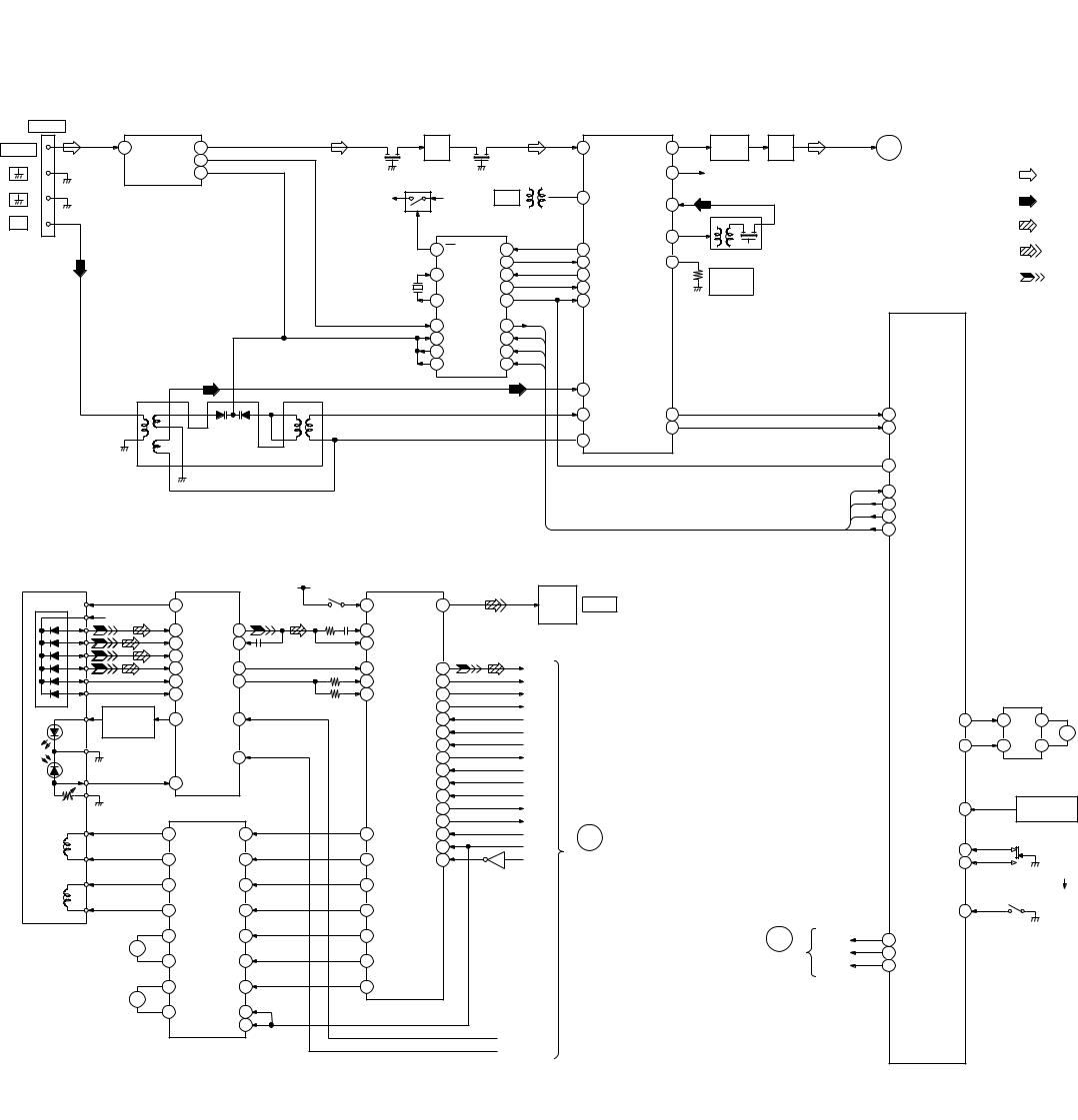
7-2. BLOCK DIAGRAMS
– TUNER/CD SECTION –
|
TM601 |
FE602 |
|
|
|
|
|
|
|
|
AM/FM IF MPX |
|
|
|
|
|
|
|
|
ANTENNA |
FM FRONT-END |
|
|
Q601 |
|
|
|
|
|
|
LPF601 |
|
|
|
|||
|
|
|
|
|
|
|
|
IC601 |
|
|
|
|
|
|||||
FM 75Ω |
8 |
ANT IN IF OUT |
1 |
CF601 |
IF |
|
CF602 |
|
1 |
FM IF |
L OUT |
11 |
BUFFER |
LPF |
L-CH |
A |
• R-CH: Same as L-CH. |
|
|
AMP |
|
|
|
Q611 |
|
• Signal Path |
|||||||||||
|
F OUT |
3 |
|
|
|
|
|
|
|
|
|
|
||||||
|
|
|
|
|
|
|
|
|
|
|
|
|
|
|
MAIN |
|||
|
|
|
|
|
|
|
|
|
|
|
|
|
|
|
|
|||
|
|
VT |
4 |
|
|
|
|
|
|
|
|
R OUT 10 |
R-CH |
|
|
|
||
|
|
B+ SWITCH |
|
|
|
|
|
|
|
|
SECTION |
: FM |
||||||
|
|
|
|
|
|
|
T601 |
|
|
|
|
|
|
|
(Page 27) |
|
||
|
|
|
|
Q602 |
|
|
|
|
5 |
|
|
|
|
|
|
|
||
|
|
|
|
+B |
|
A+12V |
|
|
NULL |
FM DET |
AM IF IN |
18 |
|
|
|
|
: AM |
|
|
|
|
|
|
|
|
|
|
|
|
|
IFT601 |
|
|
|
|
||
|
|
|
|
|
|
|
|
|
|
|
|
|
|
|
|
|
|
|
AM |
|
|
|
|
|
|
PLL |
|
|
|
|
|
|
|
|
|
|
: CD (AUDIO) |
|
|
|
|
|
|
IC651 |
|
|
|
|
AM MIX OUT |
19 |
|
|
|
|
|
|
|
|
|
|
|
|
|
|
|
|
|
|
|
|
|
|
|
||
|
|
|
|
|
10 |
FM |
FM/AM IF |
12 |
9 |
IF OUT |
|
|
|
|
|
|
: DIGITAL OUT |
|
|
|
|
|
|
|
|
|
FM |
7 |
12 AM/FM |
FM SD ADJ |
3 |
RV611 |
|
|
|
|
|
|
|
|
|
X651 |
1 |
XIN |
AM OSC 14 |
24 |
AM OSC OUT |
|
FM TUNED |
|
|
|
: CD (VIDEO) |
|||
|
|
|
|
|
VCO STOP |
2 |
13 |
VCO STOP |
|
LEVEL |
|
|
|
|
||||
|
|
|
|
4.5MHz |
24 |
XOUT |
IF REQ |
8 |
8 |
IF REQ MUTE |
|
|
|
|
SYSTEM CONTROLLER |
|
||
|
|
|
|
|
|
|
|
|
|
|||||||||
|
|
|
|
|
|
|
|
|
|
|
|
|
|
|
|
|
IC401(1/2) |
|
|
|
|
|
|
15 FM OSC |
DO |
6 |
DO |
|
|
|
|
|
|
|
|
||
|
|
|
|
|
DI |
|
|
|
|
|
|
|
|
|||||
|
|
|
|
|
18 |
VT1 IN |
DI |
4 |
|
|
|
|
|
|
|
|
||
|
|
|
|
|
CL |
|
|
|
|
|
|
|
|
|||||
|
|
|
|
|
17 |
VT1 |
|
CL |
5 |
|
|
|
|
|
|
|
|
|
|
|
|
|
|
|
CE |
|
|
|
|
|
|
|
|
||||
|
|
|
|
|
19 |
PD1 |
|
CE |
3 |
|
|
|
|
|
|
|
|
|
|
|
|
|
|
|
|
|
|
|
|
|
|
|
|
||||
RB641 |
|
|
|
|
|
|
|
|
|
|
AM FRONT-END |
|
|
|
|
20 |
AM RF IN |
|
|
|
|
13 |
|
14 |
|
|
|
|
|
|
||
|
|
|
|
|
|
|
|
|
||
1 |
4 |
11 |
15 |
9 |
22 |
AM OSC |
TUNED |
6 |
24 |
TUNED |
|
|
5 |
|
|
||||||
|
|
|
|
|
|
STEREO |
7 |
23 |
STEREO |
|
3 |
|
|
6 |
7 |
|
|
||||
|
|
23 |
V REG |
|
|
|
|
|||
|
|
|
|
|
|
|
|
|
||
2 |
12 |
|
|
|
|
|
|
|
22 |
ST MUTE |
|
|
|
|
|
|
|
|
|
DO |
27 |
ST DIN |
|
DI |
|||
26 |
ST DOUT |
||
CL |
|||
28 |
ST CLK |
||
CE |
|||
25 |
ST CE |
||
|
OPTICAL PICK-UP |
|
|
|
|
|
|
|
|
DIGITAL SERVO, |
|
|
|
|
|
|
|
|
||
BLOCK |
|
|
|
RF AMP |
|
|
A+5V |
DIGITAL SIGNAL PROCESSOR, |
|
|
|
|
|
|
|
||||
|
|
|
|
|
S101 |
D/A CONVERTER |
|
IC201 |
|
|
|
|
|
|
|||||
(KSS-213D/ZN) |
|
|
|
|
|
|
|
|
|
|
|
|
|||||||
|
|
|
IC103 |
|
|
|
(LIMIT) |
|
IC101 |
|
OPTICAL |
|
|
|
|
|
|
||
|
|
|
|
|
|
|
|
|
|
|
|
|
|
|
|
|
|
||
|
|
|
|
|
|
|
|
|
|
|
|
|
OPTICAL |
|
|
|
|
|
|
|
VC |
|
12 |
VC |
|
|
|
|
26 |
SSTP |
D OUT 64 |
DIGITAL |
|
|
|
|
|
||
|
|
+5V |
|
|
|
|
|
|
|
|
|
|
OUT |
|
|
|
|
|
|
|
A |
|
|
|
|
|
|
|
|
|
|
|
|
|
|
|
|
|
|
|
|
5 |
A |
RFO 16 |
|
|
50 |
RFAC |
|
|
|
|
|
|
|
|
|
||
|
B |
|
|
|
|
|
|
|
|
|
|
|
|
||||||
|
|
6 |
B |
RFI 17 |
|
|
43 |
RFDC |
|
|
|
|
|
|
|
|
|
||
|
C |
|
|
|
|
|
|
|
|
|
|
|
|
||||||
|
|
7 |
C |
|
|
|
|
|
|
|
|
|
|
|
|
|
|
|
|
|
D |
|
|
|
|
|
|
|
|
|
|
|
|
|
|
|
|
||
|
|
8 |
D |
FE |
14 |
|
|
39 |
FE |
PCMD |
66 |
A DATA |
|
|
|
|
|
|
|
|
E |
|
|
|
|
|
|
|
|
|
|||||||||
|
|
11 |
E |
TE |
13 |
|
|
41 |
TE |
B CLK |
67 |
B CLK |
|
|
|
|
|
|
|
|
F |
|
|
|
|
|
|
|
|
|
|||||||||
|
|
10 |
F |
|
|
|
|
40 |
SE |
L RCK |
65 |
L RCK |
|
|
|
|
|
|
|
|
|
Q101 |
|
|
|
|
|
|
|
IC701 |
|
|
|||||||
|
|
|
|
|
|
|
|
|
|
C2PO |
14 |
C2PO |
|
|
|
|
|
||
|
LD |
AUTOMATIC |
|
|
|
|
|
|
|
|
|
|
|
|
|
|
|||
|
3 |
LD |
LD ON 22 |
|
|
|
|
DATA |
4 |
DATA |
|
MTR CNT2 44 |
9 |
|
4 |
|
|||
|
|
POWER |
|
|
|
|
|
MOTOR |
M721 |
||||||||||
|
|
|
|
|
|
|
|
|
|
|
|
|
|
|
|
|
|||
|
|
CONTROL |
|
|
|
|
|
|
|
|
XLAT |
5 |
XLT |
|
|
|
M |
(TURN) |
|
|
|
|
|
|
|
|
|
|
|
|
|
|
DRIVE |
||||||
|
GND |
|
|
|
|
|
|
|
|
|
CLOK |
6 |
CLK |
|
MTR CNT1 45 |
7 |
2 |
|
|
|
|
|
|
|
|
|
|
|
|
|
|
|
|||||||
|
|
|
|
|
HOLD SW 21 |
|
|
|
|
SENS |
7 |
SENS |
|
|
|
|
|
|
|
|
PD |
|
|
|
|
|
|
|
|
|
S CLK |
8 |
S CLK |
|
|
|
|
|
|
|
|
4 |
PD |
|
|
|
|
|
|
MUTE |
3 |
MUTE |
|
|
|
|
|
|
|
|
|
|
|
|
|
|
|
|
|
|
|
|
IC711 |
|
|||||
VR |
|
|
|
|
|
|
|
|
|
|
XTSL |
69 |
CTRL1 |
|
|
|
|
|
|
|
|
|
|
|
|
|
|
|
|
|
|
|
TABLE ADDRESS |
|
|||||
|
|
|
|
|
IC102 |
|
|
|
|
|
SCOR |
15 |
SCOR |
|
T SENS 49 |
|
|
||
|
|
|
|
|
|
|
|
|
|
|
|
SENSOR |
|
||||||
|
|
|
MOTOR/COIL DRIVE |
|
|
|
|
SQSO 76 |
SUBQ |
|
|
|
|
||||||
|
|
|
|
|
|
|
|
|
|
|
|
|
|||||||
|
F+ |
|
|
|
|
|
|
|
|
|
|
|
|
|
|
|
|||
|
|
14 VO1 (+) OPIN1 (+) |
2 |
|
33 |
FFDR |
SQCK |
77 |
SQCK |
B |
|
|
|
|
|
||||
FOCUS |
|
|
|
|
|
|
|
|
|||||||||||
|
|
|
|
|
|
|
|
|
|
XRST |
2 |
XRST |
OPEN SW 46 |
|
|
S701 |
|
||
COIL |
F- |
|
|
|
|
|
|
|
|
|
VIDEO |
|
|
|
|||||
|
13 VO1 (–) OPIN1 (–) |
3 |
|
34 |
FRDR |
XTAI |
71 |
MCK |
|
|
|
||||||||
|
|
|
|
|
|
||||||||||||||
|
|
|
|
SECTION |
CLOSE SW 47 |
|
|
(OPEN/CLOSE) |
|||||||||||
|
T+ |
|
12 VO2 (+) OPIN2 (+) |
5 |
|
31 |
TFDR |
|
IC104 |
(Page 26) |
|
|
|
OPEN |
|
||||
|
|
|
|
|
|
|
|
|
|
|
|
||||||||
|
|
|
|
|
|
|
|
|
|
|
|
|
|||||||
TRACKING |
|
|
|
|
|
|
|
|
|
CLOSE |
COIL |
T- |
11 VO2 (–) OPIN2 (–) |
6 |
32 |
TRDR |
|
|
|
BU UP/DOWN SW 48 |
S711 |
|
|
|
|
|||||||
|
|
|
|
|
||||||
05 |
|
|
|
|
|
|
|
|
|
(BU UP/DOWN) |
|
|
|
|
|
|
|
|
|
|
|
|
M102 |
16 VO4 (–) OPIN4 (–) 26 |
30 |
SRDR |
C |
I2C-DATA |
30 |
IIC-DATA |
|
|
|
(SLED) |
M |
|
|
|
VIDEO |
I2C-CLK |
29 |
IIC-CLK |
|
|
|
15 VO4 (+) OPIN4 (+) |
27 |
29 |
SFDR |
|
||||
|
|
SECTION |
XRST |
43 |
XRST |
|
||||
|
|
|
|
|
|
|
||||
|
|
18 VO3 (–) OPIN3 (–) |
23 |
25 |
MDP |
(Page 26) |
|
|
|
|
|
M101 |
|
|
|
|
|
||||
|
M |
|
|
|
|
|
|
|
|
|
|
(SPINDLE) |
|
|
|
|
|
|
|
|
|
|
|
17 VO3 (+) STBY1 |
9 |
|
|
|
|
|
|
|
|
|
STBY2 |
20 |
|
|
|
|
|
|
|
|
|
|
|
|
|
LD ON |
|
|
|
|
|
|
|
|
|
|
LPH |
|
|
|
|
25 25

HCD-VX88
– VIDEO SECTION –
D-RAM
IC507
WE RAS UCAS LCAS |
A0 |
A8 |
DQ1 |
DQ16 |
13 14 28 29 |
16 - 19 |
22 - 26 |
2 - 10 |
31 - 39 |
ROM
IC506
O0 |
|
|
O7 |
A11 |
|
A17 |
|
|
|
||||
13 - 15 |
17 - 21 |
25 4 28 29 3 2 30 |
||||
A0 |
|
A10 |
|
CE |
12 - 5 27 26 23 |
22 |
|||
|
|
|
|
|
38 42 |
40 |
|
|
10 - 29 |
58 - 44 |
37 |
|
|
|
|
|
|
|
|
|
|
|
|
|
|
|
|
|
|
|||
|
|
|
LEVEL SHIFT |
|
MWE RASO |
CAS |
|
|
MD0 |
I |
MD15 |
MA0 I |
MA10 |
MCE |
|
|
|
|
|
|
|
|
|
|
IC304 |
|
|
|
|
|
|
|
|
|
|
|
|
|
|
|
|
|
|
|
|
|
|
|
|
|
|
|
|
|
|
Y/C AMP, |
|
|
|
|
|
|
|
||
|
|
|
IC501 |
|
|
|
|
|
|
|
|
|
|
|
|
|
|
|
IC303 |
|
|
|
|
MIX AMP |
|
|
|
|
|
|
|
|
|
|
|
|
|
|
|
|
|
|
|
|
|
|
|
|
|
|
HUE CONTROL |
|
|
|
|
|
|
|
|
|
|
|
|
|
|
|
ADATA |
1 |
4 |
4 |
CD-DATA |
|
|
|
|
|
|
|
|
Y-OUT |
69 |
|
10 |
VIDEO |
VIDEO |
1 |
|
|
2 |
Y IN |
MIX OUT1 |
12 |
|
|
|
J302 |
|
|
|
|
|
|
|
|
|
|
|
|
|
|
|
|
VIDEO OUT |
|
|||||||||||||||||
|
BCLK |
13 |
10 |
3 |
CD-BCK |
|
|
|
|
|
|
|
|
|
|
|
|
IN |
OUT |
|
|
|
|
|
|
|
|
|
|
|||
|
|
|
|
|
|
|
|
|
|
|
|
|
|
|
|
|
|
|
|
|
|
|
|
|
|
|||||||
|
LRCK |
5 |
8 |
5 |
CD-LRCK |
|
|
|
|
|
|
|
|
|
|
|
5 |
CONTROL |
|
|
|
|
|
|
|
|
|
|
|
|
|
|
|
|
|
|
|
|
|
|
|
|
|
|
|
|
|
|
|
|
|
|
|
|
|
|
|
|
|
|
J301 |
||||
|
|
|
|
|
|
|
|
|
|
|
|
|
|
|
|
|
|
|
|
|
|
|
|
|
Y OUT1 |
15 |
|
|
|
|
||
|
|
|
|
|
|
|
|
|
|
|
|
|
|
|
|
|
|
|
|
|
|
|
|
|
4 |
|
3 |
|
S VIDEO |
|||
|
C2PO |
|
|
6 |
CD-C2PO |
|
|
|
|
|
|
|
|
|
|
|
|
|
IC302 |
|
|
|
|
|
|
|
|
|
||||
|
|
|
|
MPEG VIDEO/AUDIO DECODER, |
|
|
|
|
|
|
|
|
|
|
|
|
|
|
|
|
|
|
|
|
OUT |
|||||||
|
|
|
|
|
|
|
|
|
|
|
|
|
|
Y AMP/PICTURE CORRECTION |
|
|
|
|
|
|
2 |
1 |
|
|
|
|
||||||
|
|
|
|
|
|
|
VIDEO SIGNAL PROCESSOR |
|
|
|
|
|
|
|
|
|
|
|
|
|
|
|
|
|
|
|
|
|
|
|
||
|
|
|
DATAI |
112 |
HD-OUT |
|
|
IC505 |
|
|
|
|
|
C-OUT |
75 |
|
1 |
V IN |
V OUT |
6 |
|
|
7 |
C IN |
|
|
|
|
|
|
|
|
|
|
|
DATAO |
|
|
|
|
|
|
|
|
|
|
|
8 |
TINT |
|
|
|
|
|
|
|
|
|
|
|
|
|
|
||
|
|
|
119 |
HD-IN |
|
|
|
|
|
|
|
|
|
|
|
|
|
|
|
|
|
|
|
|
|
|
|
|
|
|||
|
|
|
CLK1 |
|
|
|
|
|
|
|
|
|
|
|
|
|
|
|
|
|
|
|
|
|
|
|
|
|
|
|
||
|
|
|
117 |
HCK |
|
|
|
|
|
|
|
|
|
|
|
5 |
BGD |
|
|
|
|
1 |
|
C OUT1 |
9 |
|
|
|
|
|
|
|
|
|
|
HRDY |
|
|
|
|
|
|
|
|
|
|
|
|
|
|
|
MUTEA |
|
|
|
|
|
|
|||||||
|
|
|
113 |
HRDY |
|
|
|
|
|
|
|
|
|
|
|
IC301 |
|
|
|
|
|
|
|
|
|
|
|
|||||
|
|
|
INT |
|
|
|
|
|
|
|
|
|
|
|
|
|
|
|
|
|
|
|
|
|
|
|
|
|
|
|||
|
|
|
114 |
HINT |
|
|
|
|
|
|
|
|
|
|
|
|
|
|
|
|
|
8 |
MUTEB |
|
|
|
|
|
|
|
|
|
|
|
|
HSEL |
|
|
|
|
|
|
|
|
DA-DATA |
110 |
|
|
|
|
|
|
|
|
|
|
|
|
|
|
|
||||
|
|
|
121 |
HSEL |
|
|
|
|
|
|
|
|
|
|
|
|
|
|
|
|
|
|
|
|
|
|
|
|
|
|||
|
|
|
RST |
|
|
|
|
|
|
|
|
|
|
|
|
|
|
|
|
|
|
|
|
|
|
|
|
|
||||
|
|
|
60 |
RESET |
|
|
|
|
|
|
|
|
DA-LRCK |
108 |
|
|
|
|
|
|
|
|
|
|
|
|
|
|
|
|
|
|
|
|
|
|
|
|
|
|
|
|
|
|
|
|
|
|
|
|
|
|
|
|
|
|
|
|
|
|
|
||||
|
|
|
INVERTER |
93 |
PGIO2/VSYNC/CSYNC |
|
|
|
|
|
|
|
DA-BCK |
111 |
|
27MHz |
|
|
|
|
|
|
|
|
|
|
|
|
|
|
|
|
|
|
|
|
|
|
|
|
|
|
VCK-IN |
106 |
|
|
|
|
|
|
|
|
|
|
|
|
|
|
|
|
|||||
|
|
|
Q502 |
|
|
|
|
|
|
|
|
|
|
DA-XCLK |
86 |
|
|
|
DIGITAL FILTER & D/A CONVERTER |
|
|
|
|
|
|
|
|
|
|
|
||
|
|
|
|
|
|
|
|
|
|
|
|
|
|
|
|
|
|
|
|
|
|
|
|
|
|
|
|
|||||
|
|
|
INVERTER |
|
|
|
|
|
|
|
|
|
|
|
|
|
|
|
|
IC509 |
|
|
|
|
LOW-PASS FILTER |
|
|
|
|
|
||
|
|
|
101 |
PGIO3/HSYNC |
|
|
|
|
|
|
|
|
|
|
|
|
|
|
|
|
|
|
|
|
|
|
|
|||||
|
|
|
|
|
|
|
|
|
|
|
|
|
|
|
|
|
|
|
|
|
|
IC101 |
|
|
|
|
|
|||||
|
|
|
Q501 |
|
|
|
|
|
|
|
|
|
|
|
|
|
|
|
|
|
|
|
|
|
|
|
|
CD-L |
D |
|
||
|
|
|
|
|
|
|
|
|
|
|
|
|
|
|
|
|
|
|
18 |
|
|
|
|
14 |
3 |
|
1 |
|
||||
|
|
|
|
|
|
|
|
|
|
|
|
|
|
|
|
|
|
|
D/A |
|
|
|
|
|
|
|
|
|||||
|
|
|
|
|
|
|
|
|
|
|
|
|
|
|
|
|
|
|
19 |
PLM |
|
|
|
|
|
|
|
|||||
|
|
|
|
|
|
|
|
|
|
|
|
|
|
|
|
|
|
|
|
|
|
|
|
|
|
|
|
|
||||
|
|
|
|
|
|
|
|
|
|
|
|
|
|
|
|
|
|
|
CONV |
|
|
11 |
R-CH |
|
|
|
|
|
|
|||
|
|
|
|
|
|
|
|
|
|
|
|
|
|
|
|
|
|
|
17 |
|
|
|
|
|
|
|
|
|
MAIN |
|
||
|
|
|
|
|
|
|
|
|
|
|
|
|
|
|
|
|
|
|
|
|
|
|
|
|
|
|
|
|
|
|
|
|
|
|
|
|
|
|
|
|
|
|
|
|
|
|
|
|
|
|
DATAO |
|
|
|
|
|
|
|
|
|
|
|
|
SECTION |
|
|
|
|
|
|
|
|
|
|
|
|
|
|
|
|
|
|
|
9 |
|
CLOCK |
|
|
1 |
|
|
|
|
|
|
(Page 27) |
||
B |
|
|
|
|
|
|
|
|
|
|
|
|
|
|
|
|
|
CLK1 |
|
|
|
|
|
|
|
|
|
|||||
|
|
|
|
|
|
|
|
|
|
|
|
|
|
|
|
|
|
|
|
|
|
|
|
|
|
|
|
|
|
|
||
|
|
|
|
|
|
|
|
|
|
|
|
|
|
|
|
|
|
8 |
MODE |
DIVIDER |
|
|
|
X503 |
|
|
|
|
|
|
|
|
|
|
|
|
|
|
CD MECHANISM CONTROLLER |
|
|
|
|
|
|
|
|
|
|
|
7 |
|
|
|
24 |
27MHz |
|
|
|
|
|
|
|
||
|
|
|
|
|
|
|
|
|
|
|
|
|
|
|
|
|
|
|
|
|
|
|
|
|
|
|
|
|||||
|
|
|
|
|
|
|
IC502 |
|
|
|
|
|
|
|
|
|
|
|
|
|
|
|
|
|
CT503 |
|
|
|
|
|
|
|
CD |
|
|
|
|
|
|
|
|
|
|
|
|
|
|
|
|
|
|
|
|
|
|
|
|
|
|
|
|
|
|
|
|
|
|
|
|
|
|
|
|
|
|
|
|
|
|
|
|
|
|
|
10 |
21 20 |
4 |
|
|
VIDEO |
|
|
|
|
|
|
|
|
SECTION |
|
|
|
|
|
|
RESOLUTION |
3 |
|
|
|
|
|
|
|
|
|
|
|
|
|
|
|
|
|
|
|
|
||||
|
|
|
|
|
|
|
|
|
|
|
|
|
|
|
|
|
RSTB |
|
|
|
|
FREQUENCY |
|
|
|
|
|
|
||||
(Page 25) |
|
|
|
|
|
|
CHROMA LEVEL |
4 |
|
|
|
|
|
|
|
|
|
|
|
|
|
|
|
|
|
|
|
|
|
|||
|
|
|
|
|
|
|
|
|
|
|
|
|
|
|
|
|
|
|
|
|
|
|
|
|
|
|
|
|
|
|||
|
|
|
DATAO |
31 |
DATA1O |
|
BGP |
20 |
|
|
|
|
|
|
|
|
|
|
|
|
|
|
|
|
|
|
|
|
|
|
|
|
|
|
|
DATAI |
|
V. MUTE |
65 |
|
|
|
|
|
|
|
|
|
|
|
|
|
|
|
|
|
|
|
|
|
|
|
|
||
|
|
|
32 |
DATA1I |
|
|
|
|
|
|
|
|
|
|
|
|
|
|
|
|
|
|
|
|
|
|
|
|
|
|||
|
|
|
CLK1 |
|
|
|
|
|
|
|
|
|
|
|
|
|
|
|
|
|
|
|
|
|
|
|
|
|
|
|
||
|
|
|
33 |
CLK1 |
|
DF LATCH |
22 |
|
|
|
|
|
|
|
|
|
|
|
|
|
|
|
|
|
|
|
|
|
|
|
|
|
|
|
|
INT |
|
|
|
|
|
|
|
|
|
|
|
|
|
|
|
|
LEVEL SHIFT |
|
|
|
|
|
|
|
|||||
|
|
|
20 |
CL680 INTR |
|
|
|
|
|
|
|
|
|
|
|
|
|
|
|
|
|
|
|
|
|
|
|
|
||||
|
|
|
HSEL |
|
|
|
|
|
|
|
|
|
|
|
|
|
|
|
|
|
|
|
|
|
|
|
|
|||||
|
|
|
21 |
CL680 HSEL |
|
|
|
|
|
|
|
|
|
|
|
|
|
|
|
|
|
|
IC504 |
|
|
|
|
|
|
|
||
|
|
|
HRDY |
XIN |
15 |
|
|
|
|
|
|
|
|
|
|
|
|
|
|
|
|
|
|
|
|
|
|
|
|
|||
|
|
|
23 |
CL680 HRDY |
X501 |
|
|
|
|
|
|
|
|
|
|
|
|
|
|
|
|
|
|
|
|
|
|
|
||||
|
|
|
RESET |
|
|
|
|
|
|
|
|
|
|
|
|
|
|
|
|
|
|
|
27MHz |
|
|
|
|
|
||||
|
|
|
24 |
680 RESET |
|
|
|
|
|
|
|
|
|
|
|
|
|
|
|
3 |
|
|
6 |
|
|
|
|
|
||||
|
|
|
|
10MHz |
|
|
|
|
|
|
|
|
|
|
|
|
|
|
|
|
|
|
|
|
||||||||
|
|
|
|
|
|
|
|
|
|
|
|
|
|
|
|
|
|
|
|
|
|
|
|
|
||||||||
|
|
|
|
25 |
HSYNC IN |
|
XOUT |
13 |
|
|
|
|
|
|
|
|
|
|
|
|
|
|
11 |
|
|
8 |
384FS |
|
|
|
|
|
|
|
|
|
45 |
VSYNC |
|
|
|
|
|
|
|
|
|
|
|
|
|
|
|
|
|
1 |
|
|
|
|
|
|
|
|
|
|
|
|
|
|
|
|
|
|
|
|
|
|
|
|
|
|
|
|
|
|
|
|
|
|
|
|
|
|
|
|
||
|
DATA |
|
|
95 |
DSP DATA |
|
|
|
|
|
|
|
|
|
|
|
|
|
|
|
|
|
|
|
|
|
|
|
|
|
|
|
|
XLT |
|
|
97 |
DSP LATCH |
|
|
|
|
|
|
|
|
|
|
|
|
|
|
|
|
|
|
|
|
|
|
|
|
|
|
|
|
CLK |
|
|
5 |
DSP CLK |
|
|
|
|
|
|
|
|
|
|
|
|
|
|
|
|
|
|
|
|
|
|
|
|
|
|
TUNER/CD |
|
SENS |
|
|
1 |
SENSE |
|
I2C-DATA |
30 |
|
|
|
|
|
|
|
|
|
|
|
|
|
|
|
|
|
|
I2C-DATA |
|
|
C |
||
|
SCLK |
|
|
2 |
SENSE CLK |
I2C-CLK |
29 |
|
|
|
|
|
|
|
|
|
|
|
|
|
|
|
|
|
|
I2C-CLK |
|
|
SECTION |
|||
|
MUTE |
|
|
10 |
DSP MUTE |
XRESET |
12 |
|
|
|
|
|
|
|
|
|
|
|
|
|
|
|
|
|
|
XRST |
|
|
|
(Page 25) |
||
|
CTRL1 |
|
|
11 |
CTRL1(L:DOUBLE) |
TEST1 |
74 |
|
SL503 |
SL501-503 |
|
|
|
|
|
|
|
|
|
|
|
|
|
|
|
|
|
|
|
|
||
|
LPH |
|
|
27 |
LPH |
|
|
SL502 |
|
|
|
CN503 |
|
|
|
|
|
|
|
|
|
|
|
|
|
|
|
|
||||
|
|
|
|
TEST2 |
75 |
|
(TEST MODE) |
|
|
|
|
|
|
|
|
|
|
|
|
|
|
|
|
|
|
|
||||||
|
LDON |
|
|
28 |
LDON |
|
|
|
|
DATAI |
|
|
|
|
|
|
|
|
|
|
|
|
|
|
|
|
||||||
|
|
|
|
|
|
|
SL501 |
|
|
|
|
TXD |
|
|
|
|
|
|
|
|
|
|
|
|
|
|
|
|||||
|
SCOR |
|
|
18 |
SCOR |
|
TEST3 |
76 |
|
|
|
|
1 |
|
|
|
|
|
|
|
|
|
|
|
|
|
|
|
||||
|
|
|
|
|
|
5V |
|
|
|
CLK1 |
|
|
|
|
|
|
|
|
|
|
|
|
|
|
|
|||||||
|
|
|
|
36 |
SUBQ DATA |
|
|
|
|
|
|
|
2 |
S CLK |
|
|
|
|
|
+3.3V REG |
|
|
|
|
|
|
|
|
||||
|
SUBQ |
|
|
|
|
|
|
|
|
|
DATAO |
|
|
|
D5V |
|
+3.3V |
|
|
|
|
|
|
|
||||||||
|
|
|
|
|
|
|
|
|
|
|
5 |
FOR |
|
|
|
|
Q531 |
|
|
|
|
|
|
|
||||||||
|
SQCK |
|
|
37 |
SUBQ CLK |
|
TEST LED |
73 |
|
|
|
|
|
|
|
RXD |
|
|
|
|
|
|
|
|
|
|
|
|
|
|||
|
|
|
|
|
|
(SELF-DIAGNOSIS) |
|
|
|
|
FLASH |
|
|
|
|
|
|
|
|
• R-CH: Same as L -CH. |
||||||||||||
|
|
|
|
77 |
DEVICE RESET |
|
TP522 |
TP523 |
|
|
|
8 |
RST |
|
|
|
|
|
|
|
|
|
||||||||||
|
|
|
|
|
|
|
|
|
|
|
|
|
|
|
|
|
|
|
||||||||||||||
|
|
|
|
RTS1 |
34 |
|
|
|
|
|
|
|
3 |
ROM |
|
|
|
|
|
|
|
|
|
|
|
|
|
|
||||
|
|
|
|
|
|
|
|
|
|
|
|
|
|
BUSY |
|
|
|
|
|
|
|
|
|
• SIGNAL PATH |
|
|||||||
|
|
|
|
|
|
|
BUS XHOLD |
41 |
|
|
|
|
|
|
|
11 |
WRITE |
|
|
|
|
|
|
|
|
|
||||||
|
|
|
|
|
|
|
|
|
|
|
|
|
|
HOLD |
|
|
|
|
|
|
|
|
|
|
: CD (AUDIO) |
|
||||||
|
|
|
|
|
|
|
BUS XWRL |
46 |
|
|
|
|
|
|
|
10 |
XWR |
|
|
|
|
|
|
|
|
|
|
|
||||
|
|
|
|
|
|
|
|
|
|
|
|
|
|
|
|
|
|
|
|
|
|
|
|
|
|
|
|
: VIDEO (C) |
|
|||
|
XRST |
(XTAL 33.8MHz) |
|
|
|
|
|
|
|
|
|
|
|
|
|
|
|
|
|
|
|
|
|
|
|
|
|
: VIDEO (Y) |
|
|||
|
|
|
|
|
|
|
|
|
|
|
|
|
|
|
|
|
|
|
|
|
|
|
|
|
|
|
: CD (VIDEO) |
|
||||
05 |
MCK |
|
|
|
|
|
|
|
|
|
|
|
|
|
|
|
|
|
|
|
|
|
|
|
|
|
|
|
||||
26 26
Loading...