


HCD-R500/RX55
SERVICE MANUAL
AEP Model
UK Model
HCD-R500/RX55 is the tuner, deck, CD and |
|
|
|
|
amplifier section in MHC-R500/RX55. |
Photo : HCD-RX55 |
|
|
|
|
|
|
|
|
|
|
|
|
|
|
|
Model Name Using Similar Mechanism |
HCD-G101 |
|
|
|
|
|
|
|
CD |
CD Mechanism Type |
CX3 |
|
|
|
|
|
|
|
SECTION |
Base Unit Type |
KSM-213BCM |
|
|
|
|
|
|
|
|
Optical Pick-up Type |
KSS-213B/S-N |
|
|
|
|
|
|
|
TAPE DECK |
Model Name Using Similar Mechanism |
NEW |
|
|
|
|
|
|
|
SECTION |
Tape Transpor Mechanism Type |
CWB44RR10 |
|
|
|
|
|
|
SPECIFICATIONS
Amplifier section
North American model
Continuous RMS power output
50 W + 50 W (6 Ω at 1 kHz, 10% THD)
Other models
The following measured at AC 110, 220 V 60 Hz;
DIN power output (Rated) 35 W + 35 W (6 Ω at 1 kHz, DIN) Continuous RMS power output (Reference)
45 W + 45W (6 Ω at 1 kHz, 10% THD)
The following measured at AC 120, 240 V 60 Hz;
DIN power output (Rated) 40 W + 40 W (6 Ω at 1 kHz, DIN) |
|
Continuous RMS power output (Reference) |
Ω at 1 kHz, 10% THD) |
50 W + 50W (6 |
|
Peak music power output (Reference) |
|
600 W |
|
Inputs
MD IN (phone jacks) : voltage 450 mV, impedance 47 kΩ Outputs
MD OUT (phone jacks) : voltage 250 mV, impedance 1 kΩ PHONES (stereo phone jack) :
accepts headphones of 8 Ω or more SPEAKER : accepts impedance of 6 to 16 Ω
CD player section |
|
System |
Compact disc and digital audio system |
Laser |
Semiconductor laser (λ = 780 nm) |
|
Emission duration: continuous |
Laser output |
Max. 44.6 µW* |
|
*This output is the value measured at a |
|
distance of 200 mm from the objective |
|
lens surface on the Optical Pick-up Block |
|
with 7 mm aperture. |
Frequency response |
20 Hz – 20 kHz (± 0.5 dB) |
Wavelength |
780 – 790 nm |
DIGITAL OUT (OPTICAL) |
|
(Square optical connector jack, rear panel) |
|
Wavelength |
600 nm |
Output Level |
–18 dBm |
Tape deck section |
|
Recording system |
4 -track 2 -channel stereo |
Frequency response |
40 – 13,000 Hz (± 3dB), using Sony |
|
TYPE Ι cassette |
Tuner section
FM stereo, FM/AM superheterodyne tuner
— Continued on next page —
MINI Hi-Fi COMPONENT SYSTEM
MICROFILM
FM tuner section |
|
Tuning range |
87.5 – 108.0 MHz |
Antenna |
FM lead antenna |
Antenna terminals |
75 Ω unbalanced |
Intermediate frequency |
10.7MHz |
AM tuner section |
|
Tuning range |
|
European model: |
|
MW: |
531-1,602 kHz |
|
(with MW tuning interval |
|
set at 9 kHz) |
LW: |
153-279 kHz |
|
(with LW tuning interval |
Other models: |
set at 3 kHz) |
|
|
AM: |
531-1,602 kHz |
|
(with AM tuning interval |
|
set at 9 kHz) |
|
530-1,710 kHz |
|
(with AM tuning interval |
|
set at 10 kHz) |
Antenna |
AM loop antenna |
Antenna terminals |
External antenna terminal |
Intermediate frequency |
450 kHz |
General
Power requirements
North American model:120 V AC, 60 Hz
Mexican model: |
120 V AC, 50/60 Hz |
Australian and South African models: |
|
|
220 – 240 V AC, 50/60 Hz |
Other models: |
110 – 120 V or 220 – 240 V AC, |
|
50/60 Hz (adjustable with voltage selector) |
Power consumption |
100 W |
Dimensions (w/h/d) incl. projecting parts and controls |
|
|
Approx. 280 × 320 × 400 mm |
|
(11 1/8 × 12 5/8 × 15 3/4 in) |
Mass |
Approx. 9.5 kg (20 lb 15 oz.) |
Supplied accessories: |
AM loop antenna (1) |
|
Remote (1) |
|
RM-SG7 (for HCD-RX55) |
|
RM-SG7B (for HCD-R500) |
|
FM lead antenna (1) |
Design and specifications are subject to change without notice.
CAUTION
Use of controls or adjustments or performance of procedures other than those specified herein may result in hazardous radiation exposure.
Notes on chip component replacement
•Never reuse a disconnected chip component.
•Notice that the minus side of a tantalum capacitor may be damaged by heat.
Flexible Circuit Board Repairing
•Keep the temperature of soldering iron around 270˚C during repairing.
•Do not touch the soldering iron on the same conductor of the circuit board (within 3 times).
•Be careful not to apply force on the conductor when soldering or unsoldering.
SAFETY-RELATED COMPONENT WARNING!!
COMPONENTS IDENTIFIED BY MARK !OR DOTTED LINE WITH MARK !ON THE SCHEMATIC DIAGRAMS AND IN THE PARTS
LIST ARE CRITICAL TO SAFE OPERATION. REPLACE THESE COMPONENTS WITH SONY PARTS WHOSE PART NUMBERS APPEAR AS SHOWN IN THIS MANUAL OR IN SUPPLEMENTS PUBLISHED BY SONY.
SERVICING NOTE
NOTES ON HANDLINGTHE OPTICAL PICK-UP BLOCK OR BASE UNIT
The laser diode in the optical pick-up block may suffer electrostatic break-down because of the potential difference generated by the charged electrostatic load, etc. on clothing and the human body.
During repair, pay attention to electrostatic break-down and also use the procedure in the printed matter which is included in the repair parts.
The flexible board is easily damaged and should be handled with care.
NOTES ON LASER DIODE EMISSION CHECK
The laser beam on this model is concentrated so as to be focused on the disc reflective surface by the objective lens in the optical pickup block. Therefore, when checking the laser diode emission, observe from more than 30 cm away from the objective lens.
Laser component in this product is capable of emitting radiation exceeding the limit for Class 1.
This appliance is classified as a CLASS 1 LASER product. The CLASS 1 LASER PRODUCT MARKING is located on the rear exterior.
This caution label is located inside the unit.
— 2 —
|
TABLE OF CONTENTS |
|
1. GENERAL .......................................................................... |
4 |
|
2. DISASSEMBLY |
|
|
2-1. |
Upper Cover and CD Door ................................................. |
5 |
2-2. |
Front Panel ......................................................................... |
5 |
2-3. |
Main Board ......................................................................... |
6 |
2-4. |
Amp Board ......................................................................... |
6 |
2-5. |
CD Tray .............................................................................. |
7 |
2-6. |
CD Decoder Board ............................................................. |
7 |
2-7. |
Base Unit ............................................................................ |
8 |
2-8. |
Cassette Door ..................................................................... |
8 |
3. MECHANICAL ADJUSTMENTS ............................... |
9 |
|
4. ELECTRICAL ADJUSTMENTS ................................. |
9 |
|
5. DIAGRAMS |
|
|
5-1. |
Circuit Boards Location ................................................... |
14 |
5-2. |
Block Diagrams |
|
• |
Deck Section ................................................................... |
15 |
• |
CD Section ...................................................................... |
17 |
5-3. |
IC Block Diagrams ........................................................... |
19 |
5-4. |
Printed Wiring Board —CD Section — ........................... |
24 |
5-5. |
Schematic Diagram — CD Section — ............................. |
29 |
5-6. |
Schematic Diagram —Panel Section — .......................... |
33 |
5-7. |
Printed Wiring Board —Panel Section — ........................ |
37 |
5-8. |
Printed Wiring Board — Deck Section — ....................... |
42 |
5-9. |
Schematic Diagram —Deck Section — ........................... |
47 |
5-10. |
Schematic Diagram —Main Section — ........................... |
51 |
5-11. |
Printed Wiring Board —Main Section — ........................ |
55 |
5-12. |
Printed Wiring Board — Amp Section — ........................ |
60 |
5-13. |
IC Pin Function ................................................................ |
65 |
6. EXPLODED VIEWS |
|
|
6-1. |
Cabinet Section................................................................. |
67 |
6-2. |
Front Panel Section .......................................................... |
68 |
6-3. |
Cassette Mechanism Deck Section ................................... |
69 |
6-4. |
CD Mechanism Deck Section 1 ....................................... |
70 |
6-5. |
CD Mechanism Deck Section 2 ....................................... |
71 |
6-6. |
Base Unit Section (KSM-213BCM)................................. |
72 |
7. ELECTRICAL PARTS LIST ........................................ |
73 |
|
— 3 —
SECTION 1
GENERAL
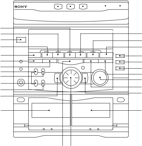
LOCATION OF PARTS AND CONTROLS
|
1 |
2 |
3 |
|
|
|
4 |
|
5 |
|
|||||||||||||||
|
|
|
|
|
|
|
|
|
|
|
|
|
|
|
|
|
|
|
|
|
|
|
|
|
|
|
|
|
|
|
|
|
|
|
|
|
|
|
|
|
|
|
|
|
|
|
|
|
|
|
|
|
|
|
|
|
|
|
|
|
|
|
|
|
|
|
|
|
|
|
|
|
|
|
|
|
|
#¡ |
#º |
@ª |
@• |
@¶ |
@§ |
@ @¢ @£ @™
@¡
@º
!ª
!• !¶
6 |
7 |
8 |
9 |
0 |
!¡ |
!™ |
!£ |
!¢ |
! |
!§ |
1 DISC 1 button
2 DISC 2 button
3 DISC 3 button
4DISC SKIP button
5 §OPEN/CLOSE button
6 ·(TAPE B)
7 · (CD) button
8 TUNER/BAND button
9 r REC button !º PAUSE button !¡ CD SYNC button
!™ STEREO/MONO button !£ VOLUME
!¢ REPEAT/MEMORY button
! ‚+ button !§ DECK B
!¶ JOG DIAL
!• (STOP) button !ª DECK A
@º º– button @¡ DBFB button
@™ SURROUND button @£ FILE SELECT button @¢ DISPLAY/DEMO button
@ EDIT/DIRECTION button @§ PLAY MODE button
@¶ FUNCTION
@• ª(TAPE A) button @ª I/u (POWER) button #º ·(TAPE A) button #¡ ª(TAPE B) button
— 4 —

SECTION 2
DISASSEMBLY
Note : Follow the disassembly procedure in the numerical order given.
2-1. UPPER COVER AND CD DOOR
4 Upper cover
6 CD door
3 Seven screws
2 Three screws
claws
1 Three srews
5 Pull out the CD tray and remove the CD door with releasing craws into the directioin of arrow.
2-2. FRONT PANEL
4 Flat type wire (CN09)
5 Front panel
1 Three screws
3Flat type wire (CN09)
2Connector (CN302)
— 5 —
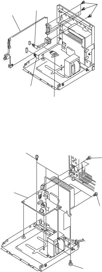
2-3. MAIN BOARD
1 Five screws
4 Harness (CN08)
5 MAIN board
3 Harness (CN302)
2 Harness (CN701)
2-4. AMP BOARD
4 Three screws
1 Two screws
5 AMP board
2 Three screws
3 Three screws
— 6 —
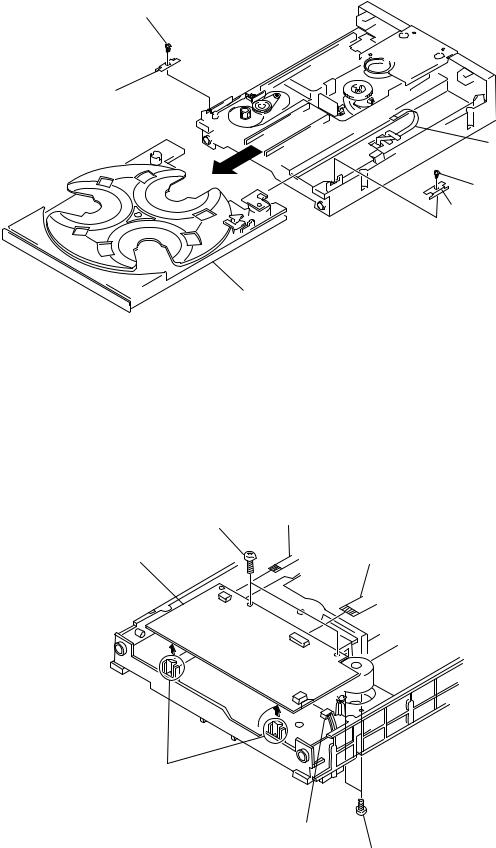
2-5. CD TRAY
1 Screw
2 Bracket
5 Flat type wire (CN06)
3 Screw
4 Bracket
6 CD tray
2-6. CD DECODER BOARD
2 Two screws |
3 Flat cable |
6 CD decoder board |
4 Flat cable |
claws
5 Connector
1 Two screws
— 7 —
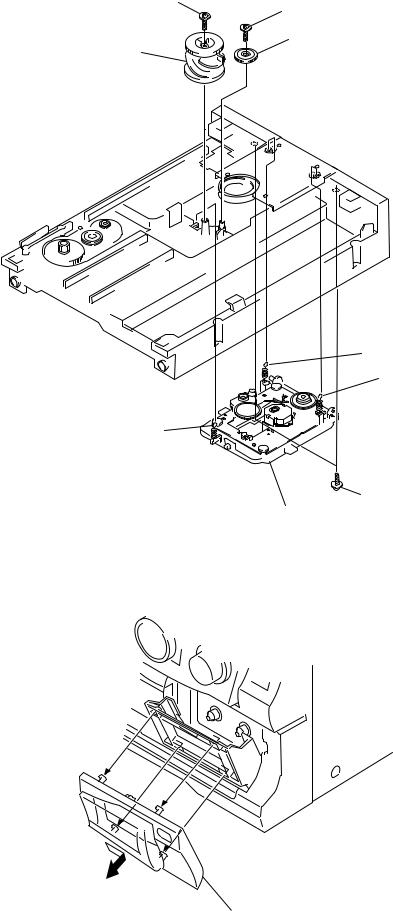
2-7. BASE UNIT
4 Screw
2 Screw
3 UD-gear
5 UD-Cam
7 Spring
6 Spring
8 Spring
1 Two screws
9 Base unit
2-8. CASSETTE DOOR
Cassette door
(Note: Four claws are used.)
— 8 —
SECTION 3
MECHANICAL ADJUSTMENTS
Precaution
1.Clean the following parts with a denatured alcohol-moistened swab:
record/playback head |
pinch rollers |
erase head |
rubber belts |
capstan |
idlers |
2.Demagnetize the record/playback head with a head demagnetizer.
3.Do not use a magnetized screwdriver for the adjustments.
4.After the adjustments, apply suitable locking compound to the parts adjusted.
5.The adjustments should be performed with the rated power supply voltage unless otherwise noted.
Torque Measurement
Torque |
Torque meter |
Meter reading |
|
|
|
|
|
FWD |
CQ-102C |
40 to 70 g • cm |
|
(0.56 - 0.97 oz • inch) |
|||
|
|
||
|
|
|
|
FWD |
CQ-102C |
1 to 5 g • cm |
|
back tension |
(0.01 - 0.07 oz • inch) |
||
|
|||
|
|
|
|
FF/REW |
CQ-201B |
55 to 140 g • cm |
|
(0.76 - 1.94 oz • inch) |
|||
|
|
SECTION 4
ELECTRICAL ADJUSTMENTS
DECK SECTION |
|
0 dB=0.775V |
|
|
|
1.Demagnetize the record/playback head with a head damagnetizer.
2.Do not use a magnetized screwdriver for the adjustments.
3.After the adjustments, apply suitable locking compound to the parts adjusted.
4.The adjustments should be performed with the rated power supply voltage unless otherwise noted.
5.The adjustments should be performed in the order given in this service manual. (As a general rule, playback circuit adjustment should be completed before performing recording circuit adjustment.)
6.The adjustments should be performed for both L-CH and R- CH.
Tape |
Signal |
Used for |
|
|
|
P-4-A100 |
10 kHz, –10 dB |
Azimuth Adjustment |
|
|
|
WS-48B |
3 kHz, 0 dB |
Tape Speed Adjustment |
|
|
|
Record/Playback Head Azimuth Adjustment
(Deck A, Deck B)
Note: Perform this adjustments for both decks.
Procedure:
1.Mode : Playback
test tape |
|
|
P-4-A100 |
|
|
(10kHz, –10dB) |
SPEAKER |
level meter |
|
||
|
|
|
|
terminal (JK301) |
|
set |
|
+ |
|
|
– |
— 9 —

2.Turn the adjustment screw and check output peaks. If the peaks do not match for L-CH and R-CH, turn the adjustment screw so that outputs match within 2 dB of peak.
4.After the adjustments, apply suitable locking compound to the parts adjusted.
Adjustment Location:
L-CH |
|
|
|
peak |
|
|
|
output |
within |
|
|
level |
|
||
2dB |
within 2dB |
||
|
R-CH
peak
screw position
L-CH |
R-CH |
|
screw |
|
|||
|
position |
||
peak |
peak |
|
|
|
|
3.Mode: Playback
test tape P-4-A100 (10kHz, –10dB)
SPEAKER terminal (JK301)
(L-CH)
oscilloscope
L
set
 R
R
SPEAKER terminal (JK301) (R-CH)
Waveform of oscilloscope
in phase |
45˚ |
90˚ |
135˚ |
180˚ |
|
good |
|
|
wrong |
Adjustment screws REC/PB head (deck A) or PB head (deck B)
Tape Speed Adjustment (Deck A)
Procedure:
1. Mode: Playback
test tape |
|
WS-48B |
frequency counter |
(3kHz, 0dB) |
|
set |
+ |
|
– |
SPEAKER terminal (JK301)
2.Adjust the SFR501 so that the frequency counter reads 3,000 Hz ± 90Hz.
Adjustment Location: DECK board
Sample Value of Wow and flutter
W. RMS (JIS) within 0.3% (test tape: WS-48B)
[DECK BOARD] — Component side —
Tape Speed
CN501
SFR501
— 10 —
TUNER SECTION |
|
0 dB=1µV |
|
|
|
MW Tuning Voltage Adjustment
Main board |
DC voltmeter |
|
|
TP1 |
F |
|
G |
|
VT |
+ |
|
– |
Procedure:
1.Set the reception frequency of the unit to 531 kHz.
2.Adjust L105 for 1.2 ± 0.05 V reading on the DC voltmeter.
3.Set the reception frequency of the unit to 1,602 kHz.
4.Confirm that the voltage reading on the DC voltmeter is within 8.0 ± 0.5 V.
Adjustment Location: MAIN board (See page 12)
AM Tracking Adjustment
|
loop antenna |
|
loop antenna |
|
|
(Supplied accessories) |
|
AM RF SSG |
|
|
|
|
|
|
set |
30% amplitude |
|
60 cm |
AM ANTENNA |
|
terminal (JK101) |
||
modulation by |
|
|
|
|
|
|
|
400 Hz signal |
Field strength dB ( V/m) =SSG output level dB ( V/m) –26 dB. |
||
Procedure:
1.Tune the set to 600 kHz.
2.Set the output of AM RF SSG so that the input level of the set will become 60 dB (µV/m).
3.Adjust L104 so that when the waveform on the oscilloscope is maximum, no noise appears.
4.Tune the set to 1,400 kHz.
5.Adjust CT102 so that when the waveform on the oscilloscope is maximum, no noise appears.
• Repeat the procedures in each adjustment several times, and the tracking adjustment should be finally done by the trimmer capacitors.
Adjustment Location: MAIN board (See page 12)
— 11 —
FM Tuned Level Adjustment
FM RF SSG
75 Ω coaxial
set
Carrier frequency |
: |
98 MHz |
Modulation |
: AUDIO 1 kHz, 75 kHz |
|
|
|
deviation (100%) |
Output level |
: |
28 dB (at 75 Ω open) |
FM ANTENNA terminal (JK101)
Procedure:
1.Supply a 28 dB 98 MHz signal from the ANTENNA terminal.
2.Tune the set to 98 MHz.
3.Adjust SFR101 to the point (moment) when the TUNED indicator will change from going off to going on.
Adjustment Location: MAIN board
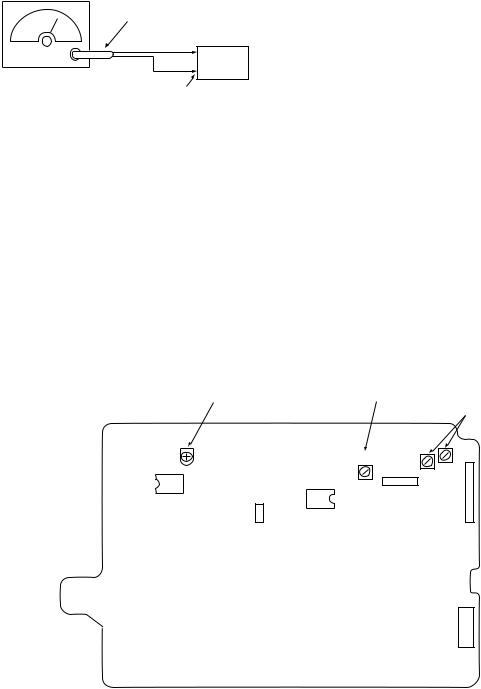
Adjustment Location
[MAIN BOARD] — Component side —
FM Tyned Level |
MW Tuning |
|
|
Voltage |
AM |
||
|
|
||
|
|
Tracking |
|
|
CT102 |
L104 |
|
SFR101 |
L105 |
||
|
|||
|
IC101 |
JK101 |
|
|
IC102 |
|
TP1
IC103
JK301
— 12 —
CD SECTION
Note:
1.CD Block is basically constructed to operate without adjustment. Therefore, check each item in order given.
2.Use YEDS-18 disc (3-702-101-01) unless otherwise indicated.
3.Use an oscilloscope with more than 10MW impedance.
4.Clean the object lens by an applicator with neutral detergent when the signal level is low than specified value with the following checks.
5.Adjust the focus bias adjustment when optical block is replaced.
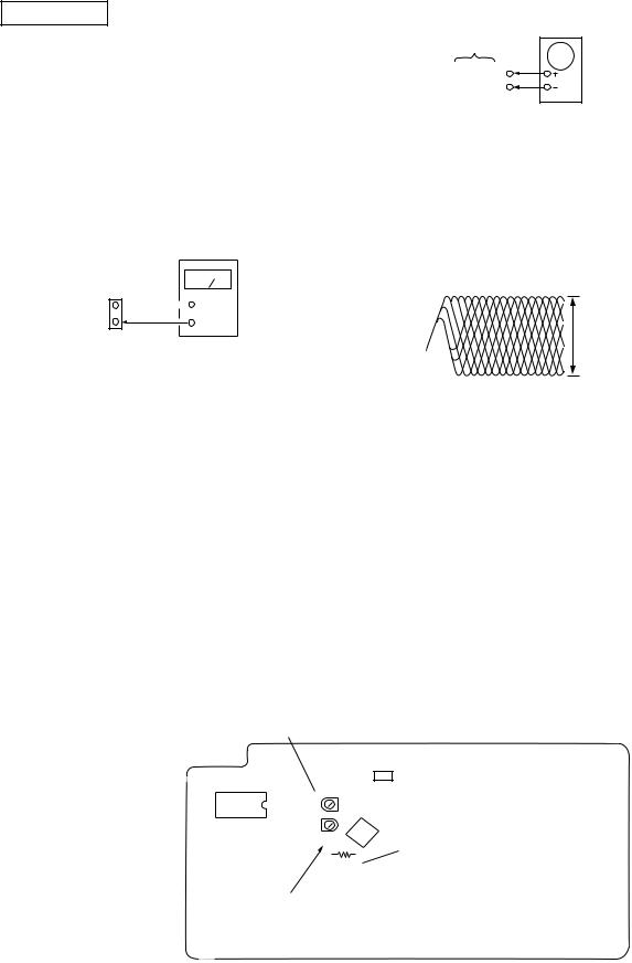
Focus Bias Adjustment
DC voltmeter
CD DECODER board
RF Level Check
CD DECODER |
oscilloscope |
|
|
board |
|
TP (RF) |
|
CN12 (VC) |
|
Procedure :
1.Connect oscilloscope to test point TP (RF) on CD DECODER board.
2.Turned Power switch on.
3.Put disc (YEDS-18) in and playback.
4.Confirm that oscilloscope waveform is clear and check RF signal level is correct or not.
Note: Clear RF signal waveform means that the shape “ à” can be clearly distinguished at the center of the waveform.
CN12
FEO  +
+
VC |
– |
Procedure:
1.Connect DC voltmeter to test point CN12 (FEO), (VC) on CD DECODER board.
2.Turned Power switch on.
3.Put disc (YEDS-18) in and stop.
4.Adjust VR01 so that the DC voltmeter reading is 0 ± 20 mV.
Adjustment Location: CD DECODER board
Focus Gain Adjustment (VR02)
This gain has a margin, so even if it is slightly off. There is no problem.
Therefore, do not perform this adjustment.
Please note that it should be fixed to mechanical center position when you moved and do not know original position.
VOLT/DIV: 200 mV
TIME/DIV: 500 nS
+0.3 level: 1.0 –0.2 Vp-p
Adjustment Location: CD DECODER board
Adjustment Location
[CD DECODER BOARD] — Component side —
Focus Gain
CN12
 VR02
VR02
IC03
IC01
VR01
RF Level
R07
Focus Bias
— 13 —
 Loading...