


HCD-RX77
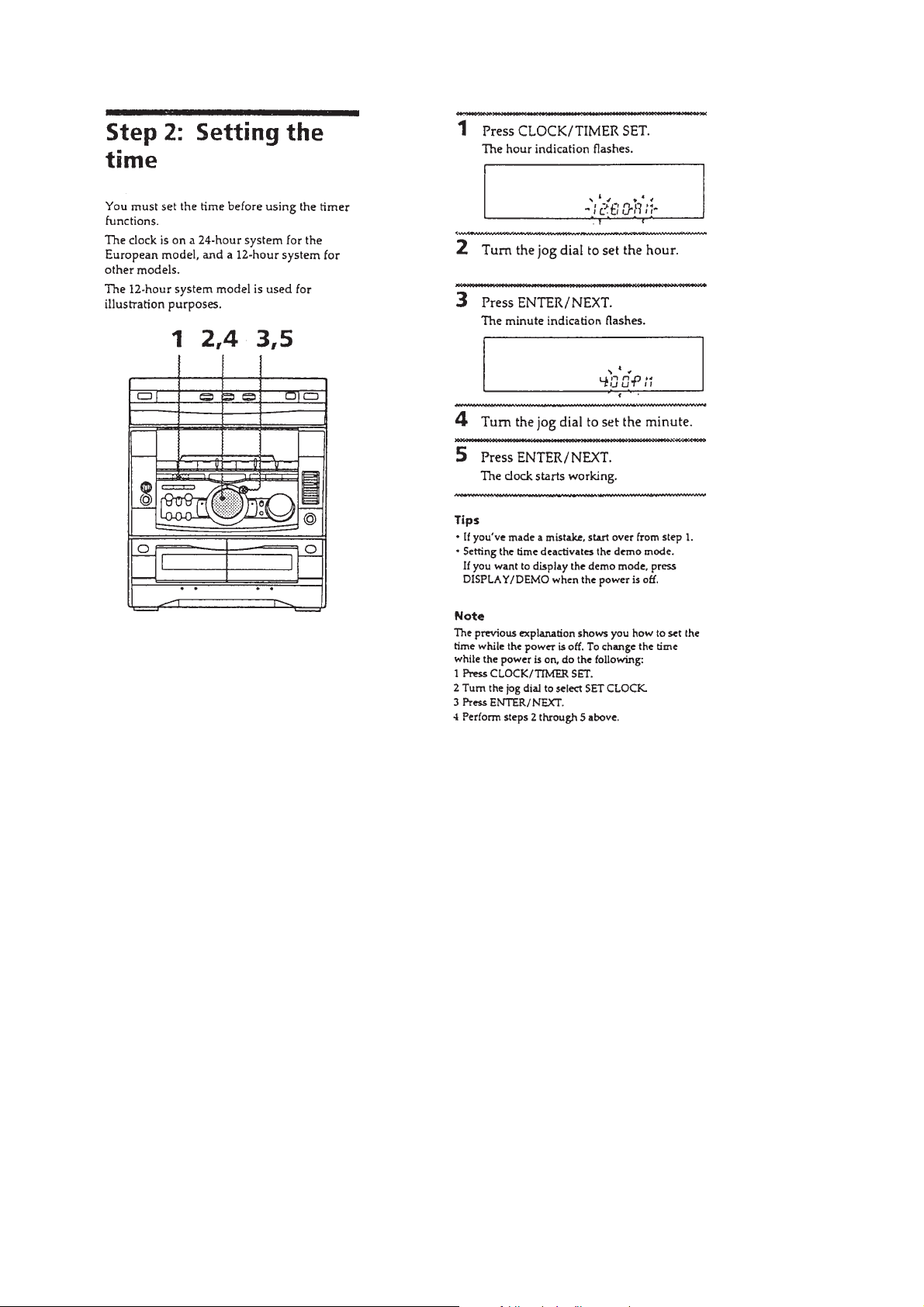
Table of contents
 Loading...
MICROFILM
SERVICE MANUAL
MINI Hi-Fi COMPONENT SYSTEM
Canadian Model
HCD-RX77
AEP Model
HCD-R700/RX77/RX77S
UK Model
HCD-R700/RX77S
E Model
HCD-GRX7/GRX7J
Austr alian Model
HCD-GRX7
Tourist Model
HCD-GRX7J
Model Name Using Similar Mechanism HCD-H991AV
CD Mechanism Type
CDM38L-5BD29AL/
CDM38LH-5BD29AL
Base Unit Type BU-5BD29AL
Optical Pick-up Type KSS-213D/Q-NP
Model Name Using Similar Mechanism NEW
Tape Transport Mechanism Type
TCM-230AWR1/
230PWR1
HCD-GRX7/GRX7J/R700/
RX77/RX77S
HCD-GRX7/GRX7J/R700/RX77/RX77S
are the Amplifier, CD player, Tape Deck
and Tuner section in MHC-GRX7/
GRX7J/R700/RX77/RX77S.
Photo: HCD-RX77
Dolby noise reduction manufactured under license
from Dolby Laboratories Licensing Corporation.
“DOLBY” and the double-D symbol a are trade-
marks of Dolby Laboratories Licensing Corporation.
CD
Section
T APE
DECK
Section
SPECIFICA TIONS
Amplifier section
Canadian model:
Continuous RMS power output (reference)
100 + 100 watts
(8 ohms at 1 kHz, 10% THD)
Total harmonic distortion less than 0.07%
(8 ohms at 1 kHz, 55 W)
European and Russian models:
DIN power output (rated) 60 + 60 watts
(6 ohms at 1 kHz, DIN)
Continuous RMS power output (reference)
80 + 80 watts
(6 ohms at 1 kHz, 10% THD)
Music power output (reference)
135 + 135 watts
(6 ohms at 1 kHz, 10% THD)
Other models:
The following measured at AC 110, 220 V 50/60 Hz
DIN power output (rated) 85 + 85watts
(8 ohms at 1 kHz, DIN)
Continuous RMS power output (reference)
110 + 110 watts
(8 ohms at 1 kHz, 10% THD)
The following measured at AC 120, 240 V 50/60 Hz
DIN power output (rated) 105 + 105 watts
(8 ohms at 1 kHz, DIN)
Continuous RMS power output (reference)
130 + 130 watts
(8 ohms at 1 kHz, 10% THD)
Peak music power output (reference)
1500 watts
– Continued on next page –

– 2 –
Specifications (continued)
Inputs
MD/VIDEO IN: voltage 450 mV/250mV,
(phono jacks) impedance 47 kilohms
MIX MIC: (phone jack) sensitivity 1 mV, impedance 10
kilohms
Outputs
MD/VIDEO OUT: voltage 250 mV,
(phono jacks) impedance 1 kilohms
PHONES: accepts headphones of 8 ohms
(stereo phone jack) or more
SPEAKER:
European and Russian models: accepts impedance of 6 to 16 ohms
Other models: accepts impedance of 8 to 16 ohms
SURROUND SPEAKER (Canadian model):
accepts impedance of 16 ohms
SUPER WOOFER (GRX7/GRX7J/RX77: Canadian models):
Voltage 1 V, impedance 1 kilohm
CD player section
System Compact disc and digital audio system
Laser Semiconductor laser (λ=780nm)
Emission duration: continuous
Laser output Max. 44.6 µW*
*This output is the value measured at
distance of 200 mm from the objective
lens surface on the Optical Pick-up
Block with 7 mm aperture.
Frequency response 2 Hz - 20 kHz (±0.5 dB)
Wavelength 780 -790 nm
Signal-to-noise ratio More than 90 dB
Dynamic range More than 90 dB
CD OPTICAL DIGITAL OUT
(Square optical connector jack, rear panel)
Wavelength 600 nm
Output Level -18 dBm
Tape player section
Recording system 4-track 2-channel stereo
Frequency response 40 - 13,000 Hz (±3 dB),
(DOLBY NR OFF) using Sony TYPE I cassette
40 - 14,000 Hz (±3 dB),
using Sony TYPE II cassette
Tuner section
FM stereo, FM/AM superheterodyne tuner
FM tuner section
Tuning range 87.5 - 108.0 MHz
Antenna FM lead antenna
Antenna terminals 75 ohm unbalanced
Intermediate frequency 10.7 MHz
UKV tuner section (4 band models only)
Tuning range 65.0 - 74.0 MHz
Stereo Plus
AM tuner section
Tuning range
2 Band type:
Canadian model: 530 - 1,710 kHz
(with the interval set at 10 kHz)
531 - 1,710 kHz
(with the interval set at 9 kHz)
Other model: 531 - 1,602 kHz
(with the interval set at 9 kHz)
530 - 1,710 kHz
(with the interval set at 10 kHz)
3 Band/4 Band type:
European and Russian models:
MW: 531 - 1,602 kHz
(with the interval set at 9 kHz)
LW: 153 - 279 kHz
(with the interval set at 3 kHz)
Middle Eastern models:
MW: 531 - 1,602 kHz
(with the interval set at 9 kHz)
SW: 5.95 - 17.90 MHz
(with the interval set at 5 kHz)
Other models:
MW: 531 - 1,602 kHz
(with the interval set at 9 kHz)
530 - 1,710 kHz
(with the interval set at 10 kHz)
SW: 5.95 - 17.90 MHz
(with the interval set at 5 kHz)
Antenna AM loop antenna
Antenna terminals External antenna terminal
Intermediate frequency 450 kHz
General
Power requirements
Canadian model: 120 V AC, 60 Hz
European and Russian models: 230 V AC, 50/60 Hz
Mexican model: 120 V AC, 50/60 Hz
Australian and Israel models: 220 - 240 V AC, 50/60 Hz
Thai model: 220 - 240 V AC, 50/60 Hz
Other models: 110 - 120 V or 220 - 240 V AC,
50/60 Hz
Power consumption
Canadian model: 195 watts
European and Russian models: 140 watts
Other models: 250 watts
Dimensions (w/h/d) Approx. 280 × 335 × 380 mm
(11
1
/8 × 13
1
/8 × 15 in.)
Mass
Canadian model: Approx. 9.5 kg (20 lbs. 15 oz.)
European and Russian models: Approx. 9.1 kg (20 lbs. 1 oz.)
Other models: Approx. 10.2 kg (22 lbs. 8 oz.)
Supplied accessories: AM loop antenna (1)
Remote RM-SR5 (1)
Batteries (2)
FM lead antenna (1)
Speaker cords (2)
Front speaker pads (8)
Design and specifications are subject to change without notice.
– 3 –
1. SERVICING NOTES............................................... 3
2. GENERAL
Location of Controls ....................................................... 6
Setting the Time .............................................................. 7
3. DISASSEMBLY ......................................................... 8
4. TEST MODE.............................................................. 11
5. MECHANICAL ADJUSTMENTS....................... 13
6. ELECTRICAL ADJUSTMENTS
DECK Section ................................................................. 13
TUNER Section .............................................................. 16
CD Section ...................................................................... 18
7. DIAGRAMS.................................................................20
7-1. Block Diagram – TUNER Section
(AEP, UK, German models only) – ................................ 21
7-2. Block Diagram – TUNER Section
(East European, CIS models only) – .............................. 23
7-3. Block Diagram
– CD MECHANISM DECK Section – .......................... 25
7-4. Block Diagram – TAPE DECK Section – ...................... 27
7-5. Block Diagram – MAIN Section – ................................. 29
7-6. Block Diagram – DISPLAY/KEY CONTROL/
POWER SUPPLY Section – ......................................... 31
7-7. Schematic Diagram – TUNER Section
(AEP, UK, German models only) – ................................ 35
7-8. Printed Wiring Board – TUNER Section
(AEP, UK, German models only) – ................................ 37
7-9. Printed Wiring Board – TUNER Section
(East European, CIS models only) – .............................. 38
7-10. Schematic Diagram – TUNER Section
(East European, CIS models only) – .............................. 39
7-11. Printed Wiring Board – CD Section – ........................... 41
7-12. Schematic Diagram – CD Section – ............................... 43
7-13. Printed Wiring Boards – CD MOTOR Section – .......... 45
7-14. Schematic Diagram – CD MOTOR Section – .............. 47
7-15. Printed Wiring Board – TAPE DECK Section – ........... 49
7-16. Schematic Diagram – TAPE DECK Section –.............. 51
7-17. Printed Wiring Board – LEAF SW Section – ............... 53
7-18. Schematic Diagram – LEAF SW Section – .................. 53
7-19. Printed Wiring Board – MAIN Section –...................... 55
7-20. Schematic Diagram – MAIN Section (1/4) –............... 57
7-21. Schematic Diagram – MAIN Section (2/4) –................ 59
7-22. Schematic Diagram – MAIN Section (3/4) –................ 61
7-23. Schematic Diagram – MAIN Section (4/4) –................ 63
7-24. Printed Wiring Board – PANEL Section – .................... 65
7-25. Schematic Diagram – PANEL Section –....................... 67
7-26. Printed Wiring Board – CD-SW Section –.................... 69
7-27. Schematic Diagram – CD-SW Section – ...................... 69
7-28. Printed Wiring Board – HP Section – ........................... 71
7-29. Schematic Diagram – HP Section – .............................. 71
7-30. Printed Wiring Board – POWER AMP Section – ......... 72
7-31. Schematic Diagram – POWER AMP Section –............ 73
7-32. Printed Wiring Board
– TRANSFORMER Section – ........................................ 75
7-33. Schematic Diagram
– TRANSFORMER Section – ........................................ 76
7-34. IC Pin Function Description ........................................... 82
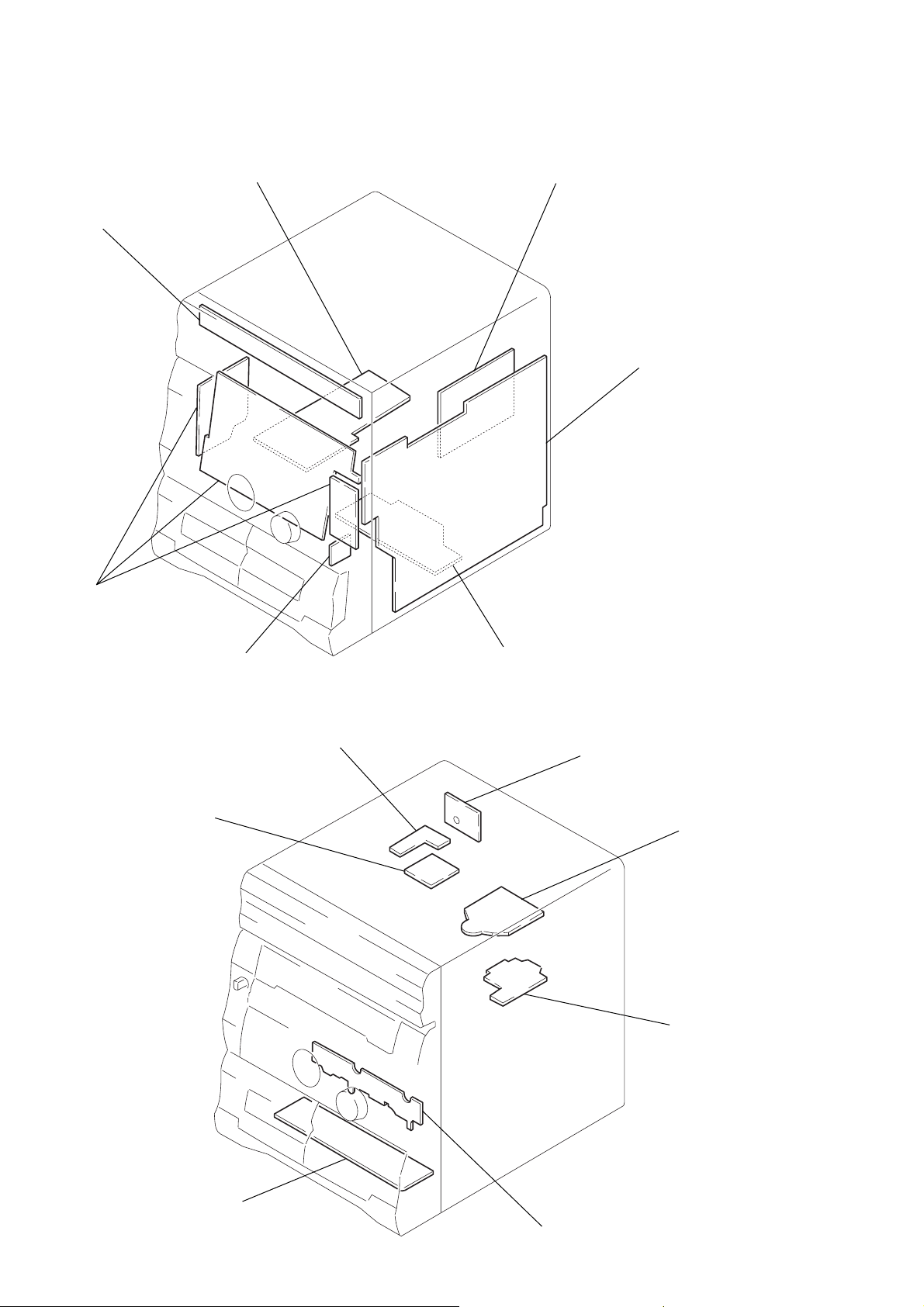
8. EXPLODED VIEWS ................................................ 87
9. ELECTRICAL PARTS LIST ............................... 96
TABLE OF CONTENTS
The laser diode in the optical pick-up block may suffer electro-
static break-down because of the potential difference generated
by the charged electrostatic load, etc. on clothing and the human
body.
During repair, pay attention to electrostatic break-down and also
use the procedure in the printed matter which is included in the
repair parts.
The flexible board is easily damaged and should be handled with
care.
NOTES ON LASER DIODE EMISSION CHECK
The laser beam on this model is concentrated so as to be focused
on the disc reflective surface by the objective lens in the optical
pick-up block. Therefore, when checking the laser diode emis-
sion, observe from more than 30 cm away from the objective lens.
Notes on chip component replacement
• Never reuse a disconnected chip component.
• Notice that the minus side of a tantalum capacitor may be dam-
aged by heat.
Flexible Circuit Board Repairing
• Keep the temperature of the soldering iron around 270 ˚C dur-
ing repairing.
• Do not touch the soldering iron on the same conductor of the
circuit board (within 3 times).
• Be careful not to apply force on the conductor when soldering
or unsoldering.
NOTES ON HANDLING THE OPTICAL PICK-UP
BLOCK OR BASE UNIT
CAUTION
Use of controls or adjustments or performance of procedures
other than those specified herein may result in hazardous ra-
diation exposure.
This appliance is classified as a CLASS 1 LASER product.
The CLASS 1 LASER PRODUCT MARKING is located on
the rear exterior.
Laser component in this product is capable of emitting radiation
exceeding the limit for Class 1.
The following caution label is located inside the unit.
CAUTION : INVISIBLE LASER RADIATION WHEN OPEN AND
INTERLOCKS DEFEATED. AVOID EXPOSURE TO BEAM.
ADVARSEL : USYNLIG LASERSTRÅLING VED ÅBNING NÅR
SIKKERHEDSAFBRYDERE ER UDE AF FUNKTION. UNDGÅ UDSAETTELSE
FOR STRÅLING.
VORSICHT : UNSICHTBARE LASERSTRAHLUNG, WENN
ABDECKUNG GEÖFFNET UND SICHEREITSVERRIEGELUNG
ÜBERBRÜCKT. NICHT DEM STRAHL AUSSETZEN.
VARO
!
: AVATTAESSA JA SUOJALUKITUS OHITETTAESSA OLET ALT-
TIINA NÄKYMÄTTÖMÄLLE LASERSÄTEILYLLE. ÄLÄ KATSO SÄTEESEEN.
VARNING : OSYNLING LASERSTRÅLING NÄR DENNA DEL ÄR ÖPPNAD
OCH SPÄRREN ÄR URKOPPLAD. BETRAKTA EJ STRÅLEN.
ADVERSEL : USYNLIG LASERSTRÅLING NÅR DEKSEL ÅPNES OG
SIKKERHEDSLÅS BRYTES. UNNGÅ EKSPONERING FOR STRÅLEN.
VIGYAZAT
!
: A BURKOLAT NYITÁSAKOR LÁTHATATLAN LÉZERSU-
GÁRVESZÉLY
!
KERÜLJE A BESUGÁRZÁST
!
SECTION 1
SERVICING NOTES
– 4 –
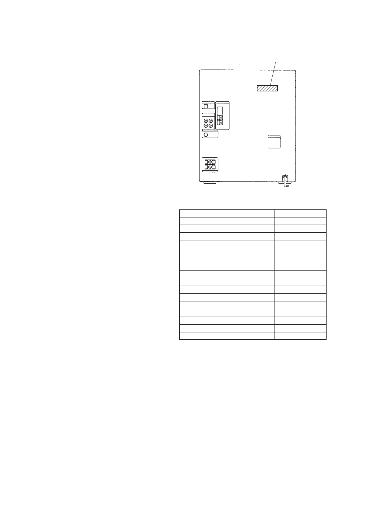
PART No.
MODEL IDENTIFICATION
– Back Panel –
MODEL PART No.
Canadian model 4-996-843-0π
Israel and Thai models 4-996-843-6π
E model 4-996-844-0π
Malaysia, Singapore and
4-996-844-1π
South African models
GRX7: Saudi Arabia and Taiwan models 4-996-844-2π
Hong Kong model 4-996-844-3π
Australian model 4-996-844-4π
Mexican model 4-996-844-5π
Indonesian model 4-996-844-7π
GRX7J 4-996-844-8π
RX77S: UK model 4-996-845-0π
RX77S: East European and CIS model 4-996-845-1π
R700 4-996-845-2π
RX77: AEP and German model 4-996-845-3π
RX77: East European model 4-996-845-4π
ATTENTION AU COMPOSANT AYANT RAPPORT
À LA SÉCURITÉ!
LES COMPOSANTS IDENTIFIÉS P AR UNE MARQ UE !
SUR LES DIAGRAMMES SCHÉMATIQUES ET LA LISTE
DES PIÈCES SONT CRITIQUES POUR LA SÉCURITÉ
DE FONCTIONNEMENT. NE REMPLACER CES COM-
POSANTS QUE PAR DES PIÈCES SONY DONT LES
NUMÉROS SONT DONNÉS DANS CE MANUEL OU
DANS LES SUPPLÉMENTS PUBLIÉS PAR SONY.
SAFETY-RELATED COMPONENT WARNING!!
COMPONENTS IDENTIFIED BY MARK ! OR DOTTED
LINE WITH MARK ! ON THE SCHEMATIC DIAGRAMS
AND IN THE PARTS LIST ARE CRITICAL TO SAFE
OPERATION. REPLACE THESE COMPONENTS WITH
SONY PARTS WHOSE PART NUMBERS APPEAR AS
SHOWN IN THIS MANUAL OR IN SUPPLEMENTS PUB-
LISHED BY SONY.
– 5 –
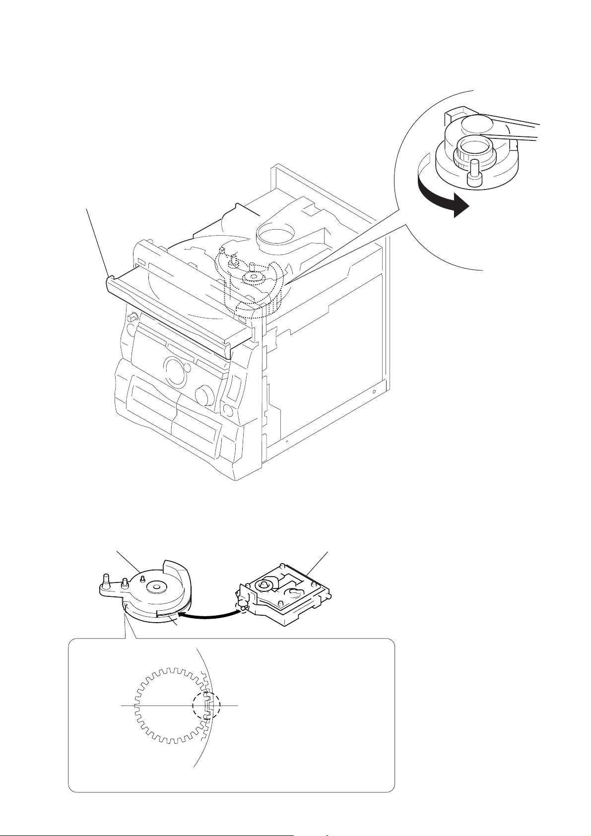
HOW TO OPEN THE DISC TRAY WHEN POWER SWITCH TURNS OFF.
1
Remove the Case.
3
Pull-out the disc tray.
2
Turn the cam to the
direction of arrow.
NOTE FOR INSTALLATION (ROTARY ENCODER)
BU cam
Groove
Section A
Note:When attaching the Base unit, Insert th
e
section A into the groove of BU cam.
Note:When attaching the BU cam,
engage the Rotary encoder
switch as shown in the figure.
– 6 –
SECTION 2
GENERAL
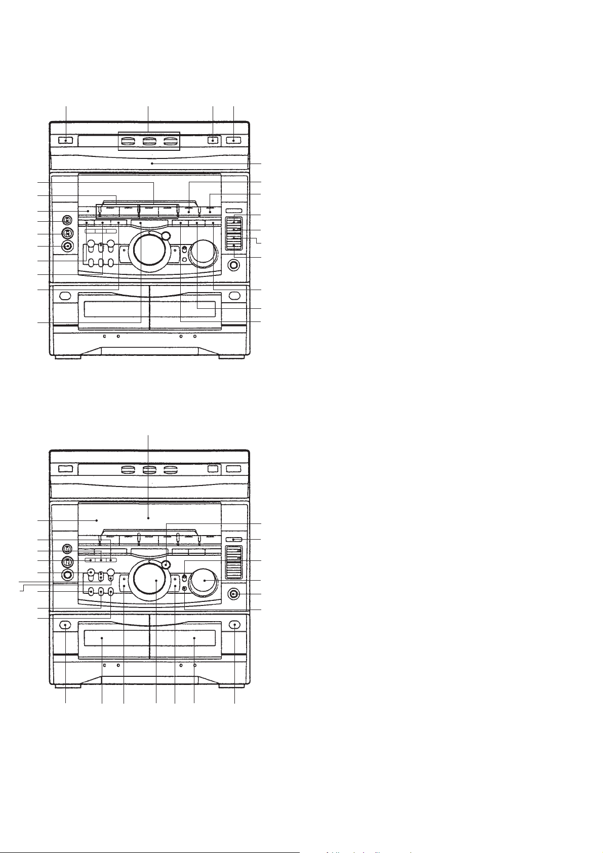
LOCATION OF CONTROLS
1 2 3 4
!¶
!§
!∞
!ª
@º
@¡
@™
@£
@¢
5
6
7
8
9
!º
!¡
!™
!£
!¢
@∞
#™
#£
#∞
#§
#ª
$º
$¡
@¶
@•
@ª
#º
#¡
$™ $£ $¢ $∞ $§ $¶ $•
1 I /u (Power) button
2 DISC 1 to 3 buttons and indicators
3 DISC SKIP/EX-CHANGE button
4 6 (CD) button
5 CD disc tray
6 CD ^ button and indicator
7 TUNER, BAND button
8 r REC button and indicator
9 P PAUSE button and indicator
!º HI-DUB button
!¡ CD SYNC button
!™ EFFECT button and indicator
(GRX7/GRX7J/RX77: Canadian models)
FILE SELECT button (AEP, UK, German, East
European, and CIS models)
!£ SURROUND button
!¢ KARAOKE PON/MPX button
!∞ DECK B 9 and ( buttons and indicators
!§ DECK A 9 and ( buttons and indicators
!¶ FUNCTION button
!• ECHO LEVEL knob (Saudi Arabia model)
!ª MIC LEVEL knob
@º MIX MIC jac
@¡ DISPLAY/DEMO button
@™ CLOCK/TIMER SET button
@£ TIMER SELECT button
@¢ p button
@∞ Fluorescent indicator tube
@§ ENTER/NEXT button and indicator
@¶ PTY button (AEP, UK, and German models)
@• GROOVE button and indicator
@ª VOLUME konb
#º PHONES jack
#¡ DBFB button
#™ Remote sensor
#£ P FILE MEMOR Y button (GRX7/GRX7J/RX77:
Canadian models)
#¢ GEQ CONTROL button (GRX7/GRX7J/RX77:
Canadian models)
#∞ FILE SELECT button (GRX7/GRX7J/RX77:
Canadian models)
#§ LOOP button
#¶ NON-STOP button and indicator
#• FLASH button
#ª EDIT, DIRECTION button
$º PLAY MODE, DOLBY NR button
$¡ REPEAT button
$™ § button (deck A)
$£ Tape deck A
$¢ –, 0 button and indicator
$∞ JOG dial
$§ +, ) button and indicator
$¶ Tape deck B
$• § button (deck B)
!•
@§
#¢
#•
#¶
– 7 –
– 8 –
CASE
FRONT PANEL SECTION
Note: Follow the disassembly procedure in the numerical order given.
SECTION 3
DISASSEMBLY
1
three screws
(BVTP3
×
8)
2
screw
(CASE3 TP2) (3
×
12)
3
two screws
(CASE3 TP2) (3
×
8)
6
case
2
screw
(CASE3 TP2) (3
×
12)
3
two screws
(CASE3 TP2) (3
×
8
)
4
4
5
3
two claws
4
loading panel
1
Turn the cam to the direction
of arrow
A
.
A
9
screw
(BVTP3
×
10)
2
Pull-out the
disc tray.
0
three screws
(BVTT3
×
6)
8
connector
(CN109)
9
screw
(BVTP3
×
10)
6
wire (flat type) (13 core)
(23 cm) (CN201)
7
wire (flat type)
(17 core) (CN107)
5
wire (flat type)
(15 core) (33 cm)
(CN106)
– 9 –
TAPE MECHANISM DECK SECTION (TCM-230AWR1/TCM-230PWR1)
CD MECHANISM DECK SECTION (CDM38L-5BD29AL /CDM38LH-5BD29AL)
1
Push the
cassette lids.
3
three screws
(BVTP3
×
8)
2
Open the
cassette lids.
4
two screws
(BVTP3
×
8 )
5
tape mechanism
deck section
(TCM-230AWR1/
TCM-230PWR1)
4
CD mechanism deck section
CDM38L-5BD29AL
CDM38LH-5BD29AL
3
two screws
(BVTP3
×
8)
2
wire (flat type) (19 core) (24 cm)
(CN105)
1
two connectors
(CN103, CN104)
Note: The CD mechanism deck will
fall if three screws are removed.
Support it by hand, then remove
three screws.
– 10 –
MAIN BOARD
Abbreviation
AUS : Australian
CND : Canadian
E2 : 120 V AC Area in E model
E3 : 240 V AC Area in E model
EA3 : Saudi Arabia
EA4 : Israel
EE : East European
G : German
HK : Hong Kong
IA : Indonesian
MX : Mexican
MY : Malaysia
SAF : South African
SP : Singapore
TH : Thai
TW : Taiwan
3
two screws
(BVTP3
×
8)
3
screw
(BVTP3
×
8)
2
wire (flat type) (13 core) (14 cm)
(CN102) (CND, E2, EA4, TH,
MX, AUS)
wire (flat type) (15 core) (14 cm)
(CN102) (GRX7: E3, EA3, MY,
SP, IA, HK, TW, SAF/GRX7J/
R700/RX77: AEP, G, EE/RX77S
)
6
MAIN board
5
connector
(CN101)
7
connector
(CN110)
4
two screws
(BVTT3
×
6)
1
connector
(CN11)
GRX7/GRX7J
GRX7/GRX7J/RX77: CND
3
screw
(BVTP3
×
8)
3
screw
(BVTP3
×
8)
CND

– 11 –
SECTION 4
TEST MODE
[MC Cold Reset]
• The cold reset clears all data including preset data stored in the
RAM to initial conditions. Execute this mode when returning
the set to the customer.
Procedure:
1. Press three buttons p , [ENTER/NEXT], and I/u simulta-
neously.
2. The fluorescent indicator tube becomes blank instantaneously,
and the set is reset.
[CD Delivery Mode]
• This mode moves the pickup to the position durable to vibra-
tion. Use this mode when returning the set to the customer after
repair.
Procedure:
1. Press I/u button to turn the set ON.
2. Press [LOOP] button and I/u button simultaneously.
3. A message “LOCK” is displayed on the fluorescent indicator
tube, and the CD delivery mode is set.
[MC Hot Reset]
• This mode resets the set with the preset data kept stored in the
memory. The hot r eset mode functions same as if the power
cord is plugged in and out.
Procedure:
1. Press three buttons p , [ENTER/NEXT], and [DISC1] simul-
taneously.
2. The fluorescent indicator tube becomes blank instantaneously,
and the set is reset.
[Sled Servo Mode]
• This mode can run the CD sled motor freely. Use this mode, for
instance, when cleaning the pickup.
Procedure:
1. Press
I/u button to turn the set ON.
2. Select the function “CD”.
3. Press three buttons p , [ENTER/NEXT], and § simulta-
neously.
4. The Sled Servo mode is selected, if “CD” is blanking on the
fluorescent indicator tube.
5. With the CD in stop status, press ) + button to move the
pickup to outside track, or – 0 button to inside track.
6. To exit from this mode, perform as follows:
1) Move the pickup to the most inside track.
2) Press three buttons in the same manner as step 2.
Note: • Always move the pickup to most inside track when exiting from
this mode. Otherwise, a disc will not be unloaded.
• Do not run the sled motor excessively , otherwise the gear can be
chipped.
[Change-over of AM Tuner Step between 9 kHz and
10 kHz]
• A step of AM channels can be changed ov er between 9 kHz and
10 kHz.
Procedure:
1. Press I/u button to turn the set ON.
2. Select the function “TUNER”, and press [TUNER/BAND]
button to select the BAND “AM”.
3. Press I/u button to turn the set OFF.
4. Press [ENTER/NEXT] and I/u buttons simultaneously, and
the display of fluorescent indicator tube changes to “AM 9 k
STEP” or “AM 10 k STEP”, and thus the channel step is
changed over.
[LED and Fluorescent Indicator Tube All Lit, Key Check
Mode]
Procedure:
1. Press three buttons p , [ENTER/NEXT], and [DISC2] simul-
taneously.
2. LEDs and fluorescent indicator tube are all turned on.
Press [DISC2] button, and the key check mode is activated.
3. In the key check mode, the fluorescent indicator tube displays
“K 1 J0 V0”. Each time a button is pressed, “K” value in-
creases. However , once a button is pressed , it is no longer taken
into account.
“J” value increases like 1, 2, 3 ... if rotating [JOG] knob in
“+” direction, or it decreases like 0, 9, 8 ... if rotating in “–”
direction.
“V” value increases like 1, 2, 3 ... if rotating [VOLUME] knob
in “+” direction, or it decreases like 0, 9, 8 ... if rotating in
“–” direction.
4. To exit from this mode, press three buttons in the same man-
ner as step 1, or disconnect the power cord.
– 12 –
[Aging Mode]
This mode can be used for operation check of CD section and tape
deck section.
• If an error occurred:
The aging operation stops and display status.
• If no error occurs:
The aging operation continues repeatedly.
1. Operating Method of Aging Mode
1) Set disc in DISC1 tray.
2) Load the tapes recording use into the decks A and B respec-
tively.
3) Press three buttons p , [ENTER/NEXT],
and [DISCSKIP/EX-CHANGE] simultaneously.
4) The aging mode is activated, if a CD roulette mark on the fluo-
rescent indicator tube is blinking.
5) To exit from the aging mode, press I/u button to turn the set
OFF.
2. Operation Sequence
• Dur ing the aging mode in the following sequence to below.
• Starting the CD section aging for function set “CD”, starting
the TAPE section (deck A) aging for function set “TAPE A” or
“TAPE B”. (Set another function is no work.)
CD (disc1) (12 minutes) → Deck A
↑↓(About 13 minutes
Deck B 20 seconds
maximum)
3. Aging mode in CD section
1) Display state
• No error occurs
display
Note:
[*][*]
: a letter “CD” and the remainder time (minute) alternately. (re-
mainder time start from 12 minute)
@@: track number in access.
• Error occurred
2) Operation during aging Mode
In the aging mode, the program is executed in the following se-
quence.
(1) The disc tray turns to select a disc1.
(2) A disc is chucked.
(3) TOC of disc is read.
(4) The pickup accesses to the track 1, and playing 2 seconds.
(5) The pickup accesses to the last track, and playing 2 seconds.
(6) Steps 1 through 5 are repeated about 12 minutes.
(7) Change to deck section aging.
NO. Display Main factor
1 NO DISC ERR Not set disc in DISC1
2 FOCUS1 ERR Focus does not work
3 FOCUS2 ERR Focus does not work after the disc rotate as usual
4 GFS ERR GFS error
5 FBIAS ERR Error in to the focus bias adjustment
6 SENSOR ERR Disc sensor sens DISC1 is no disc
7 TABLE ERR CD tray lotate does not work
8 TRAY ERR Tray (include BD) move does not work
4. Aging mode in Ta pe Deck section
1) Display state
• No error occurs
Display action now
• Error occurred
Display action last time
2) Operation during Aging Mode
In the aging mode, the program is executed in the following se-
quence.
(1) Rewind is executed up to the top of tape.
(2) A tape on FWD side is played for 3 minutes.
(3) FF is executed up to either made for 20 minutes or the end of
tape.
(4) A tape is reversed, and the tape on REV side is played for 3
minutes.
(5) Rewind is executed up to the top of tape.
(6) Steps 1 through 5 are executed for the other deck.
(7) Change to CD section aging.
NO. Display action Action contents Final timing
1 TAPE A AG-1 Rewind the TAPE A The top of tape
2 TAPE A AG-2 FWD play the TAPE A 3 minutes playing
3 TAPE A AG-3 F.F. the TAPE A First either 20 minutes
or the end of tape
4 TAPE A AG-4 REV play the TAPE A 3 minutes playing
5 TAPE A AG-5 Rewind the TAPE A The top of tape
6 TAPE B AG-1 Rewind the TAPE B The top of tape
7 TAPE B AG-2 FWD play the TAPE B 3 minutes playing
8 TAPE B AG-3 F.F. the TAPE B First either 20 minutes
or the end of tape
9 TAPE B AG-4 REV play the TAPE B 3 minutes playing
10 TAPE B AG-5 Rewind the TAPE B The top of tape
[*][*]
1 –
@ @
– 13 –
SECTION 5
MECHANICAL ADJUSTMENTS
0 dB=0.775 V
DECK SECTION
SECTION 6
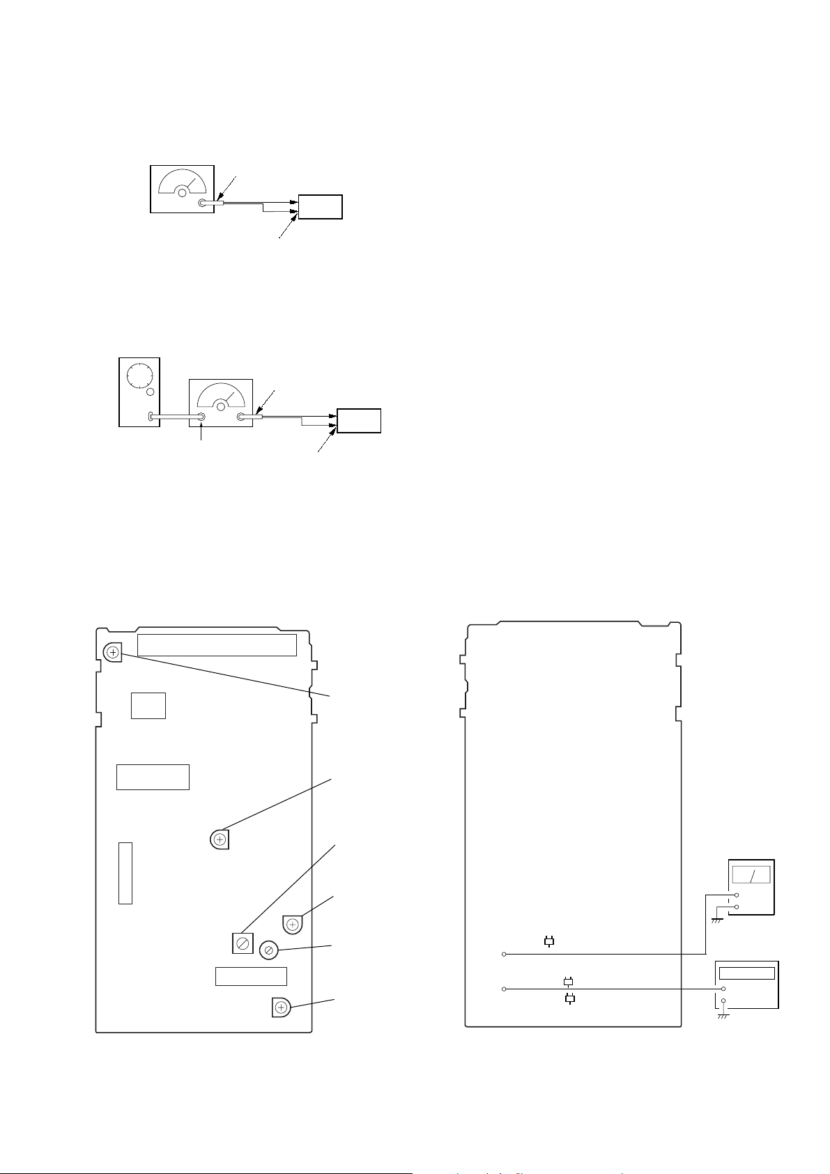
ELECTRICAL ADJUSTMENTS
Tape Signal Used for
P-4-A100 10 kHz, –10 dB Azimuth Adjustment
WS-48B 3 kHz, 0 dB Tape Speed Adjustment
P-4-L300 315 Hz, 0 dB Level Adjustment
DECK A DECK B
set
main board
CN301
Pin
3
(L-CH)
Pin
1
(R-CH)
main board
CN301
Pin
2
(GND)
+
–
level meter
test tape
P-4-A100
(10 kHz, –10 dB)
Precaution
1. Clean the following parts with a denatured alcohol-moistened
swab:
record/playback heads pinch rollers
erase head rubber belts
capstan idlers
2. Demagnetize the record/playback head with a head demagne-
tizer.
3. Do not use a magnetized screwdriver for the adjustments.
4. After the adjustments, apply suitable locking compound to the
parts adjusted.
5. The adjustments should be performed with the rated power sup-
ply voltage unless otherwise noted.
Torque Measurement
31 to 71 g • cm
(0.43 – 0.98 oz • inch)
2 to 6 g • cm
(0.03 – 0.08 oz • inch)
31 to 71 g • cm
(0.43 – 0.98 oz • inch)
2 to 6 g • cm
(0.03 – 0.08 oz • inch)
71 to 143 g • cm
(0.99 – 1.99 oz • inch)
100 g or more
(3.53 oz or more)
100 g or more
(3.53 oz or more)
Mode
FWD
Torque meter
CQ-102C
Meter reading
FWD
back tension
REV
REV
back tension
FF/REW
FWD tension
REV tension
CQ-102C
CQ-102RC
CQ-102RC
CQ-201B
CQ-403A
CQ-403R
1. Demagnetize the record/playback head with a head demagne-
tizer.
2. Do not use a magnetized screwdriver for the adjustments.
3. After the adjustments, apply suitable locking compound to the
parts adjust.
4. The adjustments should be performed with the rated power
supply voltage unless otherwise noted.
5. The adjustments should be performed in the order given in
this service manual. (As a general rule, playback circuit ad-
justment should be completed before performing recording
circuit adjustment.)
6. The adjustments should be performed for both L-CH and R-
CH.
7. Switches and controls should be set as follows unless other-
wise specified.
• Test Tape
Record/Playback Head Azimuth Adjustment
Note: Perform this adjustments for both decks
Procedure:
1. Mode: Playback
– 14 –
Screw
position
L-CH
peak
within
1dB
Output
level
L-CH
peak
R-CH
peak
within
1dB
Screw
position
R-CH
peak
MAIN
board
CN301
set
test tape
P-4-A100
(10 kHz, –10 dB)
pin
1
oscilloscope
L-CH
R-CH
V
H
waveform of oscilloscope
in phase 45
°
90
°
135
°
180
°
good
wrong
pin
2
pin
3
L
R
forward
reverse
+
–
set
test tape
WS-48B
(3 kHz, 0 dB)
main board
CN301 (Pin
3
: L-CH)
(Pin
1
: R-CH)
frequency counter
+
–
set
test tape
P-4-L300
(315 Hz, 0 dB)
main board
CN301 (Pin
3
: L-CH)
(Pin
1
: R-CH)
level meter
2. Turn the adjustment screw and check output peaks. If the peaks
do not match for L-CH and R-CH, turn the adjustment screw
so that outputs match within 1dB of peak.
3. Mode: Playback
4. After the adjustments, apply suitable locking compound to the
pats adjusted.
Adjustment Location:Playback Head (Deck A).
Record/Playback/Erase Head (Deck B).
Tape Speed Adjustment DECK B
Note: Start the Tape Speed adjustment as below after setting to the test
mode.
In the test mode, the tape speed is high during pressing the
[HI-DUB] button.
Procedure:
1. Turn the power switch on.
2. Press the p button, [ENTER/NEXT] button and [DISC3] button
simultaneously.
(The “VOLUME” on the fluorescent indicator tube will blink
while in the test mode.)
To exit from the test mode, press the I/u button.
Mode: Playback
1. Insert the WS-48B into the deck B.
2. Press the · button on the deck B.
3. Press the [HI-DUB] button in playback mode.
Then at HIGH speed mode.
4. Adjust RV1001 on the LEAF SW board do that frequency
counter reads 6,000 ± 180 Hz.
5. Press the [HI-DUB] button.
Then back to NORMAL speed mode.
6. Adjust RV1002 on the LEAF SW board so that frequency
counter reads 3,000 ± 90 Hz.
Adjustment Location: LEAF SW board
Sample value of Wow and Flutter: 0.3% or less W.RMS (JIS)
(WS-48B)
Playback level Adjustment DECK A DECK B
Procedure:
Mode: Playback
Deck A is RV311 (L-CH) and RV411 (R-CH), Deck B is RV301
(L-CH) and RV401 (R-CH) so that adjustment within adjustment
level as follows.
Adjustment Level:
CN301 PB level: 301.5 to 338.3 mV (–8.2 to –7.2 dB) level
difference between the channels: within ±0.5 dB
Adjustment Location: AUDIO board
– 15 –
REC Bias Adjustment DECK B
Procedure:
4. Mode: Record
5. Mode: Playback
6. Confirm playback the signal recorded in step 3 become ad-
justable level as follows.
If these levels do not adjustable level, adjustment the RV341
(L-CH) and RV441 (R-CH) on the AUDIO board to repeat
steps 4 and 5.
Adjustable level: Playback output of 315 Hz to playback output
of 10 kHz: ±1.0 dB
Adjustment Location: AUDIO board
REC Level Adjustment
DECK B
Procedure:
attenuator
set
MD/VIDEO (AUDIO) IN
1) 315 Hz
2) 10 kHz
50 mV (–23.8 dB)
600
Ω
blank tape
CN-123
AF OSC
+
–
set
recorded
portion
CN301 (Pin
3
: L-CH)
(Pin
1
: R-CH)
level meter
4. Mode: Record
5. Mode: Playback
6. Confirm playback the signal recorded in step 3 become ad-
justable level as follows.
If these levels do not adjustable level, adjustment the RV301
(L-CH) and R V351 (R-CH) on the MAIN board to repeat steps
4 and 5.
Adjustable level:
CN301 PB level: 47.2 to 53.0 mV (–24.3 to –23.3 dB)
Adjustment Location: MAIN board
[MAIN BOARD] (Component Side)
[AUDIO BOARD] (Component Side)
[LEAF SW BOARD] (Component Side)
+
–
set
recorded
portion
CN301 (Pin
3
: L-CH)
(Pin
1
: R-CH)
level meter
set
MD/VIDEO (AUDIO) IN
315 Hz, 50 mV (–23.8 dB)
blank tape
CS-123
600
Ω
attenuator
AF OSC
REC LEVEL
13
RV301
L
RV351
R
CN106
CN301
CN107
RV401
RV301
RV341
RV311
RV411
IC602
CN601
LR
RL
RV441
PB LEVEL
– DECK B –
REC BIAS
LR
PB LEVEL
– DECK A –
TAPE SPEED
RV1002
RV1001
(NORMAL) (HIGH)
CN1001
r
INTRODUCTION
When set to the test mode performed in Tape Speed Adjust-
ment, when the tape is rewound after recording, the “REC memory
mode” which rewinds only the recorded portion and playback is
set.
This “REC memory mode” is convenient for performing this ad-
justment. During recording, the input signal FUNCTION will au-
tomatically switch to VIDEO.
(If do not operation of stopped from recording complete, and press
– 0 button then rewind to recording start position.)
1. Press [FUNCTION] button to select VIDEO. (This ste p is not
necessary if the above test mode has already been set.)
2. Insert a tape into deck B.
3. After press [REC] button, press P button, then recording
start.
– 16 –
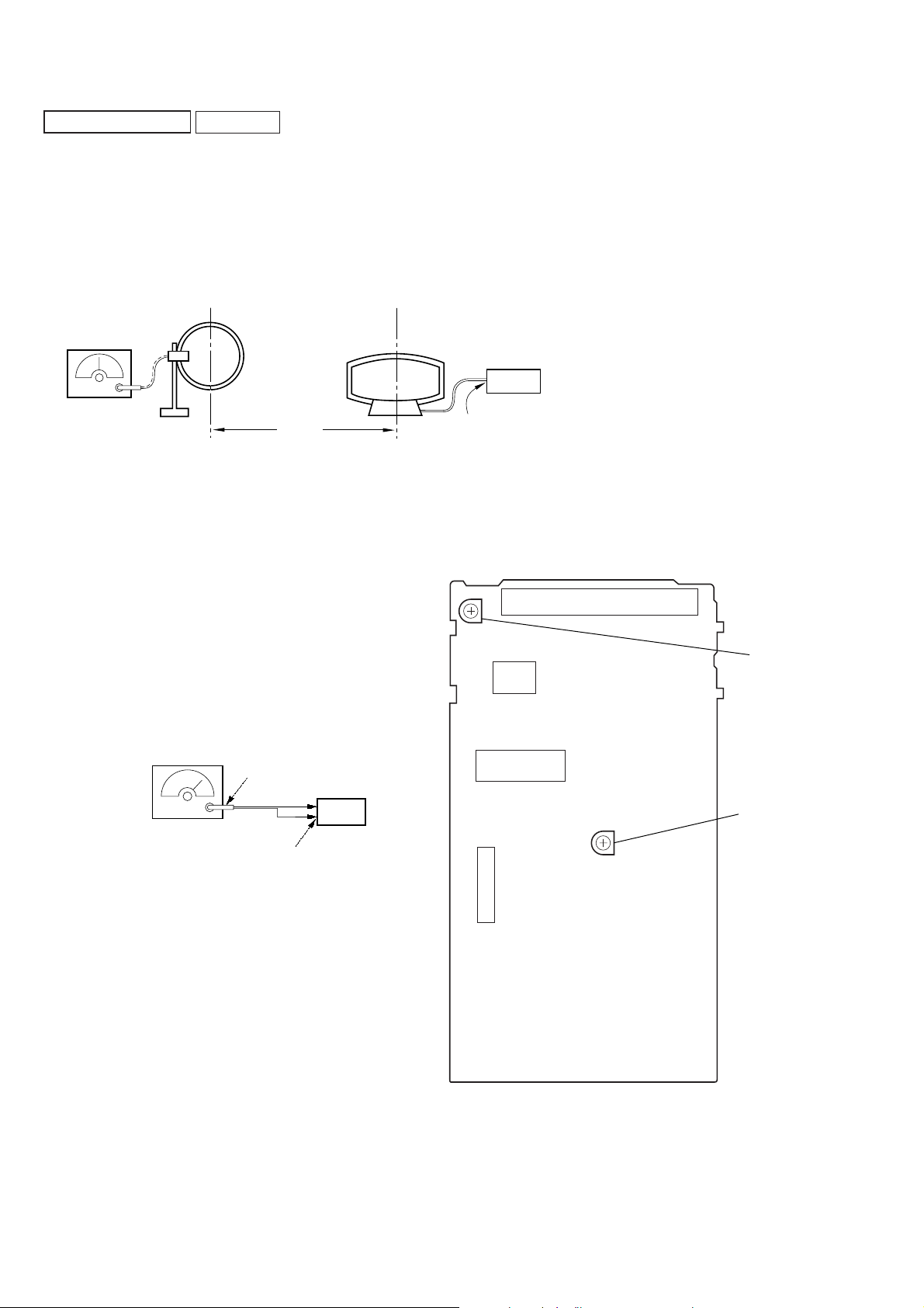
TUNER SECTION 0 dB=1 µV
(AEP, German, UK, East European, CIS models only)
Note: As a front-end (FE1) is difficult to repair if faulty, replace it with
new one.
AM Section Adjustment
Note: FM Tuned Level Adjustment should be performed after this AM
Tuned Level Adjustment.
Setting:
AM Tuned Level Adjustment
Band: MW
Procedure:
1. Set the output of SSG so that the input level of the set be-
comes 55 dB.
2. Tune the set to 999 kHz or 1,050 kHz.
3. Adjust R V41 to the point (moment) when the TUNED indica-
tor will change from going off to going on.
Adjustment Location : TCB board
FM Section Adjustment
Note: This adjustment should be performed after the AM Tuned Level
Adjustment due to the same adjustment element.
Setting:
FM Tuned Level Adjustment
Band: FM
Procedure:
1. Supply a 25 dBµ 98 MHz signal from the ANTENNA termi-
nal.
2. Tune the set to 98 MHz.
3. If the TUNED indicator does not light, adjust RV42 to the
point (moment) when the TUNED indicator will change from
going off to going on.
AM RF SSG
loop antenna
set
loop antenna
(Supplied accessories)
60 cm
AM ANTENNA
terminal (TM1)
30% amplitude
modulation by
400 Hz signal
Field strength dB (
µ
V/m) =SSG output level dB (
µ
V/m) –26 dB.
Carrier frequency : 98 MHz
Modulation : AUDIO 1 kH, 75 kHz
deviation (100%)
FM ANTENNA terminal
(TM1) (75
Ω
open)
75
Ω
coaxial
set
FM RF stereo signal
generator
Adjustment Location: TCB board
Adjustment Location:
[TCB BOARD] (Component Side)
TM1
IFT41
IC41
CN1
RV42
FM T uned
Level
Adjustment
RV4
AM T uned
Level
Adjustment
– 17 –
FM Polar Adjustment (East European, CIS models only)
Connection 1:
Connection 2:
Adjustment Location :
East European, CIS:
[TCB BOARD] (Component Side)
Procedure :
1. Set the modulation of FM RF SSG to AUDIO 1 kHz, 10 kHz
deviation according to “Connection 1”.
2. Tune the set to 69 MHZ.
3. Adjust the RV1702 so that the reading of frequency counter
connected to TP1702 becomes within 31.25 kHz ± 0.05 kHz.
(VCO Adjustment)
4. Then record the reading of the level meter connected to TP1701
5. Set the modulation of FM RF SSG to AUDIO 31.25 kHz, 10
kHz deviation according to “Connection 2”.
6. Tune the set to 69 MHz.
7. Set the CT1701 to be mechanical center.
8. Adjust the L1701 so that the reading of the level meter con-
nected to TP1701 become maximum.
Then adjust the CT1701 so that the reading of the level meter
connected to TP1701 becomes maximum. (SUB CARRIER
PEAK Adjustment)
9. Adjust the RV1701 so that the level at the moment becomes
14dB higher value than the level recorded in step 4. (SUB CAR-
RIER LEVEL Adjustment)
[TCB BOARD] (Conductor Side)
FM ANTENNA terminal
(75
Ω
)
75
Ω
coaxial
set
FM RF SSG
AF OSC
Audio 31.25 kHz
external
modulation
terminal
Carrier frequency: 69 MHz
Output level : 1mV (60 dB
µ
) (at 75
Ω
open)
Modulation : AUDIO 31.25 kHZ, 10 kHz deviation
(
EXTERNAL MODULATION
)
FM ANTENNA termina
l
(75
Ω
)
75
Ω
coaxial
set
FM RF SSG
Carrier frequency: 69 MHz
Output level : 1mV (60dB
µ
) (at 75
Ω
open)
Modulation : AUDIO 1 kHZ, 10kHz deviation
TM1
IFT41
IC41
CN1
RV42
FM T uned Level
Adjustment
RV41
AM T uned Level
Adjustment
L1701
Sub Carrier Pea
k
Adjustment
RV1701
Sub Carrier Level
Adjustment
CT1701
Sub Carrier Peak
Adjustment
RV1702
VCO Adjustment
frequency
counter
+
–
+
–
level meter
Q1701
Q1702
Q1703
TP1701
(FILTER)
TP1702
(VCO)
– 18 –
Note:
1. CD Block is basically designed to operate without adjustment. There-
fore, check each item in order given.
2. Use YEDS-18 disc (3-702-101-01) unless otherwise indicated.
3. Use an oscilloscope with more than 10 MΩ impedance.
4. Clean the object lens b y an applicator with neutral detergent when the
signal level is low than specified value with the following checks.
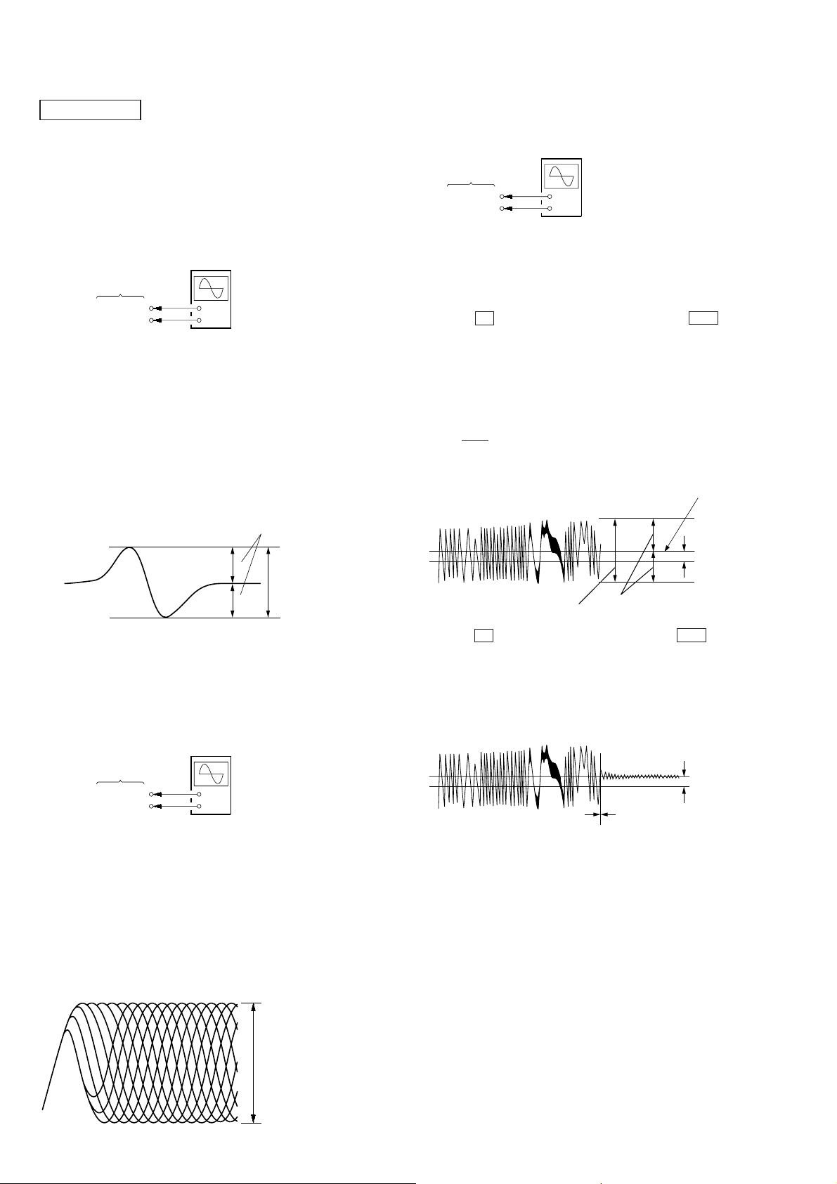
S Curve Check
Procedure:
1. Connect oscilloscope to test point TP (FEO).
2. Connect between test point TP (FOK) and GND by lead wire.
3. Turn Power switch on.
4. Put disc (YEDS-18) in and turned Power switch on again and
actuate the focus search. (Actuate the focus search when disc
table is moving in and out.)
5. Check the oscilloscope waveform (S-curve) is symmetrical
between A and B. And confirm peak to peak level within 3±1
Vp-p.
S-curve waveform
6. After check, remove the lead wire connected in step 2.
Note: • Try to measure several times to make sure than the ratio of A : B
or B : A is more than 10 : 7.
• Take sweep time as long as possible and light up the brightness
to obtain best waveform.
RF Level Check
Procedure:
1. Connect oscilloscope to test point TP (RF) on BD board.
2. Turned Power switch on.
3. Put disc (YEDS-18) in and playback.
4. Confirm that oscilloscope waveform is clear and check RF
signal level is correct or not.
Note: Clear RF signal waveform means that the shape “≈” can be clearly
distinguished at the center of the waveform.
• FR signal
E-F Balance (Traverse) check
(Without remote commander)
Procedure:
1. Connect oscilloscope to test point TP (TEO) on BD board.
2. Turned Power switch on. Press [FUNCTION] button to select
CD.
3. Put disc (YEDS-18) in to play the number five track.
4. Press the p button, [ENTER/NEXT] button and ^ but-
ton simultaneously several times to fluorescent indicator tube
display “SHUFFLE” is blink. (The sledding servo is turned
OFF.)
5. Check the level B of the oscilloscope’s waveform and the A
(DC voltage) of the center of the Traverse waveform.
Confirm the following:
Traverse waveform
6. Press the p button, [ENTER/NEXT] b utton and ^ button
simultaneously several times to fluorescent indicator tube dis-
play “SHUFFLE” is OFF. (The sleding servo is turned ON.)
Confirm the C (DC voltage) is almost equal to the A (DC v olt-
age) is step 5.
Traverse waveform
CD SECTION
A
× 100 = less than ±7 (%)
B
A
B
symmetry
within 3
±
1 Vp-p
+
–
BD board
TP (RF)
TP (VC)
oscilloscope
VOLT/DIV: 200 m
V
TIME/DIV: 500 ns
level:
1.3
±
0.3 Vp-p
+
–
BD board
TP (FEO)
TP (VC)
oscilloscope
+
–
BD board
TP (TEO)
TP (VC)
oscilloscope
A (DC
voltage)
B
0 V
level: 500
±
100 mVp-p
symmetry
Center of the waveform
C (DC
voltage
)
0 V
Sled servo ONSled servo OFF
– 19 –
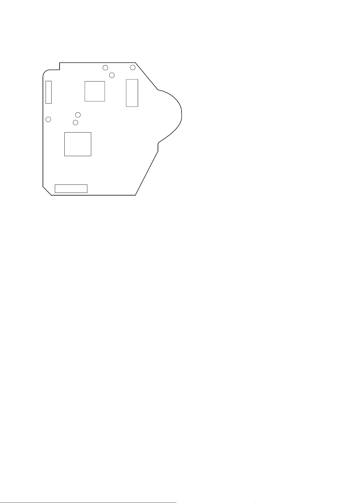
Adjustment Location:
[BD BOARD] (Conductor Side)
IC103
CNU102
IC101
IC
I02
RF
FOK
VC
FEO
TEO
GND
CNU101
– 20 –
SECTION 7
DIAGRAMS
• Circuit Boards Location
SENSOR board
MOTOR (TURN) board
MOTOR (SLIDE) board
BD board
LEAF SW board
AUDIO board
CONNECTOR board
TRANSFORMER board
CD-SW board
PANEL board
HP board
POWER AMP board
MAIN board
ENCAPSULATED COMPONENT
(GRX7/GRX7J: Saudi Arabia/RX77: Canadian)
TCB board
(AEP, UK, German, East European, CIS)
TUNER
(Tourist)
HCD-GRX7/GRX7J/R700/RX77/RX77S
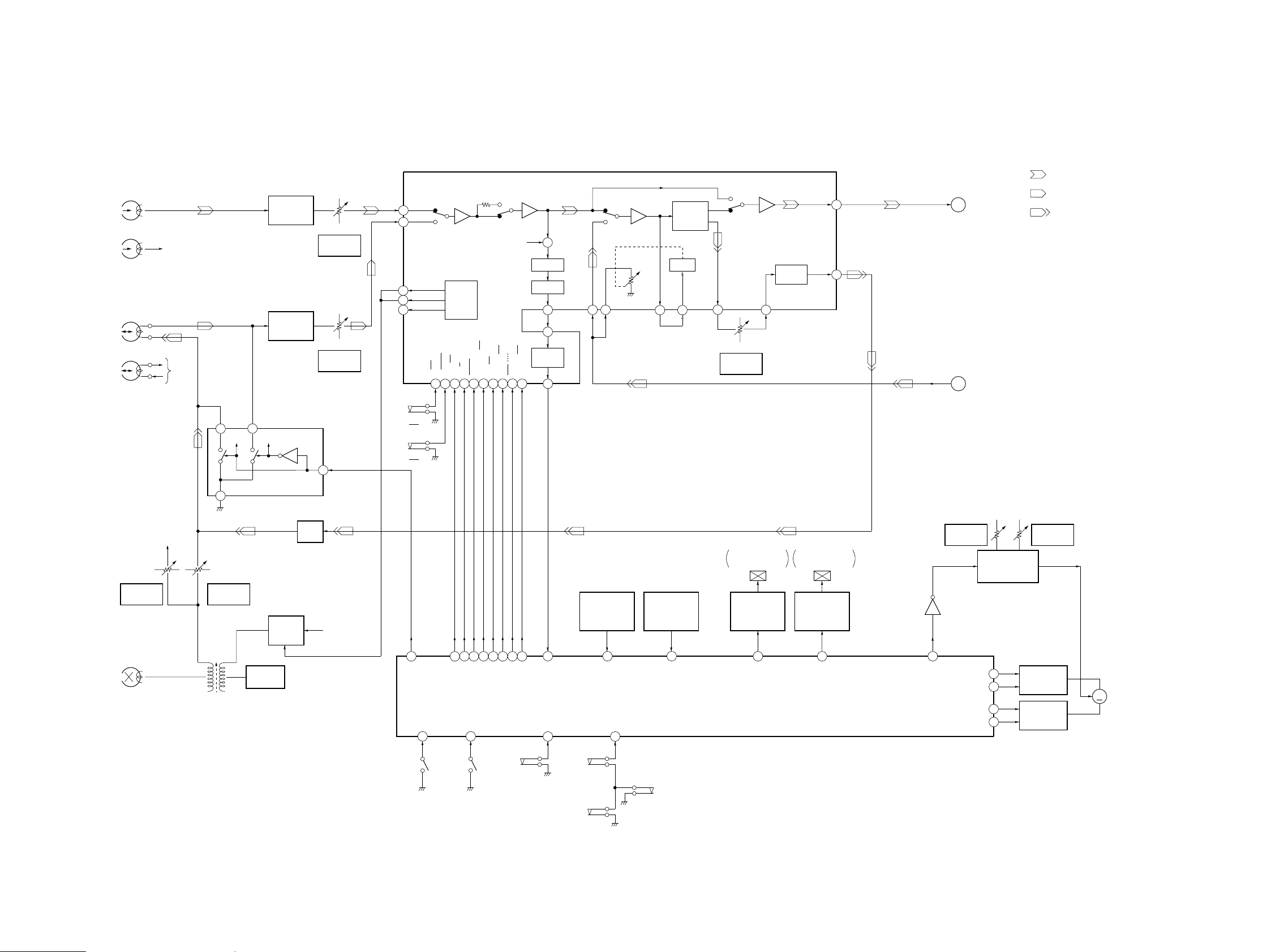
7-1. BLOCK DIAGRAM – TUNER Section (AEP, UK, German models only) –
– 21 –
– 22 –
TM1
ANTENNA
FM 75Ω
COAXIAL
ANT IN
ST +10V
Q5
B+ SWITCH
VT
FM CIRCUIT B+
FE1
FM FRONT-END
IF OUT
+B
CF1
10.7MHz
FM IF AMP
Q1, 2
CF2
10.7MHz
CF3
10.7MHz
FM-IN
REG
FM/AM IF AMP,
AM RF AMP/MIX/OSC,
FM/AM DET, MPX
IC41
05
FM/AM PLL
IC21
FM TUNED
LEVEL
RV42
X42
450kHz
D41
FM SD
AM/FM
VCO-STOP
IF-BUFF MUTE
AM-SD
ADJ
AM SD
AM TUNED
LEVEL
RV41
AM IF
IFT41
AM
IF
AM
DET
OUT
FM DET
STEREO
TUNED
X41
10.7MHz
MUTE
STEREO
STEREO, TUNED, MUTE,
ST-CE, ST-DOUT, ST-CLK, ST-DIN
TUNED
FM DET-OUT
MPX
IN
OUT L
OUT R
LPF41
L.P.F.
R-CH
AMP
IN L
AMP
OUT L
ST-L
ST-CE
ST-DOUT
ST-CLK
ST-DIN
CE
DI
CL
DO
X21
4.5MHz
AM-MIX
Q9
LW SWITCH
FE2
MW/LW FRONT-END
Q11
MW
SWITCH
Q12
MW
SWITCH
Q14
LW SWITCH
Q13
MW
SWITCH
AM-OSC
AM-RF IN
RDS DATA
RDS INT
FM
VT1
MW
MW
AM OSC
FM
VCO STOP
FM/AM IF
XIN
XOUT
RDS SIGNAL BUFFER
IC1751
RDS DECODER
IC1752
X1751
4.332MHz
5
7
MUX
DATA
INT
OSCI
OSCO
AM
1
5
7
1
6
14
13
15
16
17
29
27
30
14 15 13
4
24
7
6
2
5
3
2
10
17
9 11
14
7
2
12
IF REQ
8
1
24
4
3
6
5
26 25
24
23
22
21
20
6
FM IF AMP
Q3, 4
12
23
22
4
13
14
2
16
21
19
17
20
28
10
12
9
(Page 29)
I
(Page 29)
K
(Page 29)
J
• SIGNAL PATH
: FM
: AM (MW/LW)
HCD-GRX7/GRX7J/R700/RX77/RX77S
– 23 –
– 24 –
7-2. BLOCK DIAGRAM – TUNER Section (East European, CIS models only) –
TM1
ANTENNA
FM 75Ω
COAXIAL
ANT IN
ST +10V
Q5
B+ SWITCH
VT
FM CIRCUIT B+
FE1
FM FRONT-END
IF OUT
+B
CF1
10.7MHz
FM IF AMP
Q1 – 4
CF3
10.7MHz
FM-IN
REG
FM/AM IF AMP,
AM RF AMP/MIX/OSC,
FM/AM DET, MPX
IC41
05
FM/AM PLL
IC21
FM TUNED
LEVEL
RV42
X42
450kHz
D41
D42
D43
FM SD
AM/FM
VCO-STOP
IF-BUFF MUTE
AM-SD
ADJ
AM
SD
AM TUNED
LEVEL
RV41
RV1702
VCO
TP1702, RV1702
SUB CARRIER
LEVEL
RV1701
SUB CARRIER
PEAK
CT1701, L1701, TP1701
SWITCHING
Q1702
SWITCHING
Q1703
SWITCHING
Q1701
AM IF
IFT41
AM
IF
AM
DET
OUT
FM DET
STEREO
TUNED
X41
10.7MHz
MUTE
STEREO
STEREO, TUNED, MUTE,
ST-CE, ST-DOUT, ST-CLK, ST-DIN
TUNED
FM DET-OUT
MPX
IN
OUT L
OUT R
LPF41
L.P.F.
AMP
IN L
AMP
OUT L
ST-L
ST-CE
ST-DOUT
ST-CLK
ST-DIN
CE
DI
CL
DO
X21
4.5MHz
AM-MIX
Q9
LW SWITCH
FE2
MW/LW FRONT-END
Q11
MW
SWITCH
Q12
MW
SWITCH
Q14
LW SWITCH
Q13
MW
SWITCH
AM-OSC
AM-RF IN
FM
VT1
MW
MW
AM OSC
FM
VCO STOP
FM/AM IF
IF REQ
XIN
XOUT
POLAR DECODER
IC1701
IN
SUB IN
SUB IN
L OUT
R OUT
MON
TP1702
TP1701
L1701
CT1701
R-CH
VCO
AM
8
4
1
1
6
14
13
15
16
17
29
27
30
14 15 13
4
24
7
6
2
5
3
2
10
17
9 11
14
7
2
12
8
1
24
FM LOW
13
4
3
6
5
26 25
24
23
22
21
20
5
12
23
22
2
20
18
7
6
VCO STOP
9
ST IND
10
21
19
17
20
28
D1704
D1701
D1702
D1703
10
12
9
(Page 29)
I
(Page 29)
J
• SIGNAL PATH
: FM
: AM (MW/LW)
3
13
12
5
3
9
11
4
14
CA
POLAR /PILOT SWITCH
IC1702
17
HCD-GRX7/GRX7J/R700/RX77/RX77S
– 25 – – 26 –
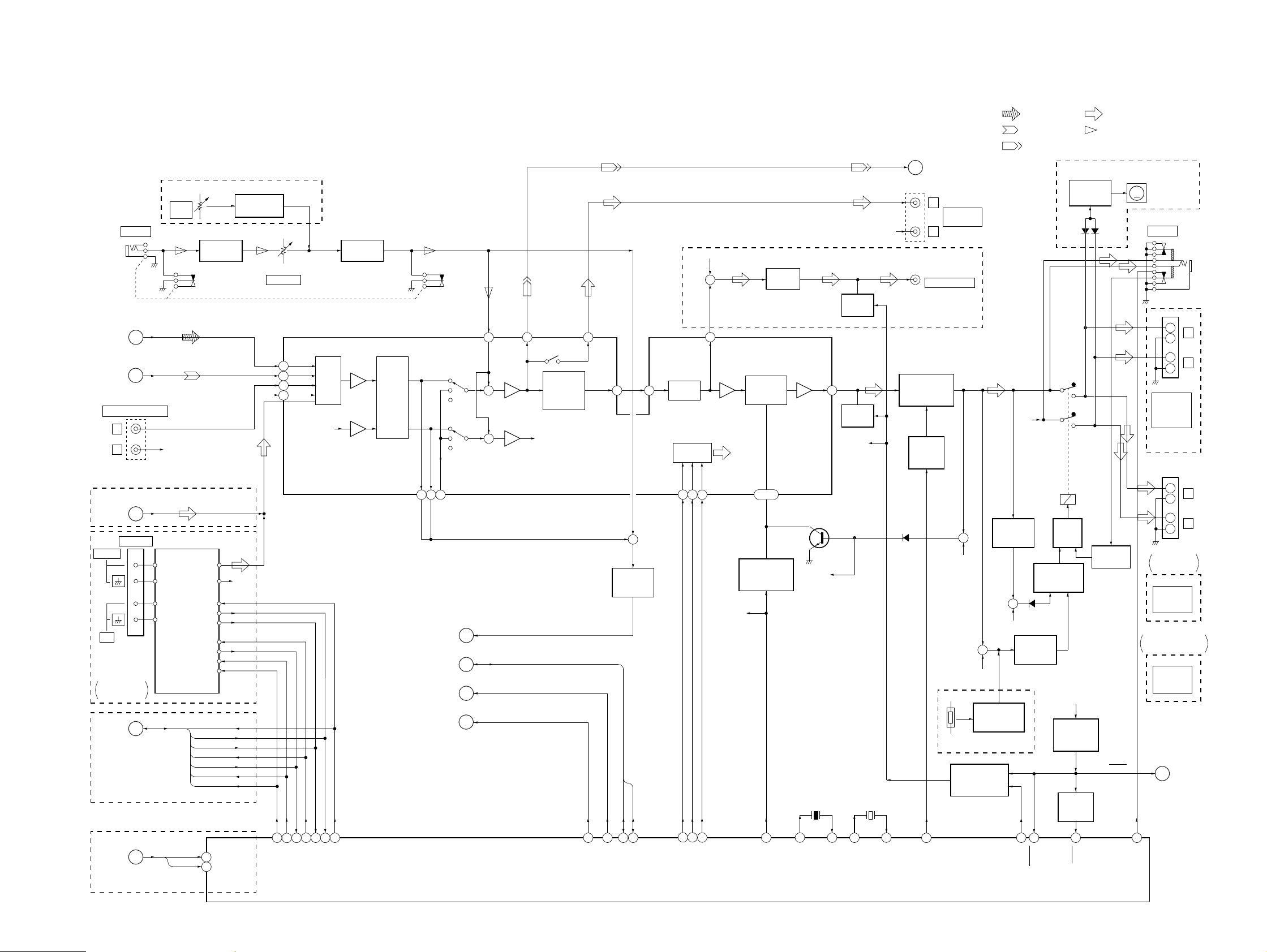
7-3. BLOCK DIAGRAM – CD MECHANISM DECK Section –
XROF
M
M
A
B
D
F
E
C
I-V AMP
DETECTOR
39
1
2
10
6
5
4
38
16
15
18
17
12
OUT2A
OUT2B
SLO
OUT3B
OUT3A
OUT4A
OUT4B
SPINDLE
MOTOR DRIVE
M101
(SPINDLE)
SLED
MOTOR DRIVE
11
M102
(SLED)
FOCUS
COIL DRIVE
BUFFER
OUT1A
OUT1B
3
6
27
9
26
24
IN3B
IN4A
MUTE
IN2A
IN1B
SLP
FOCUS/TRACKING COIL DRIVE,
SPINDLE/SLED MOTOR DRIVE
IC102
16
14
SLED
AMP
LD
PD
LASER DIODE
OPTICAL PICK-UP
(KSS-213D/Q-NP)
2-AXIS
DEVICE
(FOCUS)
(TRACKING)
33
32
27
44
23
22
20
21
19
23
RF AMP,
FOCUS/TRACKING
SERVO
IC101 (1/2)
FOCUS OK
COMPARATOR
MIRR
AMP
DEFECT
AMP
FOCUS OK
AMP
IIL DATA REGISTER
4038
FILTER
42
39
FILO
PCO
CLTV
FILI
DIGITAL PLL
ASYMMETRY
CORRECTION
EFM
DEMODULATOR
SERIAL
INPUT
INTERFACE
OVER
SAMPLING
DIGITAL
FILTER
NOISE
SHAPER
PWM &
INTEGRATOR
BUFFER
ERROR
CORRECTOR
16K
RAM
SUB-CODE
PROCESSOR
SERVO AUTO SEQUENCER
DIGITAL CLV
17
15
52
54
50
100
16
LRCKI
BCKI
8 7
9
10
12
11
75
76
77
26
28
14
13
TBL-L
TBL-R
S101
(LIMIT)
M
3
6
7
2
MOTOR
DRIVE
DISC TRAY TURN MOTOR DRIVE
IC701
OUT1
OUT2
IN1
IN2
M701
(DISC TRAY TURN)
41
42
36
37
1
40
45
2
47
13
14
6
25
24
13
+
PD1
PD1 I-V AMP
RFO
RF
46
ASYI
47
ASYO
FOK
DATO
CLKO
XLTO
SEIN
CNIN
SQ-DATA-IN
SQ-CLK (D-OUT ON/OFF)
SENS
CD-DATA
CD-CLK
XLT
SCOR
MON
MDP
MDS
29
LOCK
64
SQSO
SQCK
SENS
DATA
CLOK
XLAT
SCOR
SBSO
EXCK
SPOD
GFS
EMPH
WFCK
GTOP
X101
16.9344MHz
RFI
FOK
DATA
CLK
SENS1
26
SENS2
C.OUT
XLT
LOCK
XRST
PD2 I-V AMP
PD2
TTL
IIL
FEO
TEO
PD
FEI
FEO
TAO
TEI
TTL
IIL
TTL
IIL
FOCUS
ERROR
AMP
RF
SUMMING
AMP
TRACKING
ERROR
AMP
TRACKING PHASE
COMPENSATION
FOCUS PHASE
COMPENSATION
AUTOMATIC
POWER CONTROL
Q101
I-V
AMP
LD
AMP
PD
AMP
FE BIAS
F
E
LD
89
XRST
XTAI
90
XTAO
70
C4M
CKO
PCMD
BCK
LRCK
63
C2PO
62
49
RFCK
WDCK
PCMDI
XRST
SLED SERVO
IC101 (2/2)
05
DIGITAL SIGNAL PROCESSOR,
CLV SERVO PROCESSOR,
DIGITAL FILTER, D/A CONVERTER
IC103
SYSTEM CONTROLLER
IC501 (1/3)
ON : When the optical pick-up
is inner position.
• SIGNAL PATH
(Page 29)
: CD PLAY
: DIGITAL OUT
27
CPU INTERFACE
D/A
INTERFACE
CLOCK
GENERATOR
OPTICAL
TRANSCEIVER
IC381
LEVEL SHIFT
Q701
DISC SENSOR
IC703
IC381
CD DIGITAL
OUT
OPTICAL
TIMING
LOGIC
74
58
DOUT
71
53
55
51
EMPHI
AOUT1
AOUT2
LOUT1
LOUT2
R-CH
AIN1
AIN2
CD-L
SENS2
73
34
36
74
47
48
58
18
DISC TRAY SENSOR
IC702
ROTARY
ENCODER
S811
DISC-SENS
OUT-OPEN
S801
(OPEN/CLOSE DET)
ENC1
ENC2
ENC3
57
A
75
TBL-SENS
76
4
80
TRACKING
COIL DRIVE
OP
OUT
OP+,
OP–
22, 23
6
INTERNAL BUS
DIGITAL
OUT
61
72
73
84 95
85
94
86
93
CLOSE
OPEN
81
79
78
2
3
21
60
61
LOAD-OUT
LOAD-IN
M
10
2
7
4
MOTOR
DRIVE
DISC TRAY SLIDE MOTOR DRIVE
IC801
OUT1
OUT2
FIN
RIN
M801
(DISC TRAY SLIDE)
63
64
HCD-GRX7/GRX7J/R700/RX77/RX77S
– 27 –
– 28 –
7-4. BLOCK DIAGRAM – TAPE DECK Section –
PB EQ AMP
(DECK A)
IC611
PB LEVEL (L)
(DECK A)
REC-L
PB-L
CAPSTAN MOTOR
CONTROL SWITCH
Q1001
CAPSTAN
MOTOR DRIVE
Q336 – 339
1
B
(Page 29)
(Page 30)
L-CH
R-CH R-CH
HRP1
(PLAYBACK)
PB EQ AMP
(DECK B)
IC601
L-CH
R-CH R-CH
05
R-CH
R-CH
HRP2 (1/2)
(RECORD/PLAYBACK)
ALC
REC
EQ AMP
AMS
CIRCUIT
DOLBY NR
AMP
CIRCUIT
BIAS
CONTROL
CIRCUIT
DOLBY PASS
R-CH
L.P.F.
BUFFER
Q335
M
M1
(CAPSTAN)
HRP2 (2/2)
(ERASE)
BIAS OSC
T621
B+
(A+7V)
R-CH
3
46
28
43
36
40
35 34
39
26
31
19
15
16
18
20
22 23
24
2517
99
94
93
92
90 89
88
87
31
33
32
+
48
4
2
RV311
PB LEVEL (L)
(DECK B)
RV301
TAPE SPEED
(NORMAL)
RV1002
TAPE SPEED
(HIGH)
RV1001
REC LEVEL (L)
(DECK B)
RV301
REC BIAS (R)
(DECK B)
RV441
REC BIAS (L)
(DECK B)
BIAS OSC
Q621, 622
REC BIAS
SWITCH
Q623
ROTATION
DETECT SENSOR
(DECK A)
IC1001
RV341
BIAS
TRAP
C331, L331
REC/PB SWITCHING
IC602
SYSTEM CONTROLLER
IC501 (2/3)
DECK PROCESS
DECK A/B SELECT, PB/REC EQ AMP,
DOLBY NR AMP, ALC, AMS
IC301
AIN (L)
BIN (L)
MAOUT
PB OUT (L)
EQ OUT
(L)
MSIN
MSOUT
BIAS ON/OFF
70
120
BIAS (N)
BIAS (C)
BIAS (M)
S1004
A 120/70
B NORM/CROM
ALC ON/OFF
PB A/B
NORM/HIGH
NR ON/OFF
RM ON/OFF
REC/PB/PASS
LM ON/OFF
(DECK A 120/70)
98
S1003
S1001
(DECK A PLAY)
S1002
(DECK B PLAY)
(DECK A HALF)
S1008
(DECK B 120/70)
27
REC OUT (L)
ROUT (L)
RIN (L)
ALC (L)
EQ IN (L)
ALC
IN (L)
44
38
97
AMS-IN
26
A-SHUT
ROTATION
DETECT SENSOR
(DECK B)
IC1002
27
B-SHUT
TRIGGER
PLUNGER DRIVE
(DECK A)
Q333, 334
84
A-TRG
TC-MUTE
R/P-PASS
NR-ON/OFF
REC-MUTE
BIAS
EQ-H/N
PB-A/B
ALC-ON/OFF
TC-RELAY
A-PLAY-SW
B-PLAY-SW
A-HALF
28
S1006
(DECK B HALF)
S1009
(DECK B REC)
S1005
(DECK A REC)
B-HALF
SL1
TRIGGER PLUNGER
DECK A
TRIGGER
PLUNGER DRIVE
(DECK B)
Q331, 332
83
B-TRG
82
17
77
CAP-M-H/L
CAPM-CNT1P
CAPM-CNT2P
CAPSTAN
MOTOR DRIVE
Q340 – 343
85
86
CAPM-CNT1M
CAPM-CNT2M
SL2
TRIGGER PLUNGER
DECK B
95 96
C
• SIGNAL PATH
: PLAYBACK (DECK A)
: PLAYBACK (DECK B)
: RECORD
HCD-GRX7/GRX7J/R700/RX77/RX77S
– 29 –
– 30 –
7-5. BLOCK DIAGRAM – MAIN Section –
MIC LEVEL
DBFB CONTROL
SWITCH
Q111
SPEANA
MIXING AMP
IC102
RESET SIGNAL
GENERATOR
IC502
POWER AMP
IC801
CD-L
A
(Page 26)
(Page 28)
C
(Page 28)
PB-L
B
ST-L
I
(Page 22, 24)
J
(Page 22, 24)
K
(Page 22)
R-CH
R-CH
05
FM/AM TUNER UNIT
VOLUME
CONTROL
CPU
INTERFACE
BASS BOOST
CONTROL
CIRCUIT
INPUT
SELECT
SOUND
CONTROL
CIRCUIT
GRAPHIC
EQUALIZER
CONTROL
CIRCUIT
67
R-CH
FEED BACK SWITCH
Q112
R-CH
R-CH
COMMAND
F OUT2
BUF
OUT2
VOL
IN2
+
R-CH
R-CH
D141
D403
D404
M401
(FAN MOTOR)
R-CH
+
+
+
68
2
58
RV750
ECHO
LEVEL
RV751
MIC AMP
IC750 (2/2)
DIGITAL ECHO
IC751
MUTING
Q113
LINE AMP
IC191
OVER LOAD
DETECT
Q801
OVER LOAD
DETECT SWITCH
Q432, 437
DC DETECT
SWITCH
Q433, 434
TEMPERATURE
DETECT SWITCH
Q831, 832
RESET
SWITCH
Q501
RELAY
DRIVE
Q431
PROTECTOR
Q435, 436
GRAPHIC EQUALIZER CONTROL,
ELECTRICAL VOLUME
IC101
IN B2
IN C2
66
60 5
69
IN A2
IN D2
KEY IN2
KEY IN1
75
33 32
34
KEY OUT
DATA
CLOCK
LATCH
52 51
3
M62442-DATA
M62442-CLK
M62442-LATCH
10
X2
X501
5MHz
X502
32.768kHz
11
X1
13
XT2
14
XT1
BB B2,
BB A2
MIC IN
VOL OUT2
REC
A2
REC-L
E
(Page 31)
D
(Page 31)
(Page 31)
(Page 32)
(Page 32)
SPEANA
DATA, CLK
POWER
CD-POWER
REC
B2
• SIGNAL PATH
: CD PLAY
: TAPE PLAY
: RECORD
: TUNER (FM/AM)
: MIC INPUT
R-CH
TH831
+5V
+
R-CH
R-CH
-1
-2
+
+
–
–
+
MUTING
Q191
R-CH
R-CH
57
42
STANDBY
SWITCH
Q575
MUTING CONTROL
SWITCH
Q571, 572
41
100
2
16
15
6
36
40
J101 (2/2)
MD/VIDEO
(AUDIO) OUT
J191
SUPER WOOFER
J421
PHONES
R
L
TM402
SURROUND
SPEAKER
IMPEDANCE
USE 16Ω
TM401
TM401
SPEAKER
IMPEDANCE
USE 8 – 16Ω
R
L
J101 (1/2)
J751
R
MIX MIC
MD/VIDEO (AUDIO) IN
L
ST-L
FM ANT
FM ANT
AM ANT
AM ANT
ST-R
ST-MUTE
STEREO
TUNED
ST-DIN
ST-DOUT
ST-CLK
ST-CE
ANTENNA
FM 75Ω
AM
38, 39
D843
RY401
+
–
–
+
R
L
DBFB-H/L
CD-POWER
POWER
IIC-CLK
IIC-DATA
CLK
DATA
68
21
22
ST-CE
65
ST-CLK
66
ST-DIN
67
ST-DOUT
69
TUNED
70
STEREO
72
ST-MUTE
ST-CE
RDS-DATA
RDS-INT
RDS DATA,
RDS INT
ST-CLK
ST-DIN
ST-DOUT
TUNED
STEREO
ST-MUTE
(AEP, UK, German, East European, CIS models)
(AEP, UK, German models)
(AEP, UK, German, East European, CIS models)
STK-MUTE
LINE-MUTE
F-RELAY
AC-CUT
RESET
1
RESET
SYSTEM CONTROLLER
IC501 (3/3)
5655
F
G
H
46 5
+
GRX7/GRX7J/
RX77: Canadian
(Canadian model)
GRX7/GRX7J/
RX77: Canadian
TM401
SPEAKER
IMPEDANCE
USE 6 – 16Ω
AEP, UK, German, East
European, CIS models
(GRX7/GRX7J/RX77: Canadian)
(GRX7/GRX7J/RX77: Canadian)
(GRX7/GRX7J/RX77: Canadian)
MIC AMP
IC750 (1/2)
(Saudi Arabia model)
M
FAN MOTOR
DRIVE
Q401, 402
HCD-GRX7/GRX7J/R700/RX77/RX77S
– 31 –
– 32 –
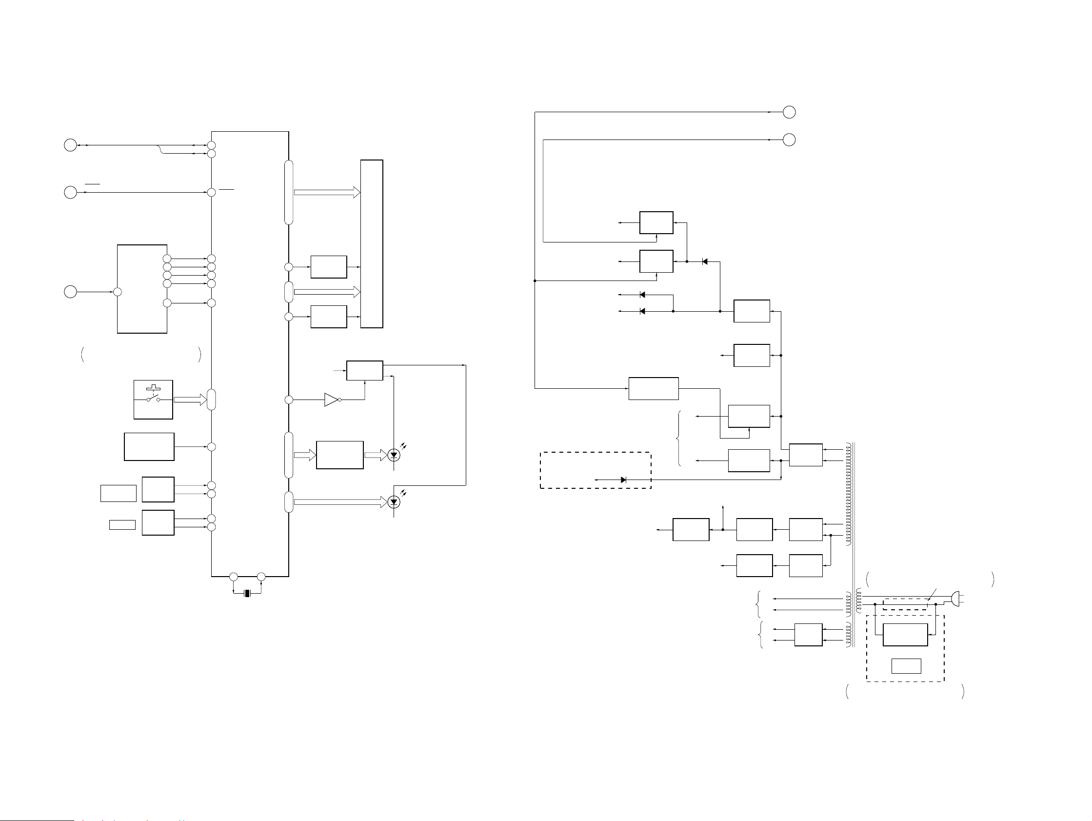
7-6. BLOCK DIAGRAM – DISPLAY/KEY CONTROL/POWER SUPPLY Section –
REGULATOR
CONTROL SWITCH
Q903
D914
D501, 502
D507
POWER
(Page 29)
G
CD-POWER
(Page 29)
H
D405 – 407
D+5V
AUDIO D+5V
B+
SWITCH
Q905, 906
–30V
REGULATOR
Q910
–30V
FL DRIVER (IC601)
CAPSTAN MOTOR DRIVE CIRCUIT,
TRIGGER PLUNGER DRIVE CIRCUIT B+
RECT
D909, 910
+12V
REGULATOR
IC903
+10V
REGULATOR
Q909
–7V
REGULATOR
Q914, 951, 952
+7V
REGULATOR
Q901, 902, 913
+10V
(FM/AM TUNER CIRCUIT B+)
+7V
REGULATOR
IC901
+7V
(CD M+7V)
+5V
REGULATOR
IC902
CD MECHANISM DECK
SECTION B+
B+
SWITCH
Q907, 908
SYSTEM CONTROLLER
(IC501) B+
RECT
D907, 908
RECT
D901 – 904
RECT
D800
VOLTAGE
SELECT SWITCH
S11
VOLTAGE
SELECTOR
S11
AC IN
B+
POWER AMP
(IC801)
POWER TRANSFORMER
T11
B–
+7V
TC, PANEL, AUDIO
–7V
FAN MOTOR B–
VF1
TO
FLUORESCENT INDICATOR TUBE
(FL601)
VF2
REMOTE CONTROL
RECEIVER
IC602
GRID DRIVE
Q621
FLUORESCENT INDICATOR TUBE DRIVE,
LED DRIVE, KEY CONTROL
IC601
FLUORESCENT
INDICATOR TUBE
FL601
BAND-PASS FILTER
IC603
Q603
D+5V
SPEANA-1
36
SPEANA-3
37
SPEANA-4
GRID DRIVE
Q620
32
L+R
LINE IN
33
SIRCS
ROTARY
ENCODER
S601
ROTARY
ENCODER
S602
21
JOG-A
19
VOL-A
22
JOG-B
20
8
9
VOL-B
X-OUT
X-IN
B+ SWITCH
Q601, 602
LED DRIVE
Q604, 607 – 610,
Q613 – 615, 618
KEY-0 – KEY-3
SPEANA-2
F01
F03
F04
L+R
F02
GR1
(Page 30)
(Page 29)
D
DATA, CLK
(Page 29)
D610, 612, 620 – 625,
D631 – 633, 651, 652
D613 – 618
SPEANA
41
L.SEL
25
GR13
53
SDA
SCL
DATA
CLK
RESET
RESET
35
23
24
10
34
15
14
4
13
16
17
26 – 29
SEG1 – SEG24
54 – 69, 72 – 70, 77 – 73
GR2 – GR12
42 – 52
LED1, LED5 – LED8,
LED12 – LED15
79, 3 – 6, 15 – 18
LED9, LED10
11, 12
S601
(JOG DIAL)
S604 – 625, 631 – 642,
S655 – 659
S602
05
= ↔ +
DJ MIX
VOLUME
X601
8MHz
E
F
S611 – 613; GRX7/GRX7J/RX77: Canadian only,
S655; AEP, UK, German models only
E, Saudi Arabia, Malaysia, Singapore, Indonesia,
Hon
g
Kon
g
, Taiwan, South African models
Except E, Saudi Arabia, Malaysia, Singapore,
Indonesia, Hong Kong, Taiwan, South African models
(D620, Q607; GRX7/GRX7J/RX77: Canadian only)
(GRX7/GRX7J/RX77: Canadian)
HCD-GRX7/GRX7J/R700/RX77/RX77S
– 33 –
– 34 –
Note on Schematic Diagram:
• All capacitors are in µF unless otherwise noted. pF: µµF
50 WV or less are not indicated except for electrolytics
and tantalums.
• All resistors are in Ω and
1
/
4
W or less unless otherwise
specified.
•
¢
: internal component.
• C : panel designation.
Note on Printed Wiring Boards:
• X : parts extracted from the component side.
• p : parts mounted on the conductor side.
•
®
: Through hole.
• b : Pattern from the side which enables seeing.
(The other layers' patterns are not indicated.)
Note:
The components identi-
fied by mark ! or dotted
line with mark ! are criti-
cal for safety.
Replace only with part
number specified.
Note:
Les composants identifiés par
une marque ! sont critiques
pour la sécurité.
Ne les remplacer que par une
piéce portant le numéro
spécifié.
Caution:
Pattern face side: Parts on the pattern face side seen from
(Side B) the pattern face are indicated.
Parts face side: Parts on the parts face side seen from
(Side A) the parts face are indicated.
• U : B+ Line.
• V : B– Line.
• H : adjustment for repair.
• Voltages and waveforms are dc with respect to ground
under no-signal (detuned) conditions.
• V oltages are taken with a VOM (Input impedance 10 MΩ).
Voltage var iations may be noted due to normal produc-
tion tolerances.
• Waveforms are taken with a oscilloscope.
Voltage var iations may be noted due to normal produc-
tion tolerances.
• Circled numbers refer to waveforms.
• Signal path.
F : FM
f : AM
E : PB (DECK A)
d : PB (DECK B)
G : REC (DECK B)
J : CD
c : digital out
N : Mic in
• Abbreviation
AUS : Australian model.
CND : Canadian model.
E2 : 120 V AC Area in E model.
E3 : 240 V AC Area in E model.
EA3 : Saudi Arabia model.
EA4 : Israel model.
EE : East European model.
G : German model.
HK : Hong Kong model.
IA : Indonesian model.
JE : Tourist model.
MX : Mexican model.
MY : Malaysia model.
SAF : South African model.
SP : Singapore model.
TH : Thai model.
TW : Taiwan model.
THIS NOTE IS COMMON FOR PRINTED WIRING BOARDS AND SCHEMATIC DIAGRAMS.
(In addition to this, the necessary note is printed in each block.)
– MAIN Section –
4.4 Vp-p
200 ns
2 IC501 !¢ (XT1)
2.2 Vp-p
30.6
µ
s
– PANEL Section –
3 IC601 9 (X-IN)
3.6 Vp-p
126 ns
C
B
These are omitted.
E
Q
• Indication of transistor.
B
These are omitted.
CE
Q
5 Vp-p
230
µ
s
0.5 Vp-p
2 IC101 2 (FEI) (PLAY MODE)
5 IC103 ^º (XPCK)
4 IC103 @¶ (MDP)
2.5 Vp-p
7.8
µ
s
0.2 Vp-p
3 IC101 $¶ (TEI) (PLAY MODE)
1.3 Vp-p
6 IC103 ^™ (RFCK)
5 Vp-p
135
µ
s
5 Vp-p
135
µ
s
7 IC103 &¢ (WFCK)
8 IC103 *ª (XTAI)
2.6 Vp-p
16.9344 MHz
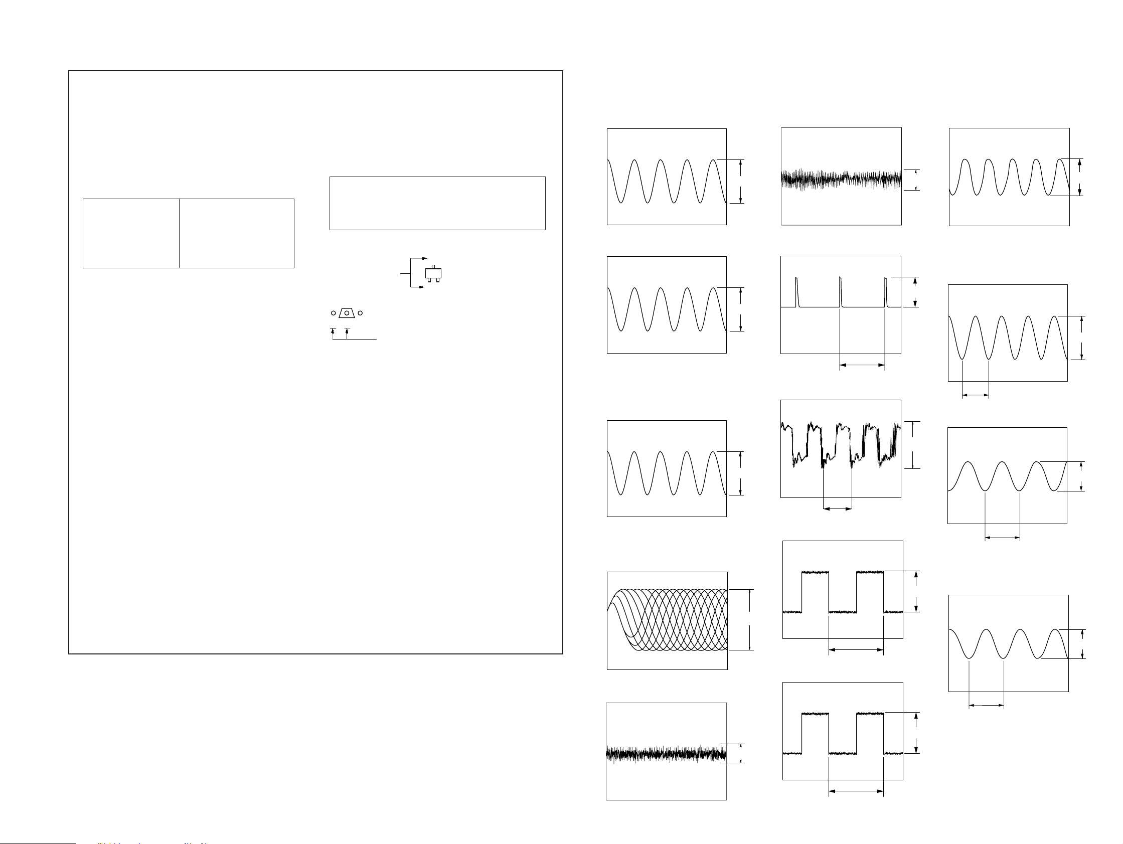
• Wavef orms
– TUNER Section –
(AEP, UK, German)
1 IC21 @¢ (XOUT)
1 IC501 !¡ (X1)
– CD Section –
1 IC101 #£ (RF O) (PLAY MODE)
4.2 Vp-p
4.5 MHz
2 IC1752 !¢ (OEC0)
2 Vp-p
4.332 MHz
– TUNER Section –
(East European, CIS)
1 IC21 @¢ (XOUT)
4.2 Vp-p
4.5 MHz
Loading...