


 Loading...
HCD-LV80
SERVICE MANUAL
E Model
HCD-LV80 is the tuner, deck, CD and amplifier section in LBT-LV80.
|
|
Model Name Using Similar Mechanism |
HCD-VR50/VR70 |
CD |
|
|
|
CD Mechanism Type |
CDM37L-5BD34L |
||
SECTION |
|
|
|
|
Base Unit Type |
BU-5BD34L |
|
|
|
||
|
|
|
|
|
|
Optical Pick-up Type |
KSS-213D/Q-NP |
|
|
|
|
TAPE DECK |
Model Name Using Similar Mechanism |
NEW |
|
SECTION |
|
Tape Transport Mechanism Type |
TCM-230PWR12 |
|
|
||
|
|
|
|
Amplifier section
The following measured at AC 120/220/240 V, 50/60 Hz
DIN power output (Rated)
240 + 240 watts
(4 ohms at 1 kHz, DIN) Continuous RMS power output (Reference)
300 + 300 watts
(4 ohms at 1 kHz, 10 % THD)
sensitivity 3 mV, impedance 47 kilohms sensitivity 1 mV, impedance 10 kilohms
VIDEO 1 IN (phono jacks):sensitivity 250 mV, impedance 47 kilohms
VIDEO 2 IN (phono jacks):sensitivity 250 mV, impedance 47 kilohms
MD IN (phono jacks): sensitivity 450 mV, impedance 47 kilohms
Outputs
PHONES (stereo phone jack):
accepts headphones of 8 ohms or more
VIDEO OUT (phono jack): voltage 250 mV, impedance 1 kilohm
MD OUT (phono jacks): voltage 250 mV, impedance 1 kilohm
SPECIFICATIONS
FRONT SPEAKER :
accepts impedance of 4 to 16 ohms
Video section
Inputs
VIDEO1 IN (phono jacks): 1 V p-p, 75 ohms VIDEO2 IN (phono jacks): 1 V p-p, 75 ohms
Outputs
VIDEO OUT (phono jack): 1 V p-p, 75 ohms S-VIDEO OUT (4-pin/mini-DIN jack):
Y: 1 V p-p, unbalanced, Sync negative,
C: 0.286 V p-p,
load impedance 75 ohms
VIDEO CD/CD player |
section |
|
System |
Compact disc, digital |
|
|
audio and video system |
|
Laser |
Semiconductor |
laser |
|
(λ = 780 ohm), Emission |
|
|
duration : continuous |
|
Laser output |
Max. 44.6 µW* |
|
|
* This output |
is the value |
|
measured at a distance of |
|
|
200 mm from the |
|
|
objective lens surface on |
|
|
the Optical Pick-up Block |
|
|
with 7 mm aperture. |
|
Wavelength |
780 - 790 nm |
|
Frequency Response |
2 Hz - 20 kHz (±0.5 dB) |
|
Signal-to-noise ratio |
More than 90 dB |
|
Dynamic range |
More than 90 dB |
|
CD DIGITAL OUT |
|
|
(square optical connector |
jack, rear panel) |
|
Video |
color system format |
|
|
|
NTSC, PAL |
Wave |
length: |
660 nm |
Output |
level: |
–18 dBm |
Tape player section
Recording system 4-track 2-channel stereo Frequency Response (DOLBY NR OFF)
40 - 13,000 Hz (±3 dB), using a Sony TYPE I cassette
40 - 14,000 Hz (±3 dB), using a Sony TYPE II cassette
— Continued on next page —
COMPACT Hi-Fi STEREO SYSTEM
1
Tuner section
FM Stereo, FM/AM superheterodyne tuner
FM tuner section |
|
|
Tuning range |
87.5 |
- 108.0 MHz (50 kHz |
|
step) |
|
Antenna: |
FM Wire antenna |
|
Antenna terminals |
75 ohm unbalanced |
|
Intermediate frequency |
10.7 |
MHz |
AM tuner |
section |
|
|
|
|
Tuning |
range |
|
|
|
|
Middle |
Eastern models: |
531 - 1,602 kHz (with |
the |
||
|
|
|
tuning interval set at |
|
|
|
|
|
9 kHz) |
|
|
Other models: |
|
531 - 1,602 kHz (with the |
|||
|
|
|
tuning interval set at |
|
|
|
|
|
9 kHz) |
|
|
|
|
|
530 - 1,701 kHz (with |
the |
|
|
|
|
tuning interval set at |
|
|
|
|
|
10 kHz) |
|
|
Antenna |
|
AM loop antenna, |
|
||
|
|
|
External antenna |
|
|
|
|
|
terminals |
|
|
Intermediate |
frequency |
450 kHz |
|
|
|
General |
|
|
|
|
|
Power |
Requirements |
120 V, 220 V, or 230 - 240 |
|||
|
|
|
V AC, 50/60 Hz |
|
|
|
|
|
Adjustable with |
voltage |
|
|
|
|
selector |
|
|
Power |
Consumption |
|
|
|
|
|
|
|
300 watts |
|
|
Dimensions(w/h/d) |
Approx. 356 × 423 × 446 |
||||
|
|
|
incl. projecting parts |
and |
|
|
|
|
controls |
|
|
Mass |
|
|
|
|
|
|
|
|
Approx. 15.9 kg |
|
|
Supplied Accessories |
AM loop antenna |
(1) |
|
||
|
|
|
FM wire antenna |
(1) |
|
|
|
|
Speaker cords (2) |
|
|
|
|
|
Remote (1) |
|
|
|
|
|
R6(size AA) batteries |
(2) |
|
|
|
|
Video connecting |
cable |
|
|
|
|
(1) |
|
|
Design |
and specifications |
are subject to change |
|
||
without |
notice. |
|
|
|
|
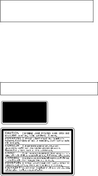
CAUTION
Use of controls or adjustments or performance of procedures other than those specified herein may result in hazardous radiation exposure.
Notes on chip component replacement
•Never reuse a disconnected chip component.
•Notice that the minus side of a tantalum capacitor may be damaged by heat.
Flexible Circuit Board Repairing
•Keep the temperature of soldering iron around 270˚C during repairing.
•Do not touch the soldering iron on the same conductor of the circuit board (within 3 times).
•Be careful not to apply force on the conductor when soldering or unsoldering.
Laser component in this product is capable of emitting radiation exceeding the limit for Class 1.
This appliance is classified as a CLASS 1 LASER product. The CLASS 1 LASER PRODUCT MARKING is located on the rear exterior.
This caution label is located inside the unit.
SAFETY-RELATED COMPONENT WARNING !!
COMPONENTS IDENTIFIED BY MARK 0OR DOTTED LINE WITH MARK 0 ON THE SCHEMATIC DIAGRAMS AND IN
THE PARTS LIST ARE CRITICAL TO SAFE OPERATION. REPLACE THESE COMPONENTS WITH SONY PARTS WHOSE PART NUMBERS APPEAR AS SHOWN IN THIS MANUAL OR IN SUPPLEMENTS PUBLISHED BY SONY.
2
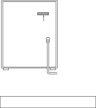
MODEL IDENTIFICATION
— BACK PANEL —
Parts No.
MODEL |
PARTS No. |
|
MY, SP model |
4-227-751-2s |
|
EA model |
4-227-751-3s |
|
• Abbreviation |
|
|
SP |
: Singapore model |
|
EA |
: Saudi Arabia model |
|
MY |
: Malaysia model |
|
NOTES ON HANDLING THE OPTICAL PICK-UP BLOCK OR BASE UNIT
The laser diode in the optical pick-up block may suffer electrostatic break-down because of the potential difference generated by the charged electrostatic load, etc. on clothing and the human body.
During repair, pay attention to electrostatic break-down and also use the procedure in the printed matter which is included in the repair parts.
The flexible board is easily damaged and should be handled with care.
NOTES ON LASER DIODE EMISSION CHECK
The laser beam on this model is concentrated so as to be focused on the disc reflective surface by the objective lens in the optical pickup block. Therefore, when checking the laser diode emission, observe from more than 30 cm away from the objective lens.
LASER DIODE AND FOCUS SEARCH OPERATION CHECK
Carry out the “S curve check” in “CD section adjustment” and check that the S curve waveform is output four times.
3
TABLE OF CONTENTS
1. SERVICING NOTE .......................................................... |
5 |
2. GENERAL .................................................................... |
9 |
3. DISASSEMBLY |
|
3-1. Front Panel and Video Board .............................................. |
11 |
3-2. Main Board ......................................................................... |
11 |
3-3. Sub Panel ............................................................................ |
12 |
3-4. CD LID Assembly .............................................................. |
12 |
3-5. Tape Mechanism Deck and Cassette LID ........................... |
12 |
3-6. CD Mechanism Deck .......................................................... |
13 |
3-7. Base Unit ............................................................................. |
13 |
3-8. Disc Table ........................................................................... |
13 |
4. TEST MODE .............................................................. |
14 |
5. MECHANICAL ADJUSTMENTS .......................... |
15 |
6. ELECTRICAL ADJUSTMENTS ............................... |
15 |
7. DIAGRAMS |
|
7-1. Circuit Boards Location ...................................................... |
19 |
7-2. Block Diagrams |
|
• BD Section ....................................................................... |
20 |
• Deck Section .................................................................... |
21 |
• Main (1/2) Section ........................................................... |
22 |
• Main (2/2) Section ........................................................... |
23 |
• Video Section ................................................................... |
24 |
• Power Section .................................................................. |
25 |
• Display Section ................................................................ |
26 |
7-3. Printed Wiring Board – BD Section – ................................. |
28 |
7-4. Schematic Diagram – BD Section – ................................... |
29 |
7-5. Schematic Diagram – Deck Section – ................................. |
30 |
7-6. Printed Wiring Board – Deck Section – .............................. |
31 |
7-7. Printed Wiring Board – Video Section – ............................. |
32 |
7-8. Schematic Diagram – Video (1/3) Section – ....................... |
33 |
7-9. Schematic Diagram – Video (2/3) Section – ....................... |
34 |
7-10. Schematic Diagram – Video (3/3) Section – ..................... |
35 |
7-11. Printed Wiring Board – Main Section – ............................ |
36 |
7-12. Schematic Diagram – Main (1/3) Section – ...................... |
37 |
7-13. Schematic Diagram – Main (2/3) Section – ...................... |
38 |
7-14. Schematic Diagram – Main (3/3) Section – ...................... |
39 |
7-15. Printed Wiring Board – Power Section – ......................... |
40 |
7-16. Schematic Diagram – Power Section – ............................ |
41 |
7-17. Printed Wiring Board – Panel FL Section – ..................... |
42 |
7-18. Schematic Diagram – Panel FL Section – ........................ |
43 |
7-19. Printed Wiring Board – Panel VR Section – .................... |
44 |
7-20. Schematic Diagram – Panel VR Section – ....................... |
45 |
7-21. Printed Wiring Board – TC Panel Section – ..................... |
46 |
7-22. Schematic Diagram – TC Panel Section – ....................... |
47 |
7-23. Printed Wiring Board – CD Panel Section – .................... |
48 |
7-24. Schematic Diagram – CD Panel Section – ....................... |
49 |
7-25. Printed Wiring Board – CD Motor Section – ................... |
50 |
7-26. Schematic Diagram – CD Motor Section – ...................... |
51 |
7-27. Schematic Diagram – Trans Section – ............................. |
52 |
7-28. Printed Wiring Board – Trans Section – ........................... |
53 |
7-29. Schematic Diagram – Leaf SW Section – ........................ |
53 |
7-30. Printed Wiring Board – Leaf SW Section – ..................... |
53 |
7-31. IC Block Diagrams ........................................................... |
54 |
7-32. IC Pin Functions ............................................................... |
56 |
8. EXPLODED VIEWS
8-1. Case and Back Panel Section .............................................. |
66 |
|
8-2. Front Panel Section 1 .......................................................... |
67 |
|
8-3. Front Panel Section 2 .......................................................... |
68 |
|
8-4. Chassis Section ................................................................... |
69 |
|
8-5. |
TC Mechanism Section 1 (TCM230PWR12) ..................... |
70 |
8-6. |
TC Mechanism Section 2 (TCM230PWR12) ..................... |
71 |
8-7. |
CD Mechanism Section (CDM37L-5BD34L) .................... |
72 |
8-8. |
Base Unit Section (BU-5BD34L) ....................................... |
73 |
9. ELECTRICAL PARTS LIST ........................................ |
74 |
|
4
SECTION 1
SERVICING NOTE
About CD-TEXT display
This unit is provided with a simple CD-TEXT display function.
The CD-TEXT contents of 20 tracks are displayed on the fluorescent display tube.
Since the function is simple, some special characters may not be displayed, or may be displayed as other characters.
MC Cold Reset
• The cold reset clears all data including preset data stored in the RAM to initial conditions. Execute this mode when returning the set to the customer.
Procedure:
1. Press three buttons c/CLOCK SET , ENTER , and "/1 simultaneously.
2. “COLD RESET” is displayed on the fluorescent display tube and reset is executed.
CD Delivery Mode
• This mode moves the pick-up to the position durable to vibration. Use this mode when returning the set to the customer after repair.
Procedure:
1. |
Press |
"/1 |
button to turn the set ON. |
||||
2. |
Press |
|
|
|
button and |
"/1 |
button simultaneously. |
|
LOOP |
||||||
3. |
A message “LOCK” is displayed on the fluorescent indicator tube, and the CD delivery mode is set. |
||||||
MC Hot Reset
•This mode resets the set with the preset data kept stored in the memory. The hot reset mode functions same as if the power cord is plugged in and out.
Procedure:
1. |
Press three buttons |
c/CLOCK SET |
, |
ENTER |
, and |
DISC 1 |
simultaneously. |
2. |
The fluorescent indicator tube becomes blank instantaneously, and the set is reset. |
||||||
Sled Servo Mode
• This mode can run the CD sled motor freely. Use this mode, for instance, when cleaning the pick-up.
Procedure:
1.Press "/1 button to turn the set ON.
2.Press three buttons c/CLOCK SET , ENTER , and DISC 5 simultaneously.
3.The Sled Servo mode is selected, if “CD” is blanking on the fluorescent indicator tube.
4.With the CD in stop status, When the M button is pressed, the optical pick-up moves outside. When m button is pressed, it moves inside.
5.To exit from this mode, perform as follows:
1)Move the pick-up to the most inside track.
2)Execute MC cold reset. (Press the three buttons c/CLOCK SET , ENTER , and "/1 button simultaneously.)
Note:
•Always move the pick-up to most inside track when exiting from this mode. Otherwise, a disc will not be unloaded.
•Do not run the sled motor excessively, otherwise the gear can be chipped.
Change-over of AM Tuner Step between 9kHz and 10kHz
• A step of AM channels can be changed over between 9kHz and 10kHz.
Procedure:
1.Press "/1 button to turn the set ON.
2.Select the function “TUNER”, and press TUNER/BAND button to select the BAND “AM”.
3.Press "/1 button to turn the set OFF.
4.Press ENTER and "/1 buttons simultaneously, and the display of fluorescent indicator tube changes to “AM 9k STEP” or “AM 10k STEP”, and thus the channel step is changed over.
LED and Fluorescent Indicator Tube All Lit, Key Check Mode
Procedure:
1. Press three buttons c/CLOCK SET , ENTER , and DISC 2 simultaneously.
2.LEDs and fluorescent indicator tube are all turned on. Press DISC 2 button, and the key check mode is activated.
3.In the key check mode, the fluorescent indicator tube displays “K @ V0 J0”. Each time a button is pressed, “K”value increases. However, once a button is pressed, it is no longer taken into account.
“J” Value increases like 1, 2, 3 ... if rotating .AMS > knob in “+” direction, or it decreases like 0, 9, 8 ... if rotating in “-” direction.
“V” Value increases like 1, 2, 3 ... if rotating VOLUME knob in “+” direction, or it decreases like 0, 9, 8 ... if rotating in “-” direction.
4.To exit from this mode, press three buttons in the same manner as step 1, or disconnect the power cord.
5
AMS Test Mode
• This mode is used for checking the AMS operations of the tape deck.
JIG
7-819-039-12 Alignment tape, AMS-110A
Procedure:
1.Press the "/1 button to turn the set ON.
2.Set the tape (AMS-110A).
3.Press the three buttons c/CLOCK SET , ENTER , and DISC 3 button simultaneously.
4.“TEST MODE” is displayed on the fluorescent display tube.
5.Press the FUNCTION button and switch the function to the deck with the tape (AMS-110A).
6.Press the CD SYNC button. “AMS CHECK” is displayed on the fluorescent display tube and the tape is rewound.
7.AMS starts in the normal direction. If the AMS count is 2 at shut down, proceed to step 8. “NG” is displayed at other times, and the deck stops.
8.AMS starts in the opposite direction. If the AMS count is 2 at shut down again, “OK” is displayed. “NG” is displayed at other times.
Aging Mode
During the aging mode, both the CD player and tape deck are executed together.
• If an error occurs:
Aging stops, and the error state is displayed on the fluorescent display tube.
• If no error occurs:
Aging is repeated.
Procedure:
1.Press the "/1 button to turn the set ON.
2.Load 10 minute tapes with unbent rec-proof tabs in decks A and B.
3.Set CDs on the DISC 1 and DISC 4 tables.
4.Set the CD mode REPEAT to OFF and PLAY MODE to ALL DISCS.
|
(Press the |
PLAY MODE |
and |
REPEAT |
buttons to set these modes.) |
|||||||||
5. |
Press the |
|
|
|
|
button to switch the function to “CD”. |
||||||||
FUNCTION |
|
|||||||||||||
6. |
Press the three buttons |
|
|
|
|
|
, |
|
, and |
|
button simultaneously. |
|||
|
c/CLOCK SET |
ENTER |
DISC 4 |
|||||||||||
7.Aging starts.
8.To end aging, press the "/1 button to turn the set OFF.
Aging Sequence:
Aging is performed in the following sequence.
• Tape Deck
1.The tape in deck A is rewound. “TAPE A AG-1” is displayed.
2.The FWD side of deck A is played for two minutes. “TAPE A AG-2” is displayed.
3.The tape in deck A is fast forwarded. “TAPE A AG-3” is displayed. Fast forward is carried out for 20 seconds or to the tape end.
4.The RVS side of deck A is played for two minutes. “TAPE A AG-4” is displayed.
5.The tape in deck A is rewound. “TAPE A AG-5” is displayed.
6.The FWD side of deck B is played for two minutes. “TAPE B AG-2” is displayed.
7.The tape in deck B is fast forwarded. “TAPE B AG-3” is displayed. Fast forward is carried out for 20 seconds or to the tape end.
8.The RVS side of deck B is played for two minutes. “TAPE B AG-4” is displayed.
9.The tape in deck A is rewound. “TAPE A AG-5” is displayed.
10.Repeated from step 2.
6
• CD
1.The tray rotates.
2.DISC 1 is chucked.
3.The TOC is read.
4.The first track is played for 2 seconds.
5.The last track is played for 2 seconds.
6.The tray rotates.
7.DISC 4 is chucked.
8.The TOC is read.
9.The first track is played for 2 seconds.
10.The last track is played for 2 seconds.
11.Repeated from step 1.
• Display when ended abnormally When the tape deck is abnormal:
The state when ended abnormally is displayed.
The contents of display are the same as that during aging.
When the CD player is abnormal:
A message indicating that errors such as “CD MEC ERR” have occurred.
Check the error contents in the following error history display mode.
Error History Display Mode
Mode which enables the history of error occurring in the CD player to be checked.
Execute this mode after ending the aging mode.
Procedure:
1. Press the "/1 button to turn the set ON.
2. Press the three buttons c/CLOCK SET , ENTER , and CD SYNC simultaneously.
3.A message such as “EMC@@EDC**” is displayed.
@@ : Number of mechanical errors (Up to three past errors)
**: Number of errors (NO DISC ERROR) which occurs after chucking (Up to three past errors)
4.When checking the history of mechanical errors, press the PLAY MODE button. When checking errors after chucking, press the REPEAT button to switch the display.
5.Press the "/1 button to end and turn the set OFF.
6.To erase the error history, perform COLD reset.
(Press the three buttons c/CLOCK SET , ENTER , and DISC 1 simultaneously.
•Viewing the mechanical error history display
(Switch the history by pressing the PLAY MODE button.)
7
Display
E@@M#*****
@@ : Error number. 00 is the newest.
#: Operating state of table
0 : Currently in the INITIAL mode
7: Currently rotating to the right
8: Currently rotating to the left A : Currently chucking down B : Currently chucking up
*: Invalid
•Viewing the NO DISC ERROR history display (Switch the history by pressing the REPEAT button.)
Display
E@@D##$$%*
@@ : Error number. 00 is the newest
##: Error contents
01:Focus error
02:GFS error
03:Setup error
$$ : Retries
00: NO DISC is determined without attempting chucking retry
02:NO DISC is determined after chucking retry.
%: State when determined as NO DISC
1: When stopped
2: At setup
3: At TOC READ
4: When accessing
5: When playing
6: When pausing
7: When manual searching (during play)
8: When manual searching (during pausing) * : Invalid
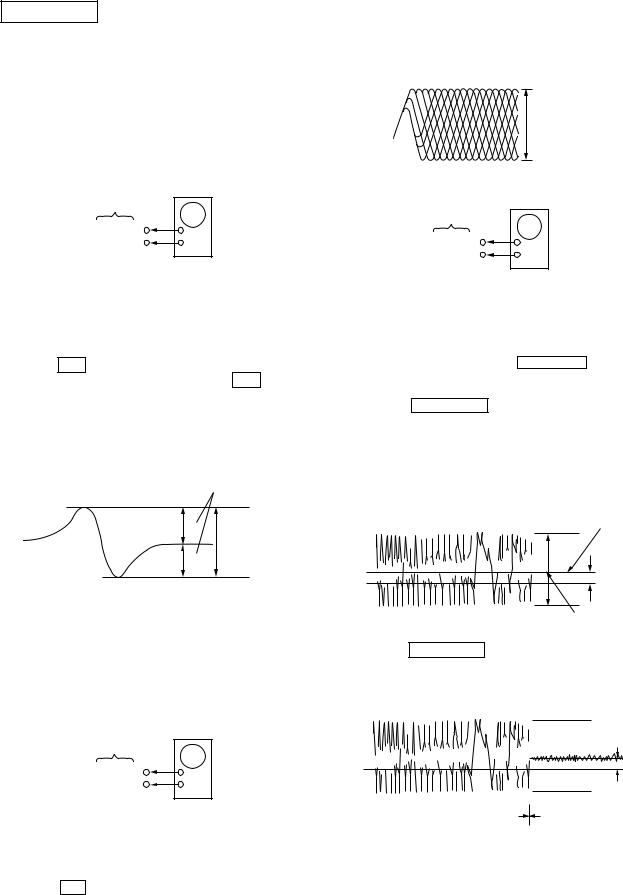
SELF-DIAGNOSIS
This model has the self-diagnosis function for the VIDEO and AUDIO decoder sections.
Immediately after the power on, the self-diagnosis function searches each operation of IC’s around the mechanism control microcomputer (IC701).
The results can be checked by D502 of the VIDEO board.
|
|
Oscilloscope (Waveform) |
Symptom |
[VIDEO BOARD] (SIDE A) |
|
|||||||||||||||
|
|
|
|
|||||||||||||||||
|
|
|
|
|
|
|
|
|
|
|
|
|
|
|
|
|
|
|
|
|
|
|
|
|
|
|
|
|
|
|
|
|
|
|
|
H |
|
D502 |
|
||
|
|
|
|
|
|
|
|
|
|
|
|
|
|
|
|
|||||
|
|
|
|
|
|
|
|
|
|
|
|
|
|
|
|
|
|
|
|
|
|
|
|
|
|
|
|
|
|
|
|
|
|
|
|
L |
No error |
|
|
||
|
|
|
|
|
|
|
|
|
|
|
|
|
|
|
|
|
|
|||
|
|
|
|
|
|
Light |
|
100 |
91 |
|||||||||||
|
|
|
|
|
|
|
|
|
|
|
|
|
|
|
|
|
|
|
||
|
|
|
|
|
|
|
|
|
|
|
|
|
|
|
|
|
|
|
1 |
90 |
|
|
|
|
|
|
|
|
|
|
|
|
|
|
|
H |
MPEG decoder (IC505) |
IC505 |
|
||
|
|
|
|
|
|
|
|
|
|
|
|
|
|
|
|
|
|
|
||
|
|
|
|
|
|
|
|
|
|
|
|
|
|
|
|
|
|
32 |
65 |
|
|
|
|
|
|
|
|
|
|
|
|
|
|
|
|
L |
error |
||||
|
|
|
|
|
|
|
|
|
|
|
|
|
|
|
33 |
64 |
||||
|
|
|
|
|
2 time blinking |
|
||||||||||||||
|
|
|
|
|
|
|
|
|||||||||||||
|
|
|
|
|
|
|
|
|
|
|
|
|
|
|
|
|
|
|
|
|
|
|
|
|
|
|
|
|
|
|
|
|
|
|
|
|
|
H |
MPEG decoder (IC505) |
|
|
|
|
|
|
|
|
|
|
|
|
|
|
|
|
|
|
|
|
|
||
|
|
|
|
|
|
|
|
|
|
|
|
|
|
|
|
|
|
|
|
|
|
|
|
|
|
|
|
|
|
|
|
|
|
|
|
|
|
L |
or |
|
|
|
|
|
|
|
|
|
|
|
|
|
|
|
|
|
|
|
|
|
||
|
|
|
|
|
|
3 time blinking |
DRAM (IC507) error |
|
|
|||||||||||
|
|
|
|
|
|
|
|
|
|
|
|
|
|
|
|
|
|
|
|
|
8
SECTION 2
GENERAL
Front Panel
|
|
|
|
1 |
2 |
3 |
4 |
5 |
6 |
|
7 |
8 |
9 |
10 |
11 12 |
13 |
14 |
|
|
|
|
|
|
|
|
|
|
|
|
|
|
|
|
|
|
|
|
|
||||
|
|
|
|
|
|
|
|
|
|
|
|
|
|
|
|
|
|
|
|
|
|
|
|
|
|
|
|
|
|
|
|
|
|
|
15 |
|
|
|
|
|||
|
|
|
|
|
|
|
|
|
|
|
|
|
|
|
|
|
|
|
|
|
|
|
|
|
|
|
|
|
|
|
|
|
|
|
16 |
|
|
|
|
|||
|
|
|
|
|
|
|
|
|
|
|
|
|
|
|
|
|
|
|
|
|
|
|
|
|
|
|
|
|
|
|
|
|
|
|
17 |
|
|
|
|
|||
|
|
|
73 |
|
|
|
|
|
|
|
|
|
|
|
|
|
|
|
|
|
|
|
|
|
|
|
|
|
|
|
|
|
|
|
74 |
|
|
|
|
|||
|
|
|
|
|
|
|
|
|
|
|
|
|
|
|
|
|
|
|
|
|
|
|
|
|
|
|
|
|
|
|
|
|
|
18 |
|
|
|
|
||||
|
|
|
|
|
|
|
|
|
|
|
|
|
|
|
|
|
|
|
|
|
|
|
|
|
|
|
|
|
|
|
|
|
|
|
|
|
|
|
||||
|
|
|
72 |
|
|
|
|
|
|
|
|
|
|
|
|
|
|
|
|
|
|
|
|
|
|
|
|
|
|
|
|
|
|
|
75 |
|
|
|
|
|||
|
|
|
71 |
|
|
|
|
|
|
|
|
|
|
|
|
|
|
|
|
|
|
|
|
|
|
|
|
|
|
|
|
|
|
|
19 |
|
|
|
|
|||
|
|
|
70 |
|
|
|
|
|
|
|
|
|
|
|
|
|
|
|
|
|
|
|
|
|
|
|
|
|
|
|
|
|
|
|
|
|
|
|
|
|
|
|
|
|
|
69 |
|
|
|
|
|
|
|
|
|
|
|
|
|
|
|
|
|
|
|
|
|
|
|
|
|
|
|
|
|
|
|
|
|
|
|
|
|
|
|
|
|
|
68 |
|
|
|
|
|
|
|
|
|
|
|
|
|
|
|
|
|
|
|
|
|
|
|
|
|
|
|
|
|
|
|
20 |
|
|
|
|
|||
|
|
|
|
|
|
|
|
|
|
|
|
|
|
|
|
|
|
|
|
|
|
|
|
|
|
|
|
|
|
|
|
|
|
|
|
|
|
|
|
|
|
|
|
|
|
67 |
|
|
|
|
|
|
|
|
|
|
|
|
|
|
|
|
|
|
|
|
|
|
|
|
|
|
|
|
|
|
|
|
|
|
|
|
|
|
|
64 |
65 |
66 |
|
|
|
|
|
|
|
|
|
|
|
|
|
|
|
|
|
|
|
|
|
|
|
|
|
|
|
|
|
|
|
|
|
|
|
|
|
|
||
|
|
|
63 |
|
|
|
|
|
|
|
|
|
|
|
|
|
|
|
|
|
|
|
|
|
|
|
|
|
|
|
|
|
|
|
|
|
|
|
|
|
|
|
|
|
|
|
|
|
|
|
|
|
|
|
|
|
|
|
|
|
|
|
|
|
|
|
|
|
|
|
|
|
|
|
|
|
|
|
|
|
|
|
|
|
|
|
|
|
|
|
|
|
|
|
|
|
|
|
|
|
|
|
|
|
|
|
|
|
|
|
|
|
|
|
|
|
|
|
|
|
|
|
|
|
|
|
|
|
60 |
61 62 |
|
|
|
|
|
|
|
|
|
|
|
|
|
|
|
|
|
|
|
|
|
|
|
|
|
|
|
|
|
|
|
|
|
|
|
|
|
|
|
||
|
|
|
|
|
|
|
|
|
|
|
|
|
|
|
|
|
21 |
22 |
|
|
|
|||||||||||||||||||||
58 |
|
59 |
|
|
|
|
|
|
|
|
|
|
|
|
|
|
|
|
|
|
|
|
||||||||||||||||||||
|
|
|
|
|
|
|
|
|
|
|
|
|
|
|
|
|
|
|
|
|
|
|
|
|
|
|
|
|
|
|
|
23 |
|
|
|
|
||||||
|
|
|
|
|
|
|
|
|
|
|
|
|
|
|
|
|
|
|
|
|
|
|
|
|
|
|
|
|
|
|
|
|
|
|
||||||||
|
|
|
|
|
|
|
|
|
|
|
|
|
|
|
|
|
|
|
|
|
|
|
|
|
|
|
|
|
|
|
|
|
|
|
|
|
|
|
|
|
|
|
|
|
|
|
|
|
|
|
|
|
|
|
|
|
|
|
|
|
|
|
|
|
|
|
|
|
|
|
|
|
|
|
|
|
|
|
|
|
|
|
|
|
|
|
|
|
|
|
|
|
|
|
|
|
|
|
|
|
|
|
|
|
|
|
|
|
|
|
|
|
|
|
|
|
|
|
|
|
|
|
|
|
|
|
|
|
|
56 |
57 |
|
|
|
|
|
|
|
|
|
|
|
|
|
|
|
|
|
|
|
|
|
|
|
|
|
|
|
|
|
|
24 |
|
|
25 |
|
|
||||
|
|
|
|
|
|
|
|
|
|
|
|
|
|
|
|
|
|
|
|
|
|
|
|
|
|
|
|
|
|
|
|
|
|
|
||||||||
|
|
|
|
|
|
|
|
|
|
|
|
|
|
|
|
|
|
|
|
|
|
|
|
|
|
|
|
|
|
|
|
|
|
|
|
|
|
|
||||
53 |
54 |
55 |
|
|
|
|
|
|
|
|
|
|
|
|
|
|
|
|
|
|
|
|
|
|
|
|
|
|
|
26 |
27 |
|
28 |
|||||||||
|
|
|
|
|
|
|
|
|
|
|
|
|
|
|
|
|
|
|
|
|
|
|
|
|
|
|
|
|
||||||||||||||
|
|
|
|
|
|
|
|
|
|
|
|
|
|
|
|
|
|
|
|
|
|
|
|
|
|
|
|
|
|
|
29 |
|
|
30 |
|
|
||||||
51 |
52 |
|
|
|
|
|
|
|
|
|
|
|
|
|
|
|
|
|
|
|
|
|
|
|
|
|
|
|
|
|
|
|
|
|
|
|
|
|
|
|
||
|
|
|
|
|
|
|
|
|
|
|
|
|
|
|
|
|
|
|
|
|
|
|
|
|
|
|
31 |
32 |
|
|
|
|
||||||||||
|
|
|
|
|
|
|
|
|
|
|
|
|
|
|
|
|
|
|
|
|
|
|
|
|
|
|
|
|
|
|
|
|
|
|||||||||
|
|
|
|
|
|
|
|
|
|
|
|
|
|
|
|
|
|
|
|
|
|
|
|
|
|
|
|
|
|
|
|
|
|
|
||||||||
|
|
|
|
|
|
|
|
|
|
|
|
|
|
|
|
|
|
|
|
|
|
|
|
|
|
|
|
|
|
|
|
|
|
|
|
|
|
|
|
|
|
|
|
|
|
|
|
|
|
|
|
|
|
|
|
|
|
|
|
|
|
|
|
|
|
|
|
|
|
|
|
|
|
|
|
|
|
33 |
|
|
|
|
|||
|
|
|
50 |
|
|
|
|
|
|
|
|
|
|
|
|
|
|
|
|
|
|
|
|
|
|
|
|
|
|
|
|
|
|
|
34 |
|
|
|
|
|||
|
|
|
|
|
|
|
|
|
|
|
|
|
|
|
|
|
|
|
|
|
|
|
|
|
|
|
|
|
|
|
|
|
|
|
|
|
|
|||||
|
|
|
|
|
|
|
|
|
|
|
|
|
|
|
|
|
|
|
|
|
|
|
|
|
|
|
|
|
|
|
|
|
|
|
|
|
|
|||||
|
|
|
|
|
|
|
|
|
|
|
|
|
|
|
|
|
|
|
|
|
|
|
|
|
|
|
|
|
|
|
|
|
|
|
|
|
|
|||||
|
|
|
|
|
|
|
|
|
|
|
|
|
|
|
|
|
|
|
|
|
|
|
|
|
|
|
|
|
|
|
|
|
|
|
|
|
|
|
|
|
|
|
|
|
|
|
|
|
|
|
|
|
|
|
|
|
|
|
|
|
|
|
|
|
|
|
|
|
|
|
|
|
|
|
|
|
|
|
|
|
|
|
|
|
|
|
|
|
49 |
|
|
|
|
|
|
|
|
|
|
|
|
|
|
|
|
|
|
|
|
|
35 |
36 |
|
37 |
||||||||||||||
|
|
|
48 |
|
|
|
|
|
|
|
|
|
|
|
|
|
|
|
|
|
|
|
|
|
|
|
|
|
|
|
|
|
|
|
38 |
|
|
|
|
|||
|
|
|
47 |
|
|
|
|
|
|
|
|
|
|
|
|
|
|
|
|
|
|
|
|
|
|
|
|
|
|
|
|
|
|
|
|
|
|
|
||||
|
|
|
|
|
|
|
|
|
|
|
|
|
|
|
|
|
|
|
|
|
|
|
|
|
|
|
|
|
|
|
|
|
|
|
|
|
|
|
|
|
|
|
|
|
|
|
|
|
|
|
|
|
|
|
|
|
|
|
|
|
|
|
|
|
|
|
|
|
|
|
|
|
|
|
|
|
|
39 |
|
|
|
|
|||
|
|
|
|
|
|
|
|
|
46 |
45 |
44 |
43 |
42 |
|
|
|
80 79 |
41 40 |
76 |
|
|
|
|
|
|
|
|
|
|
|
|
|
|
|
|
|
|
|||||
|
|
|
|
|
|
|
|
|
|
|
|
|
|
|
|
|
|
|
|
|
|
|
|
|
|
|
|
|
|
|||||||||||||
|
|
|
|
|
|
|
|
|
|
|
|
|
|
|
|
|
|
|
|
|
77 |
|
|
|
|
|
|
|
|
|
|
|
|
|
|
|
|
|
|
|||
|
|
|
|
|
|
|
|
|
|
|
|
|
|
|
|
|
|
|
|
|
|
|
|
|
|
|
|
|
|
|
|
|
|
|
|
|
|
|
||||
|
|
|
|
|
|
|
|
|
|
|
|
|
|
|
|
|
|
|
|
|
78 |
|
|
|
|
|
|
|
|
|
|
|
|
|
|
|
|
|
|
|||
|
|
|
|
|
|
|
|
|
|
|
|
|
|
|
|
|
|
|
|
|
|
|
|
|
|
|
|
|
|
|
|
|
|
|
|
|
|
|
||||
9
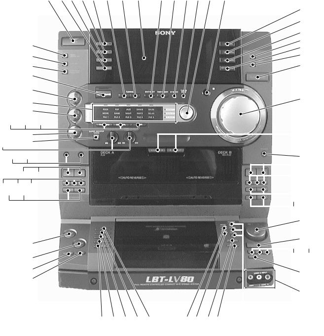
LOCATION OF PARTS AND CONTROLS
1 |
"/1(Power) button and indicator |
28 |
M(B Deck) button |
55 |
M(A Deck) button |
2 |
c/CLOCK SET button |
29 |
X(B Deck) button and indicator |
56 |
h(A Deck) button |
3 |
SLEEP button |
30 |
zREC (B Deck) button and indicator |
57 |
H(A Deck) button |
4 |
REC button and indicator |
31 |
H SPEED DUB button |
58 |
MIX MIC jack |
5 |
DAILY button and indicator |
32 |
CD SYNC button |
59 |
GUITAR jack |
6 |
TUNING - button |
33 |
.AMS >knob |
60 |
MIC LEVEL knob |
7 |
TUNING + button |
34 |
HX(CD) button and indicator |
61 |
GUITAR LEVEL knob |
8 |
Display window |
35 |
x(CD) button |
62 |
SUPER WOOFER MODE button |
9 |
ENTER/NEXT button and indicator |
36 |
m(CD) button |
63 |
SUPER WOOFER button and indicator |
10 |
TUNER MEMORY button |
37 |
M(CD) button |
64 |
FILE MENU button |
11 |
STEREO/MONO button |
38 |
DISK SKIP button |
65 |
GEQ CTRL button |
12 |
TUNING MODE button |
39 |
VIDEO2 INPUT jacks |
66 |
ENTER button and indicator |
13 |
GEQ control button |
40 |
REPEAT button |
67 |
GROOVE button and indicator |
14 |
Remote sensor |
41 |
PLAY MODE button |
68 |
Equalizer indicators |
15 |
SYNC EQ button |
42 |
DISC 1 button |
69 |
EFFECT button and indicator |
16 |
SYNC BASS button |
43 |
DISC 2 button |
70 |
TUNER/BAND button |
17 |
SURROUND button and indicator |
44 |
DISC 3 button |
71 |
SPECTRUM ANALYZER button |
18 |
KARAOKE PON button |
45 |
DISC 4 button |
72 |
DISPLAY button |
19 |
FUNCTION button |
46 |
DISC 5 button |
73 |
DEMO (STANDBY) button |
20 |
VOLUME knob |
47 |
EDIT button |
74 |
KEY CONTROL # button |
21 |
Z(A Deck) button |
48 |
NON-STOP button and indicator |
75 |
KEY CONTROL 2 button |
22 |
Z(B Deck) button |
49 |
FLASH button |
76 |
RETURN button |
23 |
PHONES jack |
50 |
LOOP button |
77 |
PREV button |
24 |
h(B Deck) button and indicator |
51 |
DIRECTION button |
78 |
NEXT button |
25 |
H(B Deck) button and indicator |
52 |
DOLBY NR button |
79 |
SELECT button |
26 |
x(B Deck) button |
53 |
x(A Deck) button |
80 |
ACTIVE button |
27 |
m(B Deck) button |
54 |
m(A Deck) button |
|
|
• AMS is the abbreviation for Automatic Music Sensor.
This section is extracted from instruction manual.
7
Tip |
If you make a mistake, start over from step 1. |
To change the time |
The previous explanation shows you how to set the time while the power is off. To change the time |
while the power is on, do the following: 1 Press c/CLOCK SET. |
2 Press TUNING +/ – to select SET CLOCK. 3 Press ENTER/NEXT. 4 Perform steps 2 through 5 in the previous explanation. |
Note |
The clock setting is canceled when you disconnect the power cord or if a power failure occurs. |
|
|
|
|
|
|
|
|
Step 2: Setting the |
time |
You must set the time before using the timer |
functions. |
1 2,4 3,5 |
|
1 Press c/CLOCK SET. |
The hour indication flashes. |
2 Press TUNING +/ – to set the hour. |
3 Press ENTER/NEXT. |
The minute indication flashes. |
4 Press TUNING +/ – to set the minute. |
5 Press ENTER/NEXT. |
The clock starts. |
10
SECTION 3
DISASSEMBLY
Note: Follow the disassembly procedure in the numerical order given.
3-1. FRONT PANEL AND VIDEO BOARD
|
9Connector(CN452) |
8Flat type wire(CN303) |
0Connector(CN702) |
|
|
7Flat type wire(CN304) |
|
6Flat type wire |
4Screw(BVTP3x8) |
(CN431) |
|
1Screw(BVTP3x8) |
5Two earth wirs |
2Earth wire |
qf Screw (BVTP 3x8) |
|
wa Bracket (VCD)
w; Connector (CN301)
qdFront panel |
qj Video board |
3Connector (CN802)
|
|
qh Screw |
|
qaScrew(BVTP3x8) |
|
(BVTP 3x8) |
|
qg Screw |
qk Flat type wire |
||
|
(BVTP 3x8) |
||
qsFour screws(BVTP3x8) |
(CN501) |
||
|
|||
|
|
ql Flat type wire (CN503) |
3-2. MAIN BOARD
4Screw(BVTP3x8)
1Two screws(BVTP3x8)
0Back panel
8Three screws(BVTP3x8)
qaTwo screws(BVTP3x8) qsFan motor 

7Two screws(BVTP3x8)
6Two screws(BVTP3x8)
5Seven screws(BVTP3x8)
9Connector(CN903)
3Tuner
2Flat type wire(CN1)
qdTwo screws(BVTP3x8)
qfMain board
11
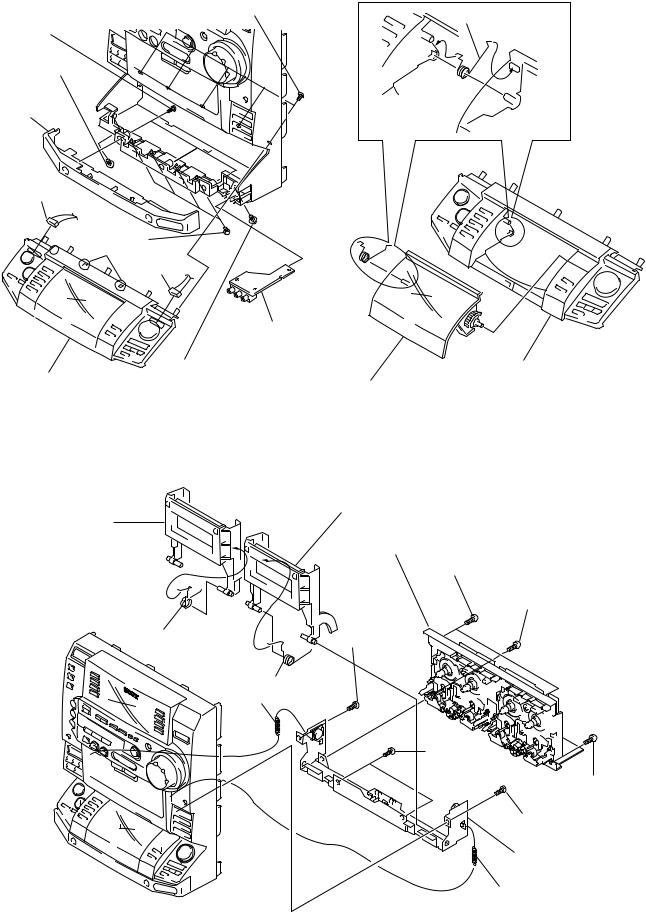
3-3. SUB PANEL |
3-4. CD LID ASSEMBLY |
|
|
5Five screws |
|
1Three screws |
(BVTP2.6x8) |
|
2Spring(CD lid) |
||
(BVTP2.6x8) |
||
|
||
7Screw |
|
|
(BVTP2.6x8) |
|
|
2Ornamental |
|
|
plate |
|
3Connector (CN812)
8Four screws (BVTP2.6x8)
Claw 4Connector  (CN703)
9Front input board
0Sub panel block |
6Screw |
3 Sab panel assembly |
(BVTP2.6x8) |
1CD lid assembly |
|
|
|
3-5. TAPE MECHANISM DECK AND CASSETTE LID
qsHolder(deck B)
qfHolder(deck A)
4Mechanism deck
1Two screws(BVTP3x8)
2Screw(BVTP3x8)
qdSpring(deck A)
7Screw (BVTP3x8)
qaSpring(deck B)
9Spring(TClid)
5Two screws (BVTP3x8)
3Screw(BVTP3x8)
6Screw(BVTP3x8)
0Bracket
8Spring(TClid)
12
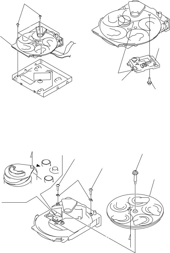
3-6. CD MECHANISM DECK |
3-7. BASE UNIT |
1Five screws (BVTP3x8)
2CD mechanism deck
3Base unit
2Boss
1Yoke fitting
3-8. DISC TABLE
Note:
When the disc table is installed, adjust the positions of roller cam and mark B as shown in the figure, then set to the groove of disc table.
4Stop screw
A |
2Screw (BVTP3X8 |
1Screw (BVTP3X8)
3Bracket (BU) |
5Disc table |
A
13

SECTION 4
TEST MODE
VIDEO CD COLOR-BARS MODE
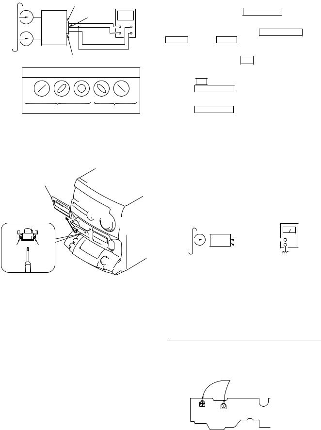
On this mode, the data of the color-bars signal as a picture signal and the 1kHz sine wave signal as a sound signal are output by the mechanism control microcomputer (IC502) for video CD signal check. When measurement of the voltage and waveform on the VIDEO board, perform it in this mode.
For reference, the color-bars signal can be observed at J302 (VIDEO OUT) and the sound signal can be observed at J101 (VIDEO/MD (AUDIO) OUT) using an oscilloscope.
1.Connect the lead wire to both ends of the land of SL503 of the VIDEO board.
2.Turn the power on. Press FUNCTION button to select CD.
3.After 2 or 3 seconds later, connect the lead wire.
4.After measuring, remove the lead wire connected.
[VIDEO BOARD] (SIDE A)
D502
SL501 SL502 SL503
TEST MODE
IC505
CT503 |
|
|
VIDEO |
IC507 |
|
FREQUENCY |
||
|
[VIDEO BOARD] (SIDE B)
TEST |
SL503 |
IC502 |
|
SL502 |
|||
MODE |
|
||
SL501 |
|
||
|
|
14

SECTION 5
MECHANICAL ADJUSTMENTS
Precaution
1.Clean the following parts with a denatured alcohol-moistened swab:
record/playback heads |
pinch rollers |
erase head |
rubber belts |
capstan |
idlers |
2.Demagnetize the record/playback head with a head demagnetizer.
3.Do not use a magnetized screwdriver for the adjustments.
4.After the adjustments, apply suitable locking compound to the parts adjusted.
5.The adjustments should be performed with the rated power supply voltage unless otherwise noted.
Torque Measurement
Mode |
Torque meter |
Meter reading |
|
|
|
3.04 – 6.96 N • m |
|
FWD |
CQ-102C |
(31 to 71 g • cm) |
|
|
|
(0.43 – 0.98 oz • inch) |
|
FWD |
|
0.20 – 0.58 N • m |
|
CQ-102C |
(2 to 6 g • cm) |
||
back tension |
|||
|
(0.02 – 0.08 oz • inch) |
||
|
|
||
|
|
3.04 – 6.96 N • m |
|
REV |
CQ-102RC |
(31 to 71 g • cm) |
|
|
|
(0.43 – 0.98 oz • inch) |
|
REV |
|
0.20 – 0.58 N • m |
|
CQ-102RC |
(2 to 6 g • cm) |
||
back tension |
|||
|
(0.02 – 0.08 oz • inch) |
||
|
|
||
|
|
6.97 – 14.02 N • m |
|
FF/REW |
CQ-201B |
(71 to 143 g • cm) |
|
|
|
(0.98 – 1.99 oz • inch) |
|
|
|
0.98 N • m or more |
|
FWD tension |
CQ-403A |
(100 g or more) |
|
|
|
(3.53 oz or more) |
|
|
|
0.98 N • m or more |
|
REV tension |
CQ-403R |
(100 g or more) |
|
|
|
(3.53 oz or more) |
|
|
|
|
SECTION 6
ELECTRICAL ADJUSTMENTS
DECK SECTION |
|
0 dB=0.775V |
|
|
|
1.Demagnetize the record/playback head with a head demagnetizer.
2.Do not use a magnetized screwdriver for the adjustments.
3.After the adjustments, apply suitable locking compound to the parts adjusted.
4.The adjustments should be performed with the rated power supply voltage unless otherwise noted.
5.The adjustments should be performed in the order given in this service manual. (As a general rule, playback circuit adjustment should be completed before performing recording circuit adjustment.)
6.The adjustments should be performed for both L-CH and R-CH.
7.Switches and controls should be set as follows unless otherwise specified.
Tape |
Signal |
Used for |
|
|
|
P-4-A100 |
10 kHz, –10 dB |
Azimuth Adjustment |
|
|
|
WS-48B |
3 kHz, 0 dB |
Tape Speed Adjustment |
|
|
|
P-4-L300 |
315 Hz, 0 dB |
Level Adjustment |
|
|
|
Record/Playback Head Azimuth Adjustment
(Deck A, Deck B)
Note: Perform this adjustments for both decks.
Procedure:
1. Mode : Playback
test tape |
|
|
|
P-4-A100 |
main board |
|
|
(10kHz, –10dB) |
CN301 |
level meter |
|
|
Pin 1 |
(R-ch) |
|
|
|
||
|
Pin 3 |
(L-ch) |
|
set |
|
|
+ |
|
|
|
– |
2.Turn the adjustment screw and check output peaks. If the peaks do not match for L-CH and R-CH, turn the adjustment screw so that outputs match within 1 dB of peak.
L-CH |
output |
|
|
|
peak |
within |
|
|
|
level |
|
|
||
|
|
|
||
|
|
1 dB |
|
within 1dB |
|
R-CH |
|
|
|
screw |
peak |
|
|
|
|
|
|
|
|
position |
|
|
|
screw |
|
|
L-CH |
R-CH |
|
|
|
position |
||
|
|
peak |
peak |
|
15
3. Mode: Playback
test tape P-4-A100 (10kHz, –10dB)
main board |
|
CN301 |
|
Pin 3 (L-ch) |
oscilloscope |
|
|
Pin 2 (GND) |
|
L |
|
set |
|
R |
|
Pin 1 (R-ch) |
|
Waveform of oscilloscope
in phase |
45° |
90° |
135° |
180° |
|
good |
|
|
wrong |
4.After the adjustments, apply suitable locking compound to the parts adjusted.
Adjustment Location: Playback Head (Deck A)
Record/Playback/Erase Head (Deck B)
Remove the cassette lid.
Reverse Foward
Tape Speed Adjustment (Deck A)
Note: Set the test mode using the following method and begin tape speed adjustment.
In the test mode, the speed will switch to double speed or normal speed each time the HI-SPEED DUB button is pressed.
Procedure:
With the power turned ON, press the c/CLOCK SET button, ENTER button, and DISC 3 button simultaneously.
(The “VOLUME” on the fluorescent display tube will blink while in the test mode.)
To exit the test mode, press the "/1 button.
1.Insert the WS-48B into deck B.
2.Press the H button of deck B.
3.Press the HI-SPEED DUB button and play the tape at double speed.
4.Adjust RV1001 of the LEAF SW board so that the reading of the frequency counter becomes 6000 ± 180 Hz.
5.Press the HI-SPEED DUB button and play the tape at normal speed.
6.Adjust RV1002 of the LEAF SW board so that the reading of the frequency counter becomes 3000 ± 90 Hz.
Adjustment Location: LEAF SW board
Sample Value of Wow and flutter
W.RMS (JIS) less than 0.3% (test tape: WS-48B)
Playback Level Adjustment (Deck A, Deck B)
Procedure:
Mode: Playback
test tape P-4-L300 (315Hz, 0dB)
level meter
set
 main board
CN301
Pin 1 (R-ch)
Pin 3 (L-ch)
Deck A is RV311 (L-CH) and RV411 (R-CH), deck B is RV301 (L-CH) and RV401 (R-CH)
so that adjustment within the following adjustment level.
Adjustment level:
CN301 playback level: 301.5 to 338.3 mV (–8.2 to –7.2 dB) level difference between the channels: within ± 0.5 dB
Adjustment Location: AUDIO board
Adjustment Location
[LEAF SW BOARD]
RV1001(High Speed)
RV1002(Normal Speed)
RV1002 RV1001
16
Record Bias Adjustment (Deck B)
Procedure:
INTRODUCTION
When set to the test mode performed in Tape Speed Adjustment, when the tape is rewound after recording, the “REC memory mode” which rewinds only the recorded portion and playback is set.
This “REC memory mode” is convenient for performing this adjustment. During recording, the input signal FUNCTION will automatically switch to VIDEO 1.
(After recording, press the m button without stopping will return to the position where recording was started.)
1.Press FUNCTION button to select VIDEO 1. (This step is not necessary if the above test mode has already been set.)
2.Insert a tape into deck B, press the z REC button, and then press the H button to start recording.
3.Mode: Record
VIDEO 1 (AUDIO) IN
1)315 Hz } 50 mV (–23.8 dB)
2)10 kHz
AF OSC |
blank tape |
|
|
600 Ω |
CS-123 |
attenuator |
|
|
set |
4. Mode: Playback
recorded |
level meter |
||||
position |
|
|
|
|
|
|
|
|
|
|
|
|
|
|
|
|
|
|
|
|
|
|
|
set
 main board
CN301
Pin 1 (R-ch)
Pin 3 (L-ch)
5.Confirm playback the signal recorded in step 2 become adjustment level as follows.
If these levels do not adjustment level, adjust the RV341 (L-CH) and RV441 (R-CH) on the AUDIO board to repeat steps 3 and 4.
Adjustment level: The playback output of 10 kHz level difference against 315 Hz reference should be ± 1.0 dB.
Adjustment Location: AUDIO board
Record Level Adjustment (Deck B)
Procedure:
INTRODUCTION
When set to the test mode performed in Tape Speed Adjustment, when the tape is rewound after recording, the “REC memory mode” which rewinds only the recorded portion and playback is set.
This “REC memory mode” is convenient for performing this adjustment. During recording, the input signal FUNCTION will automatically switch to VIDEO 1.
(After recording, press the m button without stopping will return to the position where recording was started.)
1.Press FUNCTION button to select VIDEO 1. (This step is not necessary if the above test mode has already been set.)
2.Insert a tape into deck B, press the z REC button, and then press the H button to start recording.
3.Mode: Record
VIDEO 1 (AUDIO) IN 315Hz 50 mV (–23.8 dB)
AF OSC |
blank tape |
|
|
600 Ω |
CS-123 |
attenuator |
|
|
set |
4. Mode: Playback
recorded |
|
level meter |
position |
|
|
|
set |
|
|
main board |
|
|
CN301 |
|
|
Pin 1 |
(R-ch) |
|
Pin 3 |
(L-ch) |
5.Confirm playback the signal recorded in step 2 become adjustment level as follows.
If these levels do not adjustment level, adjust the RV301 (L-CH) and RV351 (R-CH) on the MAIN board to repeat steps 3 and 4.
Adjustment level:
CN301 playback level: 47.2 to 53.0 mV (–24.3 to –23.3 dB)
Adjustment Location: MAIN board
Adjustment Location: |
|
|
[MAIN BOARD] (Conductor Side) |
||
[AUDIO BOARD] (Conductor Side) |
|
|
|
|
|
RV341(Lch),RV441(Rch) |
RV311(Lch),RV411(Rch) |
|
|
|
|
Record Bias |
Playback Level (Deck A) |
|
|
|
|
RV301 RV401 |
|
|
|
|
Record Level (Lch) |
|
|
CN301 |
|
RV301 |
|
|
|
RV411 |
|
||
RV441 RV341 |
RV311 |
|
|
||
3 |
|
|
|||
|
|
|
1 |
|
|
|
|
|
|
43 |
42 |
RV301(Lch),RV401(Rch) |
|
|
IC301 |
56 |
29 |
|
|
1 |
28 |
||
Playback Level (Deck B) |
|
|
|
14 15 |
|
|
|
|
RV351 |
|
|
|
|
|
Record Level (Rch) |
||
17
CD SECTION
Note:
1.CD Block is basically constructed to operate without adjustment. Therefore, check each item in order given.
2.Use YEDS-18 disc (3-702-101-01) unless otherwise indicated.
3.Use an oscilloscope with more than 10MΩ impedance.
4.Clean the object lens by an applicator with neutral detergent when the signal level is low than specified value with the following checks.
S Curve Check
|
oscilloscope |
BD board |
|
TP (FE) |
+ |
TP (VC) |
– |
Adjustment Location: BD board
Procedure :
1.Connect the oscilloscope to test points TP (FE) and TP (VC).
2.Connect TP (FEI) and GND, and TP (AGCCON) and GND of the BD board with lead wires.
3.Press the "/1 button to turn the set ON.
4.With the disc (YEDS-18) loaded, press the 7 button and perform focus search. (Focus search will be performed in the same way even while the disc table is pushed in and out.)
5.Check the symmetry and peak to peak level of the oscilloscope waveform (S curve) at this time.
S-curve waveform
symmetry
A
Within 4.0 ± 1.0 Vp-p
B
6. After check, remove the lead wire connected in step 2.
Note: • Try to measure several times to make sure than the ratio of A : B or B : A is more than 10 : 7.
•Take sweep time as long as possible and light up the brightness to obtain best waveform.
Adjustment Location: BD board
RF Level Check
|
oscilloscope |
BD board |
|
TP (RF) |
+ |
TP (VC) |
– |
Procedure :
1.Connect oscilloscope to test point TP (RF) and TP (VC) on BD board.
2.Connect TP (AGCCON) and GND of the BD board with lead wires.
3.Press the "/1 button to turn the set ON.
4.Put disc (YEDS-18) in and playback 5track.
5.Confirm that oscilloscope waveform is clear and check RF signal level is correct or not.
6.After check, remove the lead wire connected in step 2.
Note: Clear RF signal waveform means that the shape “◊” can be clearly distinguished at the center of the waveform.
RF signal waveform
VOLT/DIV : 200mV
TIME/DIV : 500ns
level : 1.75 ± 0.25 Vp-p
E-F Balance (Traverse) Check
|
oscilloscope |
BD board |
|
TP (TE) |
+ |
TP (VC) |
– |
Adjustment Location: BD board
Procedure :
1.Connect oscilloscpe to test point TP (TE) on BD board.
2.Short-circuit SL502 of the video board to GND.
3.Turned Power switch on. Press FUNCTION button to select CD.
4.Put disc (YEDS-18) in to play the number five track.
5.Press the PLAY MODE button. (The tracking servo and the sledding servo are turned OFF.)
6.Check the level B of the oscilliscope's waveform and the A (DC voltage) of the center of the Traverse waveform.
Confirm the following : A/B x 100 = less than ± 22%
Traverse waveform
|
Center of the waveform |
|
B |
0V |
A (DC voltage) |
|
|
|
level : 1.3 ± 0.6 Vp-p |
7.Press the PLAY MODE button. (The tracking servo and sledding servo are turned ON.) Confirm the C (DC voltage) is almost equal to the A (DC voltage) is step 7.
Traverse waveform
|
C (DC |
0V |
voltage) |
Tracking servo |
Tracking servo |
Sled servo |
Sled servo |
OFF |
ON |
8. Desolder the short-land (SL502) short-circuited at step 2.
Adjustment Location: BD board
18
Adjustment Location :
[ BD BOARD ] — SIDE B —
TP (RF)
TP (VC)
|
TP |
TP |
TP |
(FE) |
(TE) |
|
|
|
(AGCCON) |
|
|
TP |
|
|
(IOP) |
|
|
VIDEO SECTION
Frequency adjustment
1.Connect the frequency counter to check point of the VIDEO board.
2.Adjust CT503 of the VIDEO board so that the frequency counter read 27MHz ± 80Hz at STOP condition.
Adjustment Location :
[ VIDEO BOARD ] – SIDE A –
D502 

SL501 SL502 SL503
TEST MODE
IC505
(27MHz)
CT503
VIDEO IC507
FREQUENCY
(GND)
frequency counter
VIDEO board (27 MHz)
+
–
[ VIDEO BOARD ] – SIDE B –
(27MHz) IC506
(GND)
TEST |
SL503 |
IC502 |
|
SL502 |
|||
|
|||
MODE SL501 |
|
||
7-1. CIRCUIT BOARDS LOCATION
PANEL-FL board
MIC board
TC-A board
PANEL-VR board
TC-B board
LEAF SW board
AUDIO board
CD MOTOR board
HCD-LV80
SECTION 7
DIAGRAMS
TUNER UNIT
VIDEO board
TRANS board |
MAIN board |
|
HEADPHONE board
CD-L board
PA board
CD-R board
FRONT INPUT board
TABLE SENSOR board
BD board
LED board
19 19

HCD-LV80
7-2. BLOCK DIAGRAMS
– BD SECTION –
OPTICAL PICK-UP BLOCK
(KSS-213D/Q-NP)
DETECTOR
E
A
C
A C
D
B D
B
F
E
F
LD
LASER
DIODE
PD
LD
POWER
TRACKING
COIL
FOCUS
COIL
M102
SLED
MOTOR
M101
SPINDLE
MOTOR
|
|
|
|
|
|
|
|
|
|
IC101 |
|
|
|
|
IC103 |
|
|
|
|
|
DIGITAL SERVO |
|
|
|
|
|
|
|
|
|
|
DIGITAL SIGNAL PRCESSOR |
|||
VCC |
|
|
RF AMP |
|
|
|
|
|
|
|
|
VC |
|
A |
|
|
|
|
|
|
|
|
|
|
5 |
|
|
|
|
|
|
|
|
|
|
|
7 |
C |
RF |
|
RFD |
|
|
|
RF AC |
|
|
|
|
D |
SUMMING |
RF EQ |
16 |
|
50 |
|
|
|
|
|
8 |
AMP |
|
|
|
|
|||||
|
AMP |
|
|
|
|
|
|
|
|||
|
6 |
B |
|
|
RFI |
17 |
|
|
|
|
|
|
|
|
|
|
|
|
|
|
|
||
|
|
|
FOCUS |
|
FE |
14 |
INTEG- |
49 |
ASYI |
ASYMMETRY |
|
|
|
|
ERROR |
|
|
||||||
|
|
|
|
|
RATOR |
|
CORRECTION |
||||
|
|
|
AMP |
|
|
|
|
|
|||
|
|
|
|
|
|
|
|
|
|
|
|
|
|
|
|
|
|
|
|
48 |
ASYO |
|
|
|
|
|
|
|
|
|
|
|
|
|
|
|
11 |
E |
TRACKING |
TE |
13 |
|
|
|
|
|
|
|
10 |
F |
ERROR |
|
|
|
|
|
|
|
|
|
AMP |
|
|
|
|
|
|
|
|
||
LD |
3 |
LD |
|
|
|
|
|
|
|
|
|
DRIVE |
|
|
|
|
|
|
|
|
|
|
|
Q101 |
|
|
|
|
|
|
|
|
|
|
|
|
|
|
|
|
VC |
12 |
|
|
|
|
|
|
|
|
|
|
BUFFER |
|
|
|
|
|
|
|
|
|
|
|
|
|
|
|
|
|
|
|
|
|
|
|
|
|
VC |
|
|
|
|
|
|
PD |
APC LD |
|
LD ON |
|
VC |
38 |
|
|
|
|
4 |
|
22 |
|
|
|
|
|
|||
|
|
AMP |
|
|
|
|
|
|
|
||
|
|
|
|
|
|
|
|
RFDC |
|
|
|
|
|
|
|
|
|
|
|
43 |
|
|
|
|
|
|
|
|
REF |
|
|
FE |
|
|
|
|
|
|
|
|
|
|
|
|
|
||
|
|
|
|
|
|
|
|
39 |
|
|
|
|
|
|
|
|
|
|
|
TE |
OP AMP |
A/D |
|
|
|
|
|
|
21 |
|
|
41 |
|||
|
|
|
|
|
|
|
CE |
ANALOG SW |
CONVERTER |
||
|
|
|
|
|
|
|
|
|
|||
|
|
IC102 |
|
|
|
|
VC |
42 |
|
|
|
|
|
|
|
|
|
SE |
|
|
|||
|
FOCUS/TRACKING COIL DRIVE |
|
|
|
INTEG- |
40 |
|
|
|||
|
SPINDLE/SLED MOTOR DRIVE |
|
|
|
RATOR |
|
|
|
|||
|
|
|
|
|
|
|
|
||||
T+ |
12 |
|
|
|
|
|
|
|
|
|
|
|
|
|
|
|
|
|
|
|
|
|
|
T |
|
|
5 |
TFDR |
|
|
|
|
|
PWM |
|
11 |
|
|
|
|
|
|
|
|
|||
|
|
6 |
TRDR |
|
|
|
|
|
GENERATOR |
||
|
|
|
|
|
|
|
|
TFDR |
|
|
|
F+ |
|
|
|
|
|
|
|
31 |
TRACKING |
||
14 |
|
|
|
|
|
|
TRDR |
||||
|
|
|
|
|
|
|
32 |
PWM |
|
||
|
|
|
|
FFDR |
|
|
|
|
GENERATOR |
||
F |
|
|
2 |
|
|
|
|
|
|
|
|
13 |
|
FRDR |
|
|
|
|
FFDR |
|
|
||
|
|
3 |
|
|
|
33 |
FOCUS |
|
|||
|
|
|
|
|
|
|
|
|
|||
SD+ |
|
|
|
|
|
|
|
34 |
FRDR |
PWM |
|
17 |
|
|
|
|
|
|
|
GENERATOR |
|||
|
|
|
|
|
|
|
|
|
|
|
|
M |
|
|
24 |
SFDR |
|
|
|
29 |
SFDR |
SLED |
|
SD |
18 |
|
SRDR |
|
|
|
SRDR |
|
|||
|
|
23 |
|
|
|
30 |
PWM |
|
|||
SP+ |
|
|
|
|
|
|
|
GENERATOR |
|||
15 |
|
|
|
|
|
|
|
|
|
|
|
|
|
|
|
|
|
|
|
|
|
|
|
M |
|
|
25 |
|
|
|
|
25 |
MDP |
|
|
SP |
16 |
|
|
|
|
|
|
|
|
||
|
|
27 |
|
VC |
|
|
|
|
|
|
|
|
|
|
|
|
|
|
|
|
|
||
|
|
|
MUTE 20 |
XRST |
|
|
|
|
|
|
|
|
|
|
|
|
|
|
|
|
|
|
|
EFM
DEMODULATOR
DIGITAL
PLL
DIGITAL
CLV
CONTROL SIGNAL
BLOCK
SERVO
BLOCK
SERVO DSP
TRACKING
SERVO
FOCUS
SERVO
SLED
SERVO
32K RAM
REGISTER
SUB CODE
PROCESSOR
DETECTOR
MIRR
DFCT
FOK
DATA BUS
09
|
|
|
|
|
IC781 |
|
|
|
|
CD DIGITAL |
|
|
|
MD2 |
63 |
D+5V |
OUT |
|
|
|
OPTICAL |
||
ERROR |
DIGITAL |
D OUT |
64 |
1 |
DOUT |
OUT |
|
||||
CORRECTOR |
|
|
|
|
|
|
|
|
|
|
|
|
|
PCM-D |
|
|
ADATA |
|
|
|
66 |
|
|
|
|
BCLK |
67 |
|
BCLK |
D/A |
|
LRCK |
|
||
INTERFACE |
|
65 |
|
LRCK |
|
|
|
|
|||
|
|
C2PO |
|
||
|
|
14 |
|
C2PO |
|
|
|
MUTE |
|
||
|
|
3 |
|
MUTE |
|
|
|
|
|
||
CLOCK |
XTAI |
|
IC104 |
(XTAL 33.8MHz) |
71 |
|
|||
GENERATOR |
|
4 |
MCK |
|
|
|
2 |
||
|
XTSL |
69 |
|
CTRL1 |
|
SENS |
|
||
|
7 |
|
SENS |
|
|
|
|
||
SERVO |
DATA |
4 |
|
DATA |
XLAT |
|
|||
|
|
|
||
AUTO |
5 |
|
XLT |
|
|
|
|||
SEQUENCER |
CLOK |
6 |
|
CLK |
CPU |
SCOR |
|
||
INTERFACE |
15 |
|
SCOR |
|
|
SQSO |
|
||
|
76 |
|
SUBQ |
|
|
SQCK |
|
||
|
77 |
|
SQCK |
|
|
|
|
||
|
S STOP |
26 |
A+5V |
|
|
|
|
||
SERVO |
|
|
S101 |
|
INTERFACE |
SCLK |
|
LIMIT SW |
|
|
8 |
|
SCLK |
|
|
|
|
||
|
|
|
|
LPH |
|
XRST 82 |
|
XRST |
|
|
|
|
|
LD ON |
• SIGNAL PATH
 : CD
: CD
 : VIDEO
 : Digital out
|
DISC |
|
|
TRAY SENS |
|
|
SENSOR |
|
|
||
|
IC202 |
|
|
|
|
S201 |
|
|
|
UP SW |
|
IC201 |
|
|
|||
(UP SWITCH) |
|
|
|||
MOTOR DRIVER |
|
|
|||
|
|
|
|
||
M201 |
3 |
OUT 2 |
IN 2 |
1 |
TBL-R |
TABLE |
M |
|
|
|
|
MOTOR |
7 |
OUT 1 |
IN 1 |
9 |
TBL-L |
|
|||||
+5V |
|
LED SW |
|
LED |
|
|
Q201 |
|
|
||
|
|
|
|
|
|
|
D201 |
|
|
|
|
|
(DISC No.) |
|
|
|
|
A
VIDEO
SECTION
(Page 24)
C
MAIN
SECTION (2/2)
(Page 23)
20 20
HCD-LV80
– DECK SECTION – |
|
|
|
|
|
|
|
|
|
|
|
|
|
|
||
|
|
|
|
|
|
|
|
S1004 |
S1008 |
|
|
|
|
|
PB A/B |
|
|
|
|
|
|
|
|
|
|
|
|
|
|
MS OUT |
|||
|
|
|
|
|
|
|
|
A CrO2 |
B CrO2 |
|
|
|
|
|
||
|
|
|
|
|
|
|
|
|
|
|
|
|
|
CN301 |
|
|
|
|
|
|
RV311 |
|
|
|
|
|
|
|
|
|
3 |
R CH |
|
|
|
|
|
16 |
|
|
17 |
19 |
28 |
27 |
26 |
|
|
|
||
|
|
|
IC611 |
PLAYBACK |
|
|
1 |
|
|
|||||||
|
|
|
PB-A/B |
|
|
A 120/70 B NORM/CROM/ |
|
|
|
|
||||||
|
|
|
LEVEL |
|
|
|
MS |
|
|
|
||||||
|
|
|
|
|
|
|
|
|
|
|||||||
|
L |
|
|
DECK A |
|
|
|
70 |
|
METAL |
|
|
|
|
|
|
|
|
|
|
A IN |
|
|
|
PAS |
|
|
|
|
|
|
||
|
|
|
48 |
|
|
|
|
|
|
PB OUT |
|
|
|
|||
HP101 |
|
|
|
|
|
|
|
|
|
|
40 |
|
TC PB L |
|||
|
|
|
46 |
B IN |
|
|
120 |
|
|
|
|
|
|
|||
PB HEAD |
|
R CH |
|
|
|
|
|
DOL |
|
LM ON/ 25 |
|
|
||||
|
|
|
|
|
|
|
|
|
|
LM ON/OFF |
||||||
(DECK A) |
R |
|
|
|
|
|
|
|
|
|
||||||
|
|
|
|
|
|
|
DOLBY NR |
|
|
OFF |
|
|
|
|||
|
|
|
|
|
|
|
|
DOLBY NR |
|
|
|
|
|
|||
|
|
|
|
|
|
|
|
|
|
|
|
|
|
|||
|
|
|
|
|
|
|
|
|
|
|
|
NORM/ |
|
|
|
|
|
|
|
|
RV301 |
|
|
|
IC301 |
|
|
|
|
|
|
NORM/HIGH |
|
|
|
|
|
|
|
|
|
|
|
|
HIGH |
18 |
|
|||
|
|
|
|
|
|
|
|
|
|
|
|
|
||||
|
|
|
IC601 |
PLAYBACK |
|
|
|
|
|
|
|
|
NR ON/ |
23 |
|
NR ON/OFF |
|
|
|
|
LEVEL |
|
|
|
|
|
|
|
|
OFF |
|
|
|
|
L |
|
|
DECK B |
|
|
|
RV301 |
|
|
|
|
|
24 |
|
REC/PB/PASS |
|
|
|
|
|
|
|
|
|
|
|
PB |
|
||||
REC/PB HEAD |
|
|
|
|
|
|
|
REC LEVEL |
|
|
|
|
|
|
|
|
|
|
|
|
|
|
|
RECOUT |
DOLBY |
|
|
|
|
|
|||
(DECK B) |
|
|
|
|
|
|
|
39 |
|
LIN |
|
|
|
|||
|
R |
R CH |
|
|
|
|
|
|
|
TYPE B |
|
43 |
|
TC REC L |
||
|
|
|
|
36 |
EQOUT |
EQIN |
38 |
|
|
BIAS SW |
|
|
BIAS ON/OFF |
20 |
|
BIAS ON/OFF |
|
|
|
|
|
|
|
|
|
|
|
|
|
RM ON/OFF |
22 |
|
RM ON/OFF |
|
|
3 |
1 |
|
|
|
|
|
D |
M |
|
|
ALC ON/OFF |
15 |
|
ALC ON/OFF |
|
|
|
|
|
|
|
|
|
|
|
|
|
|
|
||
|
|
|
IC602 |
|
|
|
|
|
32 |
31, 33 |
|
|
|
|
|
|
|
|
P |
R |
|
|
|
|
|
|
|
|
|
|
|
|
RELAY |
HRPE101 |
|
|
4 |
|
|
|
|
|
|
|
|
|
|
|
|
|
|
|
REC/PB |
|
|
|
|
|
|
|
|
|
CAP MOTOR |
|
CAPM CNT1 |
||
|
|
|
|
|
|
|
|
|
|
|
|
|
||||
|
|
|
|
RV341 |
|
|
|
|
|
|
|
|
|
CAPM CNT2 |
||
|
|
|
|
|
|
|
|
|
|
|
|
CONTROL |
|
|||
|
|
|
|
REC |
+7.5V |
|
|
|
|
|
|
|
Q336-343 |
|
|
|
|
|
|
|
BIAS |
|
|
|
|
|
|
|
|
|
|
|
|
|
|
|
|
|
Q623 |
|
|
|
|
M1 |
|
SPEED |
SWITCH |
|
||
|
|
|
|
|
|
|
|
|
|
|
|
|||||
|
|
|
|
|
|
|
|
|
|
CAPSTAN |
M |
CONTROL |
CAP M H / L |
|||
|
|
|
|
|
|
|
|
|
|
Q335 |
||||||
|
|
|
|
|
|
|
|
|
|
MOTOR |
|
Q1001 |
B |
|||
|
|
|
|
REC BIAS |
|
|
|
|
|
|
|
|||||
|
|
|
|
|
|
|
|
|
|
|
|
|
|
|
||
|
|
ERASE BIAS |
BIAS OSC |
|
|
|
|
|
|
|
|
|
|
|
||
|
|
T621, Q621, 622 |
|
|
|
|
|
|
|
|
|
|
|
|||
|
|
|
|
|
|
|
|
|
|
|
|
|
|
|
||
ERASE HEAD X |
|
|
|
MAIN (1/2), (2/2) |
RV1002 |
RV1001 |
|
|
SECTION |
|
REEL |
(Page 22, 23) |
||
NORMAL |
HIGH |
|
||
SPEED |
SPEED |
|
DETECT |
A SHUT |
|
IC1001 |
|
||
|
|
|
|
|
|
|
|
REEL |
|
|
|
|
DETECT |
B SHUT |
|
|
|
IC1002 |
|
• R CH : Same as L ch |
|
|
S1001 (A PLAY) |
|
|
+5V |
|
A PLAY |
|
• SIGNAL PATH |
|
|
S1002 (B PLAY) |
B PLAY |
: PB (DECK A) |
|
|
|
|
|
|
|
|
|
: PB (DECK B) |
|
S1003 |
|
A HALF |
: REC (DECK B) |
|
(A HALF) |
+5V |
|
|
|
|
||
|
|
|
+5V |
|
|
|
S1005 |
|
|
|
|
(REC A) |
|
|
09 |
|
S1006 |
|
B HALF/REC A/REC B |
|
|
|
||
|
|
(B HALF) |
|
|
S1009 (REC B)
•PLUNGER SOLENOID is supplied as the MECHANICAL BLOCK ASSY.
A DECK/ |
|
TRIGGER |
|
|
B TRIG |
|
MOTOR |
|
|||
B DECK |
|
|
|
||
|
CONTROL |
|
|
||
PLUNGER |
|
|
A TRIG |
||
|
Q331-334 |
|
|||
|
|
|
|
||
|
|
|
|
|
|
21 21
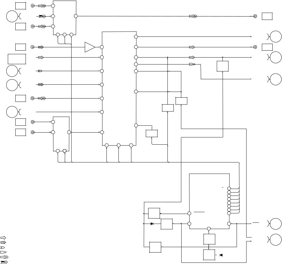
HCD-LV80
– MAIN (1/2) SECTION –
|
|
|
J804 |
|
|
VIDEO 2 |
|
||
|
IN |
|
|
|
VIDEO |
O |
|
|
|
SECTION |
VCD VIDEO |
|||
(Page 24) |
||||
|
J702 |
|||
|
|
|
||
|
VIDEO |
|
|
|
|
IN |
|
|
|
|
|
|
J701 |
|
|
PHONO |
|
|
|
|
(L IN) |
|
|
|
|
FM/AM TUNER |
|
|
|
|
TUNER UNIT IS |
|
ST-L |
|
|
SUPPLED AS THE |
|||
|
ASSEMBLED |
|
|
|
|
BLOCK |
|
|
|
DECK |
B |
|
|
|
SECTION |
|
TC PB L |
||
(Page 21) |
|
|||
|
|
|||
VIDEO |
M |
|
|
|
SECTION |
|
CD-L |
||
(Page 24) |
|
|||
|
|
|||
|
|
|
J701 |
|
|
MD (L IN) |
|
||
POWER |
Q |
|
MIC-SIG |
|
SECTION |
|
|
||
|
|
|
||
(Page 25) |
V1, AU |
|
J701 |
|
|
|
|
||
|
(L IN) |
|
|
|
|
|
|
J804 |
|
|
V2, AU, |
|
|
|
|
L-CH IN |
|
|
|
•R CH: Same as L ch
•SIGNAL PATH
:FM
|
: CD |
|
: PB |
|
: REC |
|
: VIDEO/MD |
09 |
: VIDEO |
IC191
AV SWITCH
6 |
IN3 |
|
8 |
IN4 |
VD OUT 10 |
1 |
IN1 |
IC101 |
|
A |
B |
C |
|
|
SOUND PROCESSOR 1 |
|
||
|
2 |
3 |
5 |
IC601 |
|
|
|
L+R |
30 |
|
46 |
45 |
28 |
|
|
|
|||
|
PHONO AMP |
|
|
|
|
|
|||
|
|
|
|
3 |
1 |
IN A2 |
|
REC B2 |
57 |
|
|
|
|
|
69 |
|
|||
|
|
|
|
|
68 |
IN B2 |
|
BUS OUT2 |
36 |
|
|
|
|
|
|
|
|
REC A2 |
58 |
|
|
|
|
|
67 |
IN C2 |
|
BBA2 |
39 |
|
|
|
|
|
66 |
IN D2 |
|
|
|
|
|
|
|
|
|
|
|
BBB2 |
38 |
|
|
|
|
|
65 |
IN E2 |
|
|
|
IC181 SELECTOR |
|
|
2 |
MIC IN |
|
|
|
||
|
|
|
|
|
|
|
|||
12 |
X0 |
|
|
|
|
|
|
|
|
|
|
|
|
|
|
|
|
BUF IN2 |
37 |
14 |
X1 |
X 13 |
|
|
64 |
IN F2 |
|
|
|
|
|
|
|
|
|
LATCH |
DATA |
CLOCK |
|
|
A |
B |
|
|
|
34 |
33 |
32 |
|
|
|
|
|
|
|
|
|
||
|
10 |
9 |
|
|
|
|
|
|
|
|
46 |
45 |
|
|
|
38 |
47 |
48 |
|
|
|
|
|
|
|
|
|||
J702
VIDEO
OUT
|
SPEANA |
D |
|
|
|
|
J701 |
|
|
|
MD OUT |
|
L-CH SIG |
E |
|
|
|
TC REC L |
MUTE |
|
|
|
|
|
SWITCH |
|
|
Q113 |
|
|
TC REC L |
B |
|
|
SWITCH
Q112
SWITCH
Q111
7
SWITCH
Q115
34
MAIN CONTROL
IC501 (1/2)
|
|
|
|
|
DBFB-H/L |
7 |
7 |
|
|
|
|
|
|
28 |
|
||
|
|
|
|
|
V-MUTE |
28 |
|
|
|
|
|
|
|
34 |
|
||
|
|
|
|
|
SW-MODE |
34 |
|
|
|
|
|
|
|
38 |
|
||
|
|
|
|
|
493-LAT |
38 |
|
|
|
|
|
|
|
45 |
|
||
|
|
|
|
|
FUNC-SEL1 |
45 |
|
|
|
|
|
|
|
46 |
|
||
|
|
|
|
|
FUNC-SEL0 |
46 |
|
|
|
|
|
|
|
47 |
|
||
MUTE |
|
|
|
|
493-DATA |
47 |
|
|
|
|
|
|
48 |
|
|||
SWITCH |
|
6 |
LINE-MUTE |
|
493-MUTE |
48 |
|
|
|
|
|
|
|||||
Q803 |
|
|
|
|
|
|
|
|
|
MUTE |
3 |
F-RELAY |
|
AC-CUT |
22 |
RESET |
F |
|
SWITCH |
RESET |
||||||
D807 |
Q804 |
|
|
|
|
|
||
|
|
12 |
|
|
|
|||
|
|
|
|
|
|
|
|
|
|
|
|
|
RESET |
|
|
DBFB |
G |
|
|
|
|
SWITCH |
|
|
||
|
|
|
|
|
|
F-RELAY |
||
RESET |
|
|
|
Q801 |
|
|
||
|
|
|
|
|
|
|
|
|
SWITCH |
|
|
|
|
|
|
|
|
Q802 |
|
|
|
|
D805 |
|
|
|
|
|
|
|
RESET |
|
|
|
|
|
|
|
|
|
+5v |
|
|
|
|
|
|
|
IC801 |
|
|
|
|
|
|
|
|
|
|
|
|
DISPLAY
SECTION
(Page 26)
POWER
SECTION
(Page 25)
DECK
SECTION
(Page 21)
DISPLAY
SECTION
(Page 26)
POWER
SECTION
(Page 25)
22 22
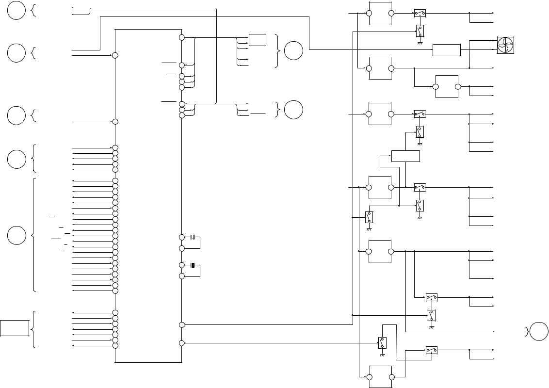
HCD-LV80
– MAIN (2/2) SECTION –
N
VIDEO
SECTION
(Page 24)
H
POWER
SECTION
(Page 25)
P
VIDEO
SECTION
(Page 24)
C
BD
SECTION
(Page 20)
B
DECK
SECTION
(Page 21)
FM/AM TUNER
TUNER UNIT IS SUPPLED AS THE ASSEMBLED BLOCK
09
|
|
|
|
|
|
|
|
|
|
|
|
IC931 |
Q931 |
|
|
|
|
|
|
|
|
|
|
|
|
|
|
|
|
|
|
|
|
I2C CLK |
29 |
|
|
|
|
|
|
|
|
|
|
+10V |
SWITCH |
|
|
|
I2C DATA |
30 |
|
|
|
|
|
|
|
|
+UNREG, 17V |
1 |
3 |
|
|
|
|
|
|
|
|
|
|
|
|
REG |
|
|
|
|||||
|
|
|
|
|
|
|
|
|
|
|
|
|||||
|
|
|
MAIN CONTROL |
|
|
|
|
|
|
|
|
|
|
|
|
|
|
|
|
IC501 (2/2) |
|
|
|
|
|
|
|
|
2 |
Q932 |
|
|
|
|
|
|
|
|
|
|
|
LX7 |
|
|
|
|
|
|
||
|
|
|
|
|
|
1 |
43 |
|
|
|
|
|
SWITCH |
|
||
|
|
|
|
STK-POWER |
1 |
POWER |
|
|
|
|
|
|
||||
|
|
|
|
|
|
|
|
|
|
|
|
|||||
|
|
|
|
|
42 |
|
|
|
|
|
|
|
|
|||
|
|
|
|
|
|
|
ECO |
|
|
|
|
|
|
|
|
|
|
|
|
|
|
|
|
93 |
I |
|
|
|
|
FAN SWITCH |
|
||
FAN DET |
|
|
|
|
|
|
HP MUTE |
|
|
|
|
|
||||
|
|
|
|
|
|
|
|
|
|
|
|
|||||
|
|
|
|
|
|
|
|
|
|
IC932 |
|
|
Q961, 963 |
|
||
HP.SW |
|
36 |
H/P IN |
|
|
|
|
|
|
|
|
|
|
|||
|
|
|
|
1 |
|
|
|
|
|
|
|
|||||
|
|
|
|
STK POWER |
|
|
|
|
|
|
|
|||||
|
|
|
|
|
|
27 |
27 |
|
|
|
|
|
|
|
|
|
|
|
|
|
PROTECT |
27 |
PROTECT |
POWER |
|
|
+12V |
|
|
|
|
||
|
|
|
|
|
|
|
1 |
3 |
|
|
|
|||||
|
|
|
|
|
|
42 |
|
|
SECTION |
|
REG |
|
IC933 |
|
||
|
|
|
|
FL OFF |
42 |
|
|
(Page 25) |
|
|
|
|
|
|
||
|
|
|
|
43 |
|
|
|
|
|
|
|
|
|
|||
|
|
|
|
|
|
|
|
|
|
|
|
|
|
|
||
|
|
|
|
STBY RELAY |
43 |
93 |
|
|
|
|
|
|
|
|
+7V |
|
|
|
|
|
HP MUTE |
93 |
|
|
|
|
|
|
|
1 |
3 |
||
|
|
|
|
|
|
|
|
|
|
|
|
REG |
||||
|
|
|
|
|
|
|
|
|
|
|
|
|
|
|
|
|
|
|
|
|
WAKE UP |
18 |
18 |
30 |
DATA |
J |
|
|
IC951 |
Q903 |
|
|
|
|
|
|
|
|
|
|
|
|
|
|||||||
|
|
|
|
29 |
29 |
|
|
|
SWITCH |
|
|
|||||
|
|
|
|
IIC-CLK |
29 |
CLOCK |
UN–12V |
|
–7V |
|
|
|||||
|
|
|
|
30 |
18 |
2 |
3 |
|
|
|
||||||
|
|
|
|
IIC-DATA |
30 |
WAKE UP |
|
|
|
|||||||
|
|
|
|
|
|
REG |
|
|
|
|||||||
X-RST |
|
59 |
XRST |
|
|
|
|
|
DISPLAY |
|
|
|
|
|
|
|
|
|
|
|
|
|
|
|
|
|
|
|
|
|
|
|
|
|
|
|
|
|
|
|
|
|
SECTION |
|
|
|
|
Q904 |
|
|
|
|
|
|
|
|
|
|
|
(Page 26) |
|
|
|
|
SWITCH |
|
|
|
|
|
|
|
|
|
|
|
|
|
|
|
|
|
|
|
TRAY.SENS |
|
61 |
DISC-SENS |
|
|
|
|
|
|
|
|
|
|
|
|
|
TBL.L |
|
63 |
TBL-L |
|
|
|
|
|
|
|
|
|
DETECTOR |
|
|
|
TBL.R |
|
65 |
TBL-R |
|
|
|
|
|
|
|
|
|
Q905 |
|
|
|
UP SW |
|
68 |
ENC 3/UP-SW |
|
|
|
|
|
|
|
|
|
|
|
|
|
LED |
|
69 |
ENC 2/DISC-LED |
|
|
|
|
|
|
|
|
IC901 |
|
|
|
|
|
|
|
|
|
|
|
|
|
|
|
|
Q911 |
|
|
|
|
|
|
|
|
|
|
|
|
|
|
|
|
|
|
|
|
|
B TRG |
|
72 |
B-TRG |
|
|
|
|
|
|
|
|
+7V |
SWITCH |
|
|
|
A TRG |
|
73 |
A-TRG |
|
|
|
|
|
|
UN+12V |
1 |
3 |
|
|
|
|
CAPM-CNT 2 |
|
74 |
CAPM-CNT 2 |
|
|
|
|
|
|
REG |
|
|
|
|||
|
|
|
|
|
|
|
|
|
|
|
|
|
||||
|
|
|
|
|
|
|
|
|
|
|
|
|
(LED+7V) |
|||
CAPM-CNT 1 |
|
75 |
CAPM-CNT 1 |
|
|
|
|
|
|
|
|
|
|
|
|
|
|
|
|
|
|
|
|
|
|
|
2 |
|
|
|
|||
CAP-M-H/L |
|
76 |
CAP-M-H/L |
|
|
|
|
|
|
|
|
|
Q912 |
|
|
|
MS OUT |
|
77 |
AMS IN |
|
|
|
|
|
|
|
|
|
|
SWITCH |
|
|
LM ON/OFF |
|
78 |
TC-MUTE |
|
|
|
|
|
|
|
Q902 |
|
|
|
|
|
REC/PB/PASS |
|
79 |
R/PB/PAS |
|
|
|
|
|
|
|
SWITCH |
|
|
|
|
|
NR ON/OFF |
|
80 |
NR-ON/OFF |
|
|
X501 |
|
|
|
|
|
|
|
|
|
|
RM ON/OFF |
|
81 |
REC-MUTE |
|
|
|
|
|
|
|
|
|
|
|
|
|
|
|
|
32.768kHz |
|
|
|
|
|
|
|
|
|
|
|||
BIAS ON/OFF |
|
82 |
BIAS |
|
|
|
|
|
|
|
|
|
|
|
|
|
|
XC-IN |
10 |
|
|
|
|
|
|
IC911 |
|
|
|
|
|||
NORM/HIGH |
|
83 |
EQ-H/N |
|
|
|
|
|
|
|
|
|
|
|||
|
|
|
|
|
|
|
|
|
|
|
|
|
|
|||
PB A/B |
|
84 |
PB-A/B |
XC-OUT |
11 |
|
|
|
|
|
1 |
+5V |
3 |
|
|
|
ALC ON/OFF |
|
85 |
ALC |
|
|
|
|
|
|
|
|
|||||
|
|
|
X502 |
|
|
|
|
REG |
|
|
|
|||||
B PLAY |
|
86 |
B-PLAY-SW |
|
|
|
|
|
|
|
|
|
|
|
||
|
|
|
|
|
|
|
|
|
|
|
|
|
||||
|
|
|
16MHz |
|
|
|
|
|
|
|
|
|
|
|||
A PLAY |
|
87 |
A-PLAY-SW |
X-OUT |
13 |
|
|
|
|
|
|
|
|
|
|
|
|
|
|
|
|
|
|
|
|
|
|
|
|||||
A-HALF |
|
88 |
A-HALF |
|
|
|
|
|
|
|
|
|
|
|
||
|
|
|
|
|
|
|
|
|
|
|
|
|
|
|||
B-HALF/REC A/REC B |
|
89 |
B-HALF |
X-IN |
15 |
|
|
|
|
|
|
|
|
|
|
|
B SHUT |
|
90 |
B-SHUT |
|
|
|
|
|
|
|
|
|
|
|
||
|
|
|
|
|
|
|
|
|
|
|
|
|
|
|||
A SHUT |
|
91 |
A-SHUT |
|
|
|
|
|
|
|
|
|
|
Q911 |
|
|
RELAY |
|
100 |
TC-RELAY |
|
|
|
|
|
|
|
|
|
|
SWITCH |
|
(D+5V SW) |
|
|
|
|
|
|
|
|
|
|
|
|
|
|
|
|
|
ST-MUTE |
|
49 |
ST-MUTE |
|
|
|
|
|
|
|
|
|
2 |
Q912 |
|
|
STEREO |
|
50 |
STEREO |
|
|
|
|
|
|
|
|
|
|
SWITCH |
|
|
TUNED |
|
51 |
TUNED |
POWER |
2 |
|
|
|
|
|
Q914 |
|
|
|
|
|
ST-CE |
|
52 |
ST-CE |
|
|
|
|
|
|
|
|
|
|
|
||
ST-DOUT |
|
53 |
ST-DOUT |
|
|
|
|
|
|
|
SWITCH |
|
Q913 |
|
|
|
|
|
|
|
|
|
|
|
5 |
|
|
|
|
||||
ST-DIN |
|
54 |
ST-DIN |
CD-POWER |
5 |
|
|
|
|
|
|
|
|
|
||
ST-CLK |
|
55 |
ST-CLK |
|
|
|
|
|
|
|
|
SWITCH |
|
(CD D+5V SW) |
||
|
|
|
|
|
|
|
|
|
|
|
|
|
||||
|
|
|
|
|
|
|
|
|
|
|
|
IC921 |
|
|
|
(CD A+5V SW) |
|
|
|
|
|
|
|
|
|
|
|
1 |
+5V |
3 |
|
|
|
|
|
|
|
|
|
|
|
|
|
|
REG |
|
|
|
||
|
|
|
|
|
|
|
|
|
|
|
|
|
|
|
|
|
• R CH : Same as L ch |
|
|
|
|
|
|
|
|
|
|
|
|
|
|
|
|
|
|
|
|
|
|
|
|
|
|
23 |
23 |
|
|
|
|
|
PL A+10V
ST +10V
M901
FAN
TC MOTOR+12V
M+7V (UNSW)
7V
ST A-7V
LED-7V
TC–7V
–7V
ST A+7V
LED+7V
TC+7V
+7
LED 5V
EVER +5V
D+5V UNSW
5V
AU D+5V
EVER +5V
D+5V (SW)
A+5V (SW)
L
POWER
SECTION
(Page 25)
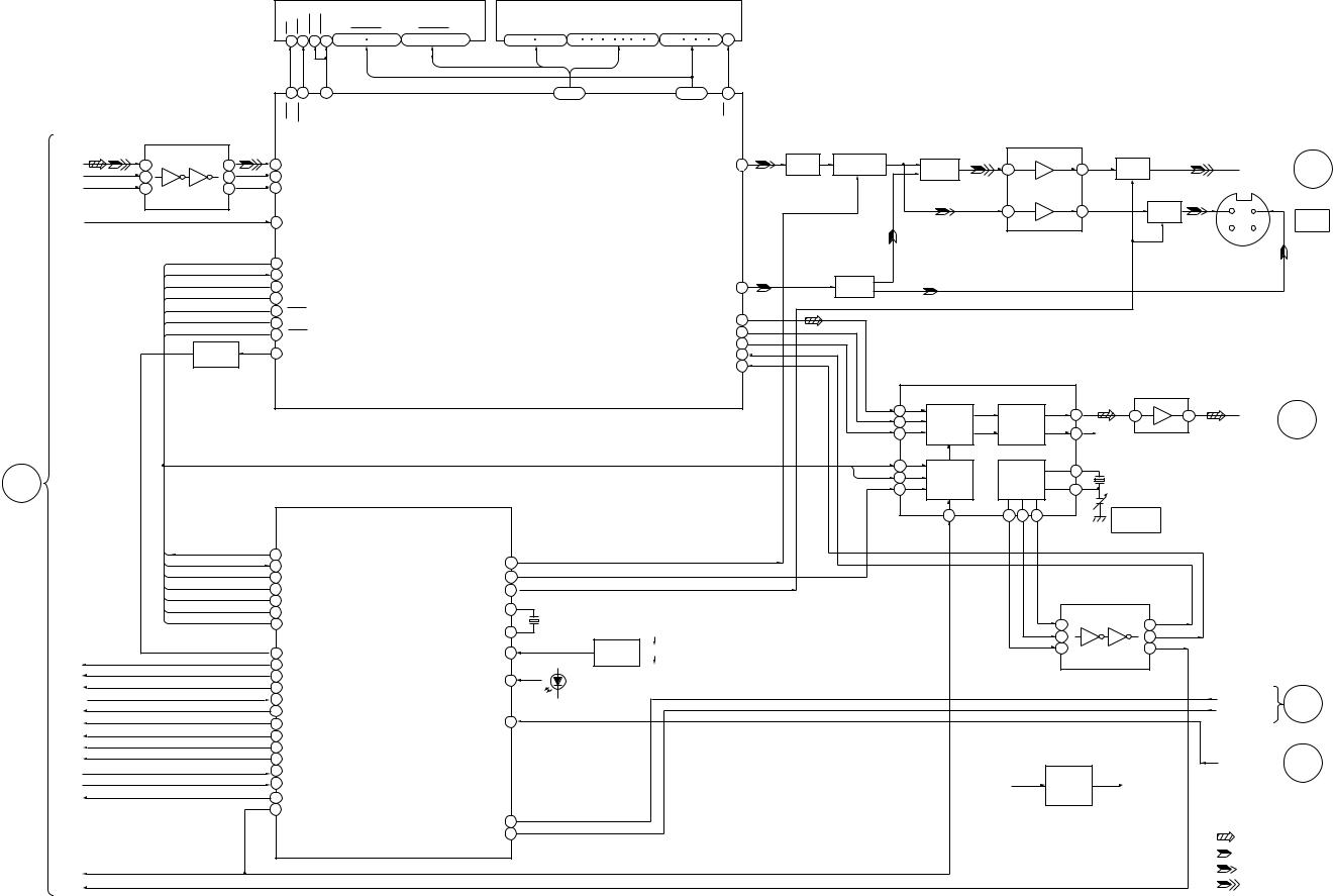
HCD-LV80
– VIDEO SECTION –
|
|
D-RAM |
|
|
IC507 |
WE RAS UCAS LCAS |
A0 |
A8 |
13 14 28 29 |
16 - 19 |
22 - 26 |
DQ1 2
DQ16 - 10  31 - 39
ROM
IC506
O0 |
|
|
O7 |
A11 |
|
A17 |
A0 |
|
A10 |
|
CE |
13 - 15 |
17 - 21 |
25 4 28 29 3 2 14 10 |
12 - 5 27 26 23 |
22 |
|||||||
38 42 |
40 |
10 - 29 |
58 - 44 |
37 |
MWE RASO |
CAS |
MD0 I MD15 |
MA0 I MA10 |
MCE |
|
|
|
LEVEL SHIFT |
|
|
|
|
|
|
|
|
|
|
|
|
OUTPUT AMP |
|
|
|
|
|
|
|
|
|
|
|
IC501 |
|
|
|
|
|
|
|
|
|
|
|
|
|
|
|
|
|
|
|
||
|
|
|
|
|
|
|
|
|
|
|
|
|
|
|
|
IC401 |
|
|
|
|
|
|
|
|
|
|
|
|
|
|
|
|
|
|
|
|
|
|
|
|
|
|
|
|
|
|
|
|
|
|
ADATA |
1 |
4 |
4 |
CD-DATA |
|
|
|
|
Y-OUT |
69 |
BUFFER |
TRAP |
|
MIX AMP |
|
|
MUTE |
|
|
|
|
O |
MAIN (1/2) |
|
|
|
|
|
|
|
7 |
|
|
|
|
SECTION |
||||||||||||
|
|
|
|
|
Q301 |
Q302,306,307 |
|
5 |
|
|
VCD VIDEO |
|||||||||||||
|
BCLK |
13 |
10 |
3 |
CD-BCK |
|
|
|
|
|
|
|
Q308,310 |
Q454 |
|
|
||||||||
|
|
|
|
|
|
|
|
|
|
|
|
|
|
|
|
(Page 22) |
||||||||
|
|
|
|
|
|
|
|
|
|
|
|
|
|
|
|
|
|
|||||||
|
LRCK |
5 |
8 |
5 |
CD-LRCK |
|
|
|
|
|
|
|
|
|
|
|
|
|
|
|
|
|
|
|
|
|
|
|
|
|
|
|
|
|
|
|
|
|
|
|
3 |
1 |
|
MUTE |
|
|
|
J301 |
|
|
|
|
|
|
|
|
|
|
|
|
|
|
|
|
|
|
4 |
|
|
S VIDEO |
|
|||
|
|
|
|
|
|
|
|
|
|
|
|
|
|
|
|
|
Q453 |
3 |
|
|
||||
|
C2P0 |
|
|
6 |
CD-C2P0 |
|
|
|
|
|
|
|
|
|
|
|
|
|
|
|
||||
|
|
|
|
|
|
|
|
|
|
|
|
|
|
|
|
|
|
|
|
OUT |
|
|||
|
|
|
|
|
|
VIDEO/CD DECODER |
|
|
|
|
|
|
|
|
|
|
|
|
2 |
1 |
|
|
||
|
|
|
|
|
|
|
|
|
|
|
|
|
|
|
|
|
|
|
|
|
||||
|
|
|
|
|
|
|
IC505 |
|
|
|
|
|
|
|
|
|
|
|
|
|
|
|
|
|
|
|
|
DATAI |
112 |
HD-OUT |
|
|
|
|
|
|
|
|
|
|
|
|
|
|
|
|
|
|
|
|
|
|
DATAO |
|
|
|
|
|
|
|
|
|
|
|
|
|
|
|
|
|
|
|
||
|
|
|
119 |
HD-IN |
|
|
|
|
|
|
|
|
|
|
|
|
|
|
|
|
|
|
|
|
|
|
|
CLK1 |
|
|
|
|
|
|
|
BUFFER |
|
|
|
|
|
|
|
|
|
|
|
||
|
|
|
117 |
HCK |
|
|
|
|
C-OUT |
75 |
|
|
|
|
|
|
|
|
|
|
|
|
||
|
|
|
HRDY |
|
|
|
|
|
Q303,304 |
|
|
|
|
|
|
|
|
|
|
|
||||
|
|
|
113 |
HRDY |
|
|
|
|
|
|
|
|
|
|
|
|
|
|
|
|
|
|
||
|
|
|
INT |
|
|
|
|
|
|
|
|
|
|
|
|
|
|
|
|
|
|
|
||
|
|
|
114 |
HINT |
|
|
|
|
|
|
|
|
|
|
|
|
|
|
|
|
|
|
|
|
|
|
|
HSEL |
|
|
|
|
DA-DATA |
110 |
|
|
|
|
|
|
|
|
|
|
|
|
|
||
|
|
|
121 |
HSEL |
|
|
|
|
|
|
|
|
|
|
|
|
|
|
|
|
|
|||
|
|
|
RST |
|
|
|
|
|
|
|
|
|
|
|
|
|
|
|
|
|
||||
|
|
|
60 |
RESET |
|
|
|
|
DA-LRCK |
108 |
|
|
|
|
|
|
|
|
|
|
|
|
|
|
|
|
|
|
|
|
|
|
|
|
|
|
|
|
|
|
|
|
|
|
|
||||
|
|
|
INVERTER |
93 |
PGIO2/VSYNC/CSYNC |
|
|
|
|
DA-BCK |
111 |
27MHz |
|
|
|
|
|
|
|
|
|
|
|
|
|
|
|
|
|
|
|
VCK-IN |
106 |
|
|
|
|
|
|
|
|
|
|
|
|
||||
|
|
|
Q502 |
|
|
|
|
|
|
DA-XCLK |
86 |
|
|
|
DIGITAL FILTER & D/A CONVERTER |
|
|
|
|
|
|
|
|
|
|
|
|
|
|
|
|
|
|
|
|
|
|
|
|
|
|
|
|
|
|
||||
|
|
|
|
|
|
|
|
|
|
|
|
|
|
|
IC509 |
|
|
|
AMP |
|
|
|
|
|
|
|
|
|
|
|
|
|
|
|
|
|
|
|
|
|
|
|
|
|
|
|
|
|
|
|
|
|
|
|
|
|
|
|
|
|
|
|
|
|
|
|
|
|
IC101 |
|
|
|
|
|
|
|
|
|
|
|
|
|
|
|
|
|
|
|
18 |
D/A |
|
14 |
3 |
|
1 |
CD-L |
|
M |
|
|
|
|
|
|
|
|
|
|
|
|
|
|
|
19 |
PLM |
|
(L - CH) |
|
|
|||||
|
|
|
|
|
|
|
|
|
|
|
|
|
|
|
|
|
|
|
|
|||||
|
|
|
|
|
|
|
|
|
|
|
|
|
|
17 |
CONV |
|
11 |
R-CH |
|
|
|
|
|
|
|
|
|
|
|
|
|
|
|
|
|
|
|
|
|
|
|
|
|
|
|
MAIN (1/2) |
|
||
|
|
|
CLK1, DATA0 |
|
|
|
|
|
|
|
|
|
DATA0 |
9 |
|
|
|
|
|
|
|
SECTION |
|
|
A |
|
|
|
|
|
|
|
|
|
|
|
|
CLK1 |
MODE |
CLOCK |
1 |
X503 |
|
|
(Page 22) |
|
|||
|
|
|
|
|
|
|
|
|
|
|
|
8 |
|
|
|
|||||||||
|
|
|
|
|
|
|
|
|
|
|
|
|
|
|
|
|
|
|
|
|
|
|
||
|
|
|
|
|
VIDEO CD CONTROL |
|
|
|
|
|
|
|
7 |
|
DIVIDER |
24 |
27MHz |
|
|
|
|
|
|
|
|
|
|
|
|
|
|
|
|
|
|
|
|
|
|
|
|
|
|
|
|||||
|
|
|
|
|
|
|
|
|
|
|
|
|
|
|
|
|
|
|
|
|
||||
|
|
|
|
|
|
IC502 |
|
|
|
|
|
|
|
|
|
|
|
CT503 |
|
|
|
|
|
|
CD |
|
|
|
|
|
|
|
|
|
|
|
|
|
|
|
|
|
|
|
|
|
|
|
|
|
|
|
|
|
|
|
|
|
|
|
|
|
|
10 |
21 20 |
4 |
VIDEO |
|
|
|
|
|
|
|
SECTION |
|
|
|
|
|
|
|
|
|
|
|
|
|
|
|
|
|
|
|
|
||||
|
|
|
|
|
|
|
|
|
|
|
|
|
|
RSTB |
|
|
FREQUENCY |
|
|
|
|
|
||
(Page 20) |
|
|
|
|
|
|
|
|
|
|
|
|
|
|
|
|
|
|
|
|
|
|||
|
|
|
|
|
|
|
|
|
|
|
|
|
|
|
|
|
|
|
|
|
|
|
|
|
|
|
|
DATA0 |
31 |
DATA1O |
|
|
|
|
|
|
|
|
|
|
|
|
|
|
|
|
|
|
|
|
|
|
DATAI |
SHARPNESS |
34 |
|
|
|
|
|
|
|
|
|
|
|
|
|
|
|
|
|
||
|
|
|
32 |
DATA1I |
|
|
|
|
|
|
|
|
|
|
|
|
|
|
|
|
|
|||
|
|
|
CLK1 |
|
|
|
|
|
|
|
|
|
|
|
|
|
|
|
|
|
|
|
||
|
|
|
33 |
CLK1 |
DF LATCH |
22 |
|
|
|
|
|
|
|
|
|
|
|
|
|
|
|
|
|
|
|
|
|
INT |
|
|
|
|
|
|
|
|
|
|
LEVEL SHIFT |
|
|
|
|
|
|
||||
|
|
|
20 |
CL680 INT |
A7 |
65 |
|
|
|
|
|
|
|
|
|
|
|
|
|
|
|
|
||
|
|
|
HSEL |
|
|
|
|
|
|
|
|
|
|
|
|
|
|
|
|
|||||
|
|
|
21 |
CL680 HSEL |
|
|
|
|
|
|
|
|
|
|
|
|
IC504 |
|
|
|
|
|
|
|
|
|
|
HRDY |
XIN |
15 |
|
|
|
|
|
|
|
|
|
|
|
|
|
|
|
|
|
||
|
|
|
23 |
CL680 HRDY |
X501 |
|
|
|
|
|
|
|
|
|
|
|
|
|
|
|
|
|||
|
|
|
RESET |
|
|
|
|
|
|
|
|
|
|
|
|
27MHz |
|
|
|
|
|
|||
|
|
|
24 |
680 RESET |
|
|
|
|
|
|
|
|
|
|
3 |
6 |
|
|
|
|
|
|||
|
|
|
|
|
10MHz |
|
|
|
|
|
|
|
|
|
|
|
|
|
||||||
|
|
|
|
|
13 |
|
NTSC |
|
|
|
|
|
|
|
|
|
|
|
||||||
|
|
|
|
|
|
XOUT |
|
S501 |
|
|
|
|
|
|
11 |
8 |
384FS |
|
|
|
|
|
||
|
|
|
|
45 |
BUS |
NT/PAL |
93 |
|
SYSTEM |
AUTO |
|
|
|
|
|
|
1 |
12 768FS |
|
|
|
|
|
|
|
|
|
|
+5V |
SELECT |
|
|
|
|
|
|
|
|
|
|
|
|
|
|
|||||
|
DATA |
|
|
3 |
DSP DATA |
|
|
|
|
|
|
|
|
|
|
|
|
|
|
|
|
|
||
|
|
|
|
|
|
PAL |
|
|
|
|
|
|
|
|
|
|
|
|
|
|
||||
|
|
|
|
|
|
|
|
|
|
|
|
|
|
|
|
|
|
|
|
|
||||
|
XLT |
|
|
4 |
DSP LATCH |
|
|
|
|
|
|
|
|
|
|
|
|
|
|
|
|
|
|
|
|
|
|
TEST LED |
73 |
|
D502 |
|
|
|
|
|
|
|
|
|
|
|
|
|
|
|
|||
|
CLK |
|
|
5 |
DSP CLK |
|
|
|
|
|
|
|
|
|
|
|
|
|
|
|
MAIN (2/2) |
|||
|
|
|
|
|
|
|
|
|
|
|
|
|
|
|
|
|
|
|
|
N |
||||
|
SENS |
|
|
1 |
SENSE |
|
|
|
|
|
|
|
|
|
|
|
|
|
|
I2C.DATA |
|
|||
|
|
|
|
|
|
|
|
|
|
|
|
|
|
|
|
|
|
SECTION |
||||||
|
SCLK |
|
|
2 |
SENSE CLK |
|
|
|
|
|
|
|
|
|
|
|
|
|
|
I2C.CLK |
|
(Page 23) |
||
|
|
|
|
XRESET |
12 |
|
|
|
|
|
|
|
|
|
|
|
|
|
|
|
||||
|
MUTE |
|
|
10 |
DSP MUTE |
|
|
|
|
|
|
|
|
|
|
|
|
|
|
|
|
|||
|
CTRL1 |
|
|
11 |
CTRL1(L:DOUBLE) |
|
|
|
|
|
|
|
|
|
|
|
|
|
|
|
|
|
|
|
|
LPH |
|
|
27 |
CTRL2 |
|
|
|
|
|
|
|
|
|
|
|
|
|
|
|
|
|
P |
MAIN (2/2) |
|
LDON |
|
|
28 |
LDON |
|
|
|
|
|
|
|
|
|
|
|
|
|
|
X-RST |
|
|
SECTION |
|
|
|
|
|
18 |
SCOR |
|
|
|
|
|
|
|
|
|
|
|
|
|
|
|
|
|||
|
SCOR |
|
|
|
|
|
|
|
|
|
|
|
|
D5V |
3.3V REG |
+3.3V |
|
|
|
|
(Page 23) |
|||
|
SUBQ |
|
|
36 |
SUBQ DATA |
|
|
|
|
|
|
|
|
|
|
|
|
|
|
|
|
|||
|
SQCK |
|
|
37 |
SUBQ CLK |
|
|
|
|
|
|
|
|
|
|
|
Q531 |
|
|
|
|
|
|
|
|
|
|
|
|
|
|
|
|
|
|
|
|
|
|
|
|
• R CH: Same as L ch |
|
||||||
|
|
|
|
77 |
DEVICE RESET |
|
|
|
|
|
|
|
|
|
|
|
|
|
|
|
||||
|
|
|
|
|
|
|
|
|
|
|
|
|
|
|
|
|
|
• SIGNAL PATH |
|
|
|
|||
|
|
|
|
|
|
I2C.DATA |
30 |
|
|
|
|
|
|
|
|
|
|
|
|
|
|
|
||
|
|
|
|
|
|
I2C.CLK |
29 |
|
|
|
|
|
|
|
|
|
|
|
|
|
: CD |
|
|
|
|
|
|
|
|
|
|
|
|
|
|
|
|
|
|
|
|
|
|
|
|
|
|
|
|
|
|
|
|
|
|
|
|
|
|
|
|
|
|
|
|
|
|
|
|
|
: CHROMA |
|
||
|
XRST |
(XTAL 33.8MHz) |
|
|
|
|
|
|
|
|
|
|
|
|
|
|
|
|
|
|
:Y |
|
|
|
|
|
|
|
|
|
|
|
|
|
|
|
|
|
|
|
|
|
|
|
: VIDEO |
|
|
|
|
09 |
MCK |
|
|
|
|
|
|
|
|
|
|
|
|
|
|
|
|
|
|
|
|
|
|
|
|
|
|
|
|
|
|
|
|
24 |
24 |
|
|
|
|
|
|
|
|
|
|
|
|
|
|
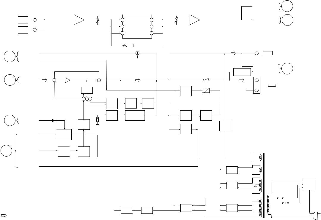
– POWER SECTION –
|
|
|
|
|
MIC-SIG |
MIC AMP |
MIC LEVEL |
ECHO CONTROL |
ECHO LEVEL |
MIC AMP |
|
IC850 (1/2) |
RV750 |
|
IC851 |
RV751 |
IC850 (2/2) |
J801 |
|
|
|
|
|
MIC 1 |
1 |
LPF 1 IN |
LPF 1 OUT |
2 |
MIC-SIG |
J802 |
9 |
LPF 2 IN |
LPF 2 OUT |
8 |
|
MIC 2 |
|
|
|
|
|
|
11 |
OP 2 IN |
OP 2 OUT |
10 |
|
HCD-LV80
K |
DISPLAY |
SECTION |
|
(Page 26) |
|
Q |
MAIN (1/2) |
SECTION |
|
(Page 22) |
|
|
|
|
|
|
|
|
|
J803 |
|
|
MAIN (1/2) |
G |
DBFB |
|
|
|
|
|
|
|
PHONES |
|
SECTION |
|
|
|
|
|
|
|
|
|
|
|
(Page 22) |
F-RELAY |
|
|
|
|
R-ch |
|
|
|
MAIN (2/2) |
|
|
|
|
POWER AMP & VOLUME CONTROL |
|
|
|
HP.SW |
H |
|||
|
|
|
|
|
|
SECTION |
|||||
|
|
|
IC801 |
|
|
|
|
FAN DETECTOR |
FAN DET |
(Page 23) |
|
|
|
|
|
|
|
|
|
||||
|
|
|
|
|
|
|
|
D405 |
TM401 |
|
|
MAIN (1/2) |
E |
|
|
|
|
|
|
RY401 |
|
|
|
|
|
|
|
|
|
|
|
|
|||
SECTION |
L-CH IN |
18 |
|
11 |
|
|
|
|
L |
|
|
(Page 22) |
|
|
|
|
|
|
|
|
FRONT |
|
|
|
|
|
VOLUME |
|
RELAY |
R-CH |
|
R |
|
||
|
|
|
|
DRIVER |
|
|
|||||
|
|
|
CONTROL |
|
|
|
|||||
|
|
|
|
Q401-402 |
|
|
|
|
|||
|
|
|
|
|
|
|
|
|
|
|
|
|
|
|
6 |
3 |
4 |
PROTECT |
LATCH |
|
|
|
|
|
|
|
|
|
VOLUME |
|
|
|
|
||
|
|
|
|
|
CONTROL |
DC AMP |
DRIVER |
|
|
|
|
|
|
|
|
|
D802, 852 |
Q433-434 |
Q432 |
|
|
|
|
|
|
|
|
|
THERMAL |
L-CH THERMAL |
|
LATCH |
PROTECT |
|
|
|
|
MAIN (2/2) |
L |
|
D804 |
|
SENSOR |
PROTECT SWITCH |
|
DRIVER |
SWITCH |
|
|
|
|
|
|
Q831-832 |
|
Q801 |
|
Q437 |
Q431 |
|
|
|
|||
SECTION |
EVER +5V |
|
|
|
|
|
|
|
|||||
|
MUTE |
TH831 |
|
|
|
|
|
|
|
|
|||
(Page 23) |
|
|
|
|
|
|
|
|
MUTE |
|
|
||
|
|
CONTROL |
|
|
|
|
PROTECT |
|
|
|
|||
|
|
|
|
Q834 |
|
|
|
|
|
SW |
|
|
|
|
|
|
|
|
|
|
|
SWITCH |
|
Q805 |
|
|
|
|
|
|
HEAD PHONE |
|
|
|
|
|
|
|
|
||
|
|
|
|
|
|
|
|
Q439 |
|
|
|
|
|
|
|
HP-MUTE |
MUTE |
|
|
|
|
|
|
|
|
|
|
|
|
|
Q833 |
|
|
|
|
|
|
|
|
|
|
MAIN (2/2) |
I |
|
|
|
|
|
|
|
|
|
|
POWER |
|
|
MUTE |
MUTE |
|
|
|
|
|
|
|
TRANSFORMER |
|
||
SECTION |
STK-POWER |
DRIVE |
SWITCH |
|
|
|
|
|
|
|
T951 |
|
|
(Page 23) |
|
Q804 |
Q803 |
|
|
|
|
|
|
|
VF |
|
|
|
|
|
|
|
|
|
|
|
|
|
|
VF |
|
|
|
PROTECT |
|
|
|
|
|
|
|
+UNREG. 12V |
RECT |
|
|
|
|
|
|
|
|
|
|
|
|
|
|
||
|
|
|
|
|
|
|
|
|
|
D833-836 |
|
|
|
|
|
|
|
|
|
|
|
|
|
|
|
|
|
|
|
|
|
|
|
|
|
|
|
|
|
240V |
|
|
|
|
|
|
|
|
|
|
|
UN +10V |
RECT |
|
VOLTAGE |
|
|
|
|
|
|
|
|
|
|
|
SELECTOR |
||
|
|
|
|
|
|
|
|
|
|
|
|
||
|
|
|
|
|
|
|
|
|
|
UN –10V |
D841-844 |
|
VS901 |
|
|
|
|
|
|
|
|
|
|
|
|
230V |
JW971 |
|
|
|
|
|
|
|
|
|
|
|
|
|
|
• R CH : Same as L ch |
|
|
|
|
|
|
|
|
|
120V |
|
||
|
|
|
|
|
+VH |
RECT |
AC-L |
RECT |
|
F951 |
|||
|
|
|
|
|
|
SWITCH |
–35V REG |
|
|
|
|
||
• SIGNAL PATH |
|
|
|
VF (–35V) |
|
D831 |
AC-L |
D832 |
|
|
|||
|
|
|
|
Q908 |
Q903 |
|
|
|
|
|
AC |
||
09 |
: FM |
|
|
|
|
|
|
|
|
|
|
|
|
|
|
|
|
|
|
|
|
|
|
|
IN |
||
|
|
|
|
|
|
|
|
|
|
|
|
||
25 25
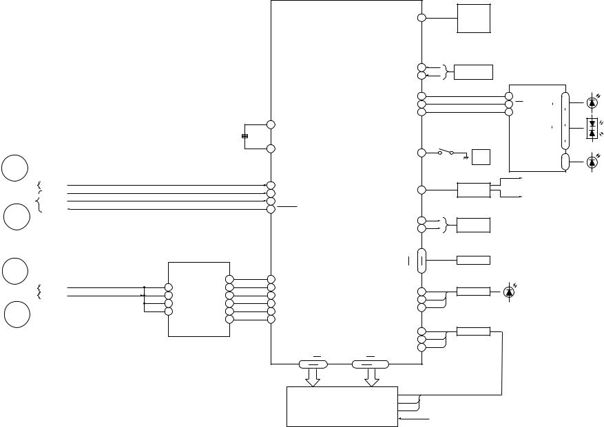
HCD-LV80
– DISPLAY SECTION –
(Page22) |
F |
|
|
|
|
|
MAIN (1/2) SECTION |
|
|
|
|
|
|
|
RESET |
|||||
MAIN (2/2) SECTION |
|
|
|
DATA |
||
|
||||||
|
|
CLOCK |
||||
(Page |
J |
|
|
|||
|
|
|
||||
|
WAKE UP |
|||||
|
|
|
|
|
||
23) |
|
|
|
|
|
|
(Page 25) |
|
|
|
|
|
|
|
K |
|
|
|
|
|
POWER SECTION |
|
|
MIC–SIG |
|||
MAIN (1/2) SECTION |
|
|
SPEANA |
|||
D
(Page 22)
09
DISPLAY CONTROL
IC601
|
|
|
|
|
|
|
|
REMOTE |
|
|
|
|
|
|
|
|
|
SIRCS |
1 |
CONTROL |
|
|
|
|
|
|
|
|
|
RECIEVE |
|
|
|
||
|
|
|
|
|
|
|
|
|
|
|
|
|
|
|
|
|
|
|
|
IC702 |
|
|
|
|
|
|
|
|
|
|
|
S701 |
|
|
|
|
|
|
|
|
|
|
|
JOG |
SERIAL |
|
|
|
|
|
|
|
|
JOG A |
2 |
.AMS > |
PARALLEL |
|
|
|
|
|
|
|
|
JOG B |
8 |
CONVERTER |
|
||
|
|
|
|
|
|
|
IC701 |
|
|
||
|
|
|
|
|
|
|
|
|
|
|
|
|
|
|
|
|
|
LED SCK |
3 |
|
14 CLK |
P3 |
1 |
|
|
|
|
|
|
LED LATCH |
4 |
|
15 STB |
• |
|
|
|
|
|
|
|
|
P5 |
3 |
|||
|
|
|
|
|
|
LED DAT |
5 |
|
13 DATA |
• |
5 |
|
|
|
|
|
|
|
|
|
|
P7 |
• |
|
|
|
|
|
|
|
|
|
|
• |
|
|
|
|
70 X IN |
|
|
|
|
|
|
7 |
|
|
|
|
|
|
|
|
|
|
P9 |
11 |
|
|
|
X601 |
|
|
|
|
|
|
|
P16 |
|
|
|
|
|
|
|
|
|
|
• |
||
|
|
12.5MHz |
|
|
|
|
|
|
|
|
20 |
|
|
|
|
|
|
|
S691 |
|
|
22 |
|
|
|
|
72 X OUT |
|
|
|
|
|
|
||
|
|
|
|
|
D-SW |
80 |
Z |
|
|
|
|
|
|
|
|
|
|
|
P1 |
17 |
|||
|
|
|
|
|
|
|
|
OPEN |
|
||
|
|
|
|
|
|
|
|
|
• |
• |
|
|
|
|
|
|
|
|
|
|
|
P2 |
19 |
|
|
|
|
|
|
|
|
Q601 – Q603 |
+5VH |
|
|
|
|
|
73 RESET |
|
|
LED SEL |
7 |
LED POWER |
|
|
|
|
|
|
78 I2C DATA |
|
|
SWITCH |
+5VL |
|
|
||
|
|
|
79 I2C CLK |
|
|
|
|
|
|
|
|
|
|
|
|
|
|
|
|
|
|
|
|
|
|
|
22 WAKE UP |
|
|
|
|
S701 |
|
|
|
|
|
|
|
|
|
|
|
|
|
|
|
|
|
|
|
|
|
VOLUME A |
9 |
VOLUME |
|
|
|
|
|
|
|
|
|
VOLUME B 10 |
|
|
|
||
|
|
|
|
|
|
|
|
|
|
||
|
REC LEVEL |
|
|
|
|
|
|
|
|
|
|
|
OUTPUT |
|
|
|
|
|
|
|
|
|
|
DISPLAY CONTROL (FOR MIC) |
|
|
|
KEY 0 |
11 |
|
|
|
|
||
|
IC603 |
|
|
|
|
KEY MATRIX |
|
|
|
||
|
|
|
|
|
|
|
|
|
|
||
|
|
|
|
|
|
|
|
|
|
|
|
|
|
|
|
|
|
KEY 4 |
15 |
|
|
|
|
|
REC LEVEL 11 |
21 ALL BAND |
|
|
|
|
Q605 – Q607 |
|
|
|
|
3 |
LINE NF |
F06 12 |
20 BPF 4 |
|
|
|
|
|
|
|
|
|
|
DAILY LED |
74 |
LED DRIVER |
D601 – D603 |
|
|
||||
4 |
LINE IN |
F05 13 |
19 BPF 3 |
|
|
|
|
||||
|
|
REC LED |
75 |
|
|
|
|
||||
6 |
REC IN |
F04 14 |
18 BPF 2 |
|
|
|
|
|
|
||
|
|
LED-EC0 |
77 |
|
|
|
|
||||
5 |
REC NF |
F02 16 |
17 BPF 1 |
|
|
|
|
|
|
||
|
|
|
|
|
|
|
|
||||
|
|
F01 17 |
16 BPF 0 |
|
|
|
|
Q608 – Q610 |
|
|
|
|
|
|
|
|
|
|
|
|
|
|
|
|
|
|
|
|
|
GR-1 |
43 |
DRIVER |
|
|
|
|
|
|
|
|
|
GR-15 |
28 |
|
|
|
|
|
|
|
|
|
|
GR-16 |
27 |
|
|
|
|
|
|
|
SEG-1 |
23 |
GR-3 |
14, 2 |
|
|
|
|
|
|
|
|
45 |
67 |
29 |
40, 42 |
|
|
|
|
|
D604 – D607, D611, D612, D615 – D621,
D623 – D627, D635 – D638
D700
D631, D632, D641
FLUORESCENT INDICATOR TUBE
FL601
VF
26 26
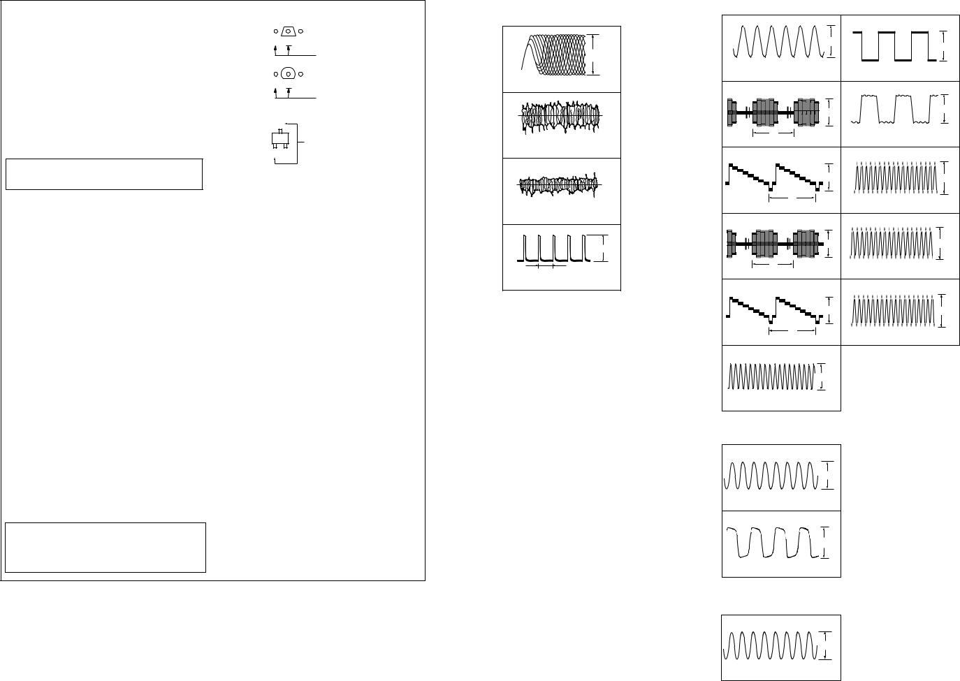
THIS NOTE IS COMMON FOR PRINTED WIRING BOARDS AND SCHEMATIC DIAGRAMS.
(In addition to this, the necessary note is printed in each block.)
For schematic diagrams.
Note:
•All capacitors are in µF unless otherwise noted. pF: µµF
50 WV or less are not indicated except for electrolytics and tantalums.
•All resistors are in Ω and 1/4 W or less unless otherwise specified.
•f : internal component.
•2: nonflammable resistor.
•1: fusible resistor.
•C: panel designation.
Note: The components identified by mark 0or dotted line with mark 0are critical for safety.
Replace only with part number specified.
•U : B+ Line.
•V : B– Line.
•H: adjustment for repair.
•Voltages and waveforms are dc with respect to ground under no-signal (detuned) conditions.
•Voltages are taken with a VOM (Input impedance 10 MΩ).
Voltage variations may be noted due to normal production tolerances.
•Waveforms are taken with a oscilloscope.
Voltage variations may be noted due to normal production tolerances.
•Circled numbers refer to waveforms.
•Signal path.
F : FM
g : VIDEO/MD E : PB (DECK A) d : PB (DECK B)
G : REC (DECK B) m : CHROMA n : Y
o: VIDEO J : CD
c : digital out
I : PHONO
•Abbreviation
EA |
: Saudi Arabia model. |
SP |
: Singapore model. |
MY |
: Malaysia model. |
For printed wiring boards.
Note:
•X: parts extracted from the component side.
•Y: parts extracted from the conductor side.
•a : Through hole.
•b: Pattern from the side which enables seeing.
(The other layers' patterns are not indicated.)
Caution:
Pattern face side: Parts on the pattern face side seen from the (Side B) pattern face are indicated.
Parts face side: Parts on the parts face side seen from the (Side A) parts face are indicated.
• Indication of transistor
B |
C |
E |
|
|
These are omitted. |
B |
C |
E |
|
|
These are omitted. |
C |
|
|
Q |
|
These are omitted |
|
|
|
B E |
|
|
WAVEFORMS
– CD SECTION –
1 |
1.3Vp-p |
IC101 t; RFAC |
2 |
2.5V |
APPROX 500mVp-p |
IC101 ra TE |
3 |
2.5V |
APPROX 200mVp-p |
IC101 el FE |
4 |
2.6Vp-p |
7.5 sec |
IC101 wg MDP |
HCD-LV80
– VIDEO SECTION –
1 |
7 |
|
|
4Vp-p |
|
|
4.6Vp-p |
|
10MHz |
44.1kHz |
|
IC502 qd XOUT |
||
IC509 ql LRCK |
||
2 |
8 |
4.8Vp-p
 1Vp-p
1Vp-p
2.11MHz
H
IC505 ug COUT |
IC509 qj BCLK |
3 |
9 |
2Vp-p |
4.8Vp-p |
H |
33.8MHz |
IC505 yl YOUT |
IC504 8 384FS |
4 |
0 |
1Vp-p |
3.8Vp-p |
H |
27MHz |
Q303 E COUT |
IC504 6 27M |
5 |
qa |
2Vp-p |
2.8Vp-p |
H |
33.8MHz |
IC401 4 YOUT |
IC504 qs |
6
5.8Vp-p
27MHz
IC509 1 XT1
– MAIN (2/3) SECTION –
1
5.5Vp-p
16MHz
IC501 qd XC-OUT
2
5.2Vp-p
32.768kHz
IC501 qa X-OUT
– PANEL FL SECTION –
1
3.4Vp-p
12.5MHz
IC601 us X OUT
27 27

HCD-LV80
7-3. PRINTED WIRING BOARD – BD SECTION –
• See page 19 for Circuit Boards Location.
(Page 32)
28 28
Loading...