


S® |
Training Manual |
|
|
|
|
CD
Changer
Models: CDP-CX235
CDP-CX270
CDP-CX335
CDP-CX400
CDP-CX450
Circuit Description and Troubleshooting
Course: A-122
Sony Service Company
A Division of Sony Electronics Inc ©2000
All Rights Reserved
Printed in U.S.A.
SisatrademarkofSonyElectronics

Circuit Description
and Troubleshooting:
Models: CDP-CX235
CDP-CX270
CDP-CX335
CDP-CX400
CDP-CX450
Prepared by: National Training Department
Sony Service Company
A Division of Sony Electronics Inc.
Course presented by _____________________________________
Date ___________________________________________________
Student Name ___________________________________________
Overall Block Diagram
Information Gathering
CD Playback
Power Supply / Display
Power Supply
Fluorescent Display
Power On
AC Power Only
Power ON
Communications IC501 - IC701
Communications IC501 - IC101
Door Motor Drive
Operation
Drive
Feedback
Tray Table Positioning
Tray Table Slots
Light Sensors
Table Motor Drive
Front Panel Rotary Encoder - Operation
Direction of Rotation
Tray Table Position Sensors
Table of Contents
3 |
Tray Table Motor Drive |
21 |
3 |
CD Location & Label Storage |
23 |
3 |
Disc Loading Drive |
27 |
5 |
Operation |
27 |
5 |
Motor Stop |
27 |
7 |
Optical Pickup |
29 |
11 |
The Laser and Lens |
29 |
11 |
Focus Coil |
29 |
11 |
Tracking Coil |
29 |
11 |
Detector Outputs |
29 |
13 |
Servo / Audio Processing Block |
31 |
15 |
Servo Block |
31 |
15 |
Sled Motor |
31 |
15 |
Focus Servo |
31 |
15 |
Tracking Servo |
33 |
17 |
Spindle Motor |
33 |
17 |
Audio Block |
33 |
|
|
|
17 |
Servo Processing |
35 |
19 |
Sled Motor Drive |
35 |
19 |
Laser |
35 |
|
|
|
19 |
Focus |
35 |
|
|
|
19 |
Tracking Servo |
35 |
|
|
Spindle Servo |
37 |
APPENDIX |
|
Audio / Display Output |
39 |
Control A Communications for Additional Features |
i |
Analog Audio Output |
39 |
Defective Discs |
iii |
Digital Output |
39 |
Troubleshooting Using the RFO Waveform |
v |
Display |
39 |
Abbreviations Used in Compact Disc Player |
vi |
Troubleshooting |
41 |
|
|
Disc Doesn’t Spin |
42 |
|
|
Servo Processing Diagram |
43 |
|
|
Focus |
44 |
|
|
Disc Won’t Spin Flowchart |
45 |
|
|
Disc Spins, But Doesn’t Read the Disc’s |
|
|
|
Table of Contents (TOC) |
47 |
|
|
RF Output |
47 |
|
|
Tracking Servo |
47 |
|
|
Disc Spins, But Does Not Read TOC Flowchart |
48 |
|
|
Spindle Servo |
49 |
|
|
No Audio |
50 |
|
|
Optical Assembly Tests |
51 |
|
|
S Curve Check |
51 |
|
|
E-F Balance Check |
51 |
|
|
RFO Level Check |
52 |
|
|

1
CD Mega Changer Product Line (USA)
|
|
|
|
|
|
|
|
|
|
|
|
|
|
Model |
Disc |
List |
|
|
|
|
|
|
|
|
|
|
|
|
Capacity |
Price |
|
Cd Mech |
|
BD Board |
List Price |
|
Optical Assembly / Part number |
List Price |
|||
|
|
|
|
|
|
|
|
|
All of these numbers sub to 8-848-379-31 |
||||
2000 |
|
|
|
|
|
|
|
|
|
|
|
|
|
CDP-CX235 |
200 |
$170.00 |
|
CDM-40B |
|
A4724029A |
$76.15 |
|
KSS-213BNK / 8-848-379-31 |
$ |
82.12 |
||
CDP-CX270 |
200 |
$1,000 |
|
CDM-40B |
|
A4699163A |
$112.01 |
|
KSS-213B / 8-848-376-01 |
$ |
82.12 |
||
CDP-CX335 |
300 |
$300.00 |
|
CDM-54-KIBD35E |
|
A4724761A |
$82.12 |
|
KSS-213BFN / 8-848-379-31 |
$ |
82.12 |
||
CDP-CX400 |
400 |
$360.00 |
|
CDM-62-K1BD35A |
|
A4724761A |
$82.12 |
|
KSM-213BFN / 8-820-026-03 * |
$ |
82.12 |
||
CDP-CX450 |
400 |
$480.00 |
|
CDM-62-K1BD35A |
|
A4724761A |
|
|
KSM-213BFN / 8-820-026-03 * |
$ |
82.12 |
||
|
|
|
|
|
|
|
|
|
*use ’CX335 manual for part number |
|
|||
1999 |
|
|
|
|
|
|
|
|
of spindle or sled motor |
|
|
||
CDP-CX225 |
200 |
$250.00 |
|
CDM-40 |
|
A4699038A |
$112.01 |
|
KSS-213B / 8-848-376-01 |
$ |
82.12 |
||
CDP-CX230 |
200 |
$300.00 |
|
CDM-40B |
|
A4724029A |
$76.16 |
|
KSS-213BNK / 8-848-379-31 |
$ |
82.12 |
||
CDP-CX270 |
200 |
$1,000 |
|
CDM-40 |
|
A4699038A |
$112.01 |
|
KSS-213B / 8-848-376-01 |
$ |
82.12 |
||
CDP-CX300 |
300 |
$360.00 |
|
CDM-54-KIBD35E |
|
A4724761A |
$82.12 |
|
KSS-213BFN / 8-848-379-31 |
$ |
82.12 |
||
CDP-CX350 |
300 |
$480.00 |
|
CDM-54-KIBD35E |
|
A4724761A |
|
|
KSS-213BFN / 8-848-379-31 |
$ |
82.12 |
||
CDP-CX691 |
300 |
|
|
CDM-54-KIBD35E |
|
A4724761A |
|
|
KSS-213BFN / 8-848-379-31 |
$ |
82.12 |
||
|
|
|
|
|
|
|
|
|
|
|
|
|
|
1998 |
|
|
|
|
|
|
|
|
|
|
|
|
|
CDP-CX210 |
200 |
|
|
CDM-40 |
|
A4699038A |
$112.01 |
|
KSS-213B / 8-848-376-01 |
$ |
82.12 |
||
CDP-CX220 |
200 |
|
|
CDM-40B |
|
A4724029A |
$76.16 |
|
KSS-213BNK / 8-848-379-31 |
$ |
82.12 |
||
CDP-CX240 |
200 |
|
|
CDM-40B |
|
A4724029A |
|
|
KSS-213BNK / 8-848-379-31 |
$ |
82.12 |
||
CDP-CX260 |
200 |
|
|
CDM-40B |
|
A4724029A |
|
|
KSS-213BNK / 8-848-379-31 |
$ |
82.12 |
||
CDP-CX270 |
200 |
|
|
CDM-40 |
|
A4699038A |
$112.01 |
|
KSS-213B / 8-848-376-01 |
$ |
82.12 |
||
CDP-CX90ES |
200 |
$1,100 |
|
CDM-40 |
|
A4699038A |
|
|
KSS-213B / 8-848-376-01 |
$ |
82.12 |
||
|
|
|
|
|
|
|
|
|
|
|
|
|
|
List Prices are as of 7/1/00

Introduction
This training manual is based upon the model CDP-CX235 CD Changer. This model is the entry changer in the “Mega” Changer product line for the year 2000. The “2” in the model number refers to the 200 disc capacity of these Changers. These 200 series models are mechanically complex so there are more CD transport and mechanical adjustments to be made.
The concepts and circuitry in this 200 disc model are similar to the 300 disc CDP-CX300 series and 400 disc CDP-CX400 series CD Changers. In these larger capacity models, the CD transport and CD mechanism use fewer parts. As a result, the higher capacity Changers require fewer adjustments.
Generally, the electrical troubleshooting procedures and test modes outlined in this training manual can be applied to all of the changer models listed for the last three years. This is because for troubleshooting purposes, they are electrically similar. Mechanically, the 200 disc Changers use one basic chassis and the 300 and 400 disc Changers use another chassis so the mechanical adjustments differ.
Model CDP-CX90ES/CDPCX-270
The model CDP-CX90ES/CDPCX-270 was carried over from the 1998 year because it was the only chassis that had the following major features:
•A video output for an on-screen display using a TV.
•A front panel jack that permitted a computer keyboard to be plugged in. This allowed the user to label or re-label each CD slot location quickly using the keyboard instead of the slower remote control.
Model CDP-CX235
The board layout of the CDP-CX235 is shown. The bulk of the electronics are on the rear main board. To its left in the vacant area is the CD mechanism housing the optical assembly and servo (BD) board. The small boards along the bottom of the chassis hold the tray table and disc sensors. The top illumination board houses 3 LEDs to light the disc compartment when the CD Changer is powered on.
2

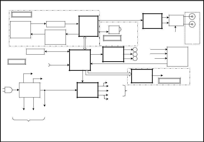
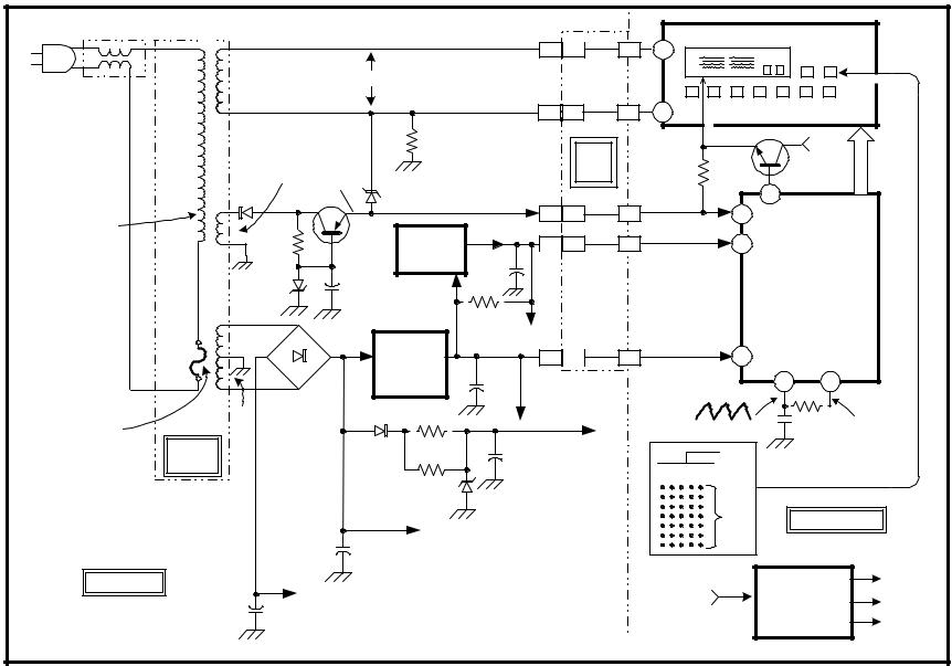
Overall Block Diagram
At the core of the 200 disc CD Changer is the System Control (Syscon) IC501. IC501 serves as the interface between the user and the mechanism. Before IC501 can respond to the user’s commands for a disc to play, it must know the following:
·If the Disc door is closed.
·If the CD Mechanism is in the chucked position.
·At which disc slot is the tray table is positioned.
Some of this information is stored in an external memory IC; the remainder IC501 will have to gather at power ON using the sensors and switches linked to the Door, Tray Table and Loading Motors.
3
Once Syscon IC501 is confident the tray table information is valid, IC501 turns the CD Changer control over to the user by accepting pushbutton commands.
The user can use the front panel controls to select another disc or play that one. When Syscon knows the loading motor is in the chucked position (loading motor switch), the CD can be played.
CD Playback
Syscon IC501 initiates CD play by sending data, clock and latch communications to IC101 on the BD board. This causes IC101 to turn on the laser, focus, tracking and spindle servos that employ the laser diode, along with the focus coil, tracking coil, sled motor and spindle motor in the optical assembly.
Information Gathering
Pressing the power ON button causes IC501 to use “IC SW” to switch on regulator IC506. IC506 apples power to the BD board, which houses the optical assembly. D+5V is also applied to the LED in the door compartment to inform the user power is ON.
After Syscon IC501 turns on power, IC501 accesses its external memory IC. Data about the disc last loaded in the CD Mechanism is returned to IC501. The disc label information is output as data to the FL Display IC for display on the front panel fluorescent tube. If there was no label information, then just the disc’s number is displayed.
Syscon now takes a series of steps to check the memory information:
Once these servos are operating, the disc information (RFO) is output. RFO is received by Servo Control IC101 which:
•Converts the data back to the original modulation scheme (EFM).
•Error corrects the data (parity error correction).
•Reconstructs its original pattern (CIRC).
•Creates additional digital samples (oversampling) to reduce noise in the final analog audio.
•Converts the signal from digital to analog form (D/A Converter).
1. Syscon activates the disc door motor to close the door if its corre- |
Analog audio is output from IC101 to the rear panel jacks. |
sponding switch indicates the door is open. |
|
2.Next, Syscon checks the loading motor switch position to see if the CD Mechanism is in the chucked position (disc loaded).
•
•
If chucked, IC501 will initiate disc PB to read its TOC.
If unchucked, IC501 will drive the tray table motor, rotating its discs
past the disc sensors. While the tray is rotating, the tray sensors inform IC501 of the disc slot location while the disc sensor tells IC501 if there is a disc present at that slot. The last disc played according to memory will be loaded and its TOC read (if present).
BD BOARD |
|
|
|
LINE OUT |
|
IC401 |
|
L |
|
|
|
|
|
IC101 |
|
MUTE |
|||
OPTICAL |
A-F |
RF AMP |
RFO |
|
|
AUDIO |
|
||
|
|
SERVO |
D |
DIGITAL |
AMP |
|
R |
||
PICK-UP |
|
|
|
CONTROL/ |
OUT |
|
|
|
|
|
|
|
OPTICAL |
|
|
AUDIO |
|||
ASSEMBLY |
COIL & |
|
DSP |
|
|
|
|||
|
|
OUTPUT |
|
RESET |
|||||
KSS213B |
|
|
|
|
|
OUTPUT |
|||
|
MOTOR |
ERROR |
|
JACK BD. |
|
||||
|
|
|
|
|
FROM |
(JACK |
|||
|
|
DRIVER |
SIGNAL |
|
|
|
|
IC506 |
BD.) |
|
MEMORY |
|
|
|
IC503 |
M |
DOOR |
|
|
|
|
|
|
MOTOR |
M |
TRAY |
SWITCH OR |
||
|
|
|
IC501 |
||||||
|
|
|
DRIVER |
M |
LOADING |
SENSOR |
|
||
MAIN BD. |
FRONT |
|
SYSTEM |
|
|||||
|
|
|
|
|
|
||||
|
CONTROL |
|
|
|
|
|
|||
|
PANEL |
|
|
|
|
|
|
||
|
|
|
|
|
|
|
|
|
|
|
BUTTONS |
|
FL DATA,CLK,LATCH |
IC701 |
FL DISPLAY |
|
|||
|
-13.5V SOURCE |
IC |
|
|
|
||||
|
|
FL DISPLAY |
TUBE |
|
|||||
|
|
+5V SOURCE |
SW |
DISC DOOR |
|
||||
|
|
DRIVER |
DISPLAY BD. |
|
|||||
|
|
|
|
|
|||||
|
|
|
|
|
LIGHT |
|
|
|
|
POWER |
|
|
IC506REG |
D+5V |
TO BD BOARD |
|
|
||
SUPPLY |
|
|
/SW |
+7V |
|
|
|||
|
|
|
|
|
|
||||
|
|
|
|
|
RESET |
|
|
|
|
|
|
+11.5V |
|
|
AUDIO |
|
|
|
|
|
|
|
|
MUTE |
|
|
|
|
|
-28V |
FILAMENT |
SOURCE |
|
|
|
|
|
|
|
|
|
|
|
|
|
|
|
||
SOURCE VOLTAGE |
|
|
|
|
|
|
|
|
|
TO DISPLAY BD. |
|
|
|
|
|
|
|
|
|
OVERALL BLOCK DIAGRAM (MODEL CDP-CX235) |
0A122 1251 7/5/00 |
4
Power Supply / Display
Overview
The power supply stage produces seven voltages when the CD Changer is plugged into AC. Some of these voltages from the main board power the FL Driver microprocessor IC701 and the FL indicator tube on the display board.
Power Supply
Power Supply Output
Output Voltage |
From |
Destination |
|
|
|
|
|
1. |
+11.5Vdc |
Bridge Rectifier |
Regulator/Sw IC506, |
|
|
D501-4 |
+5V Regulator IC504, |
|
|
|
Motor Driver IC503. |
|
|
|
|
2. |
13.5Vdc |
Bridge Rectifier |
Audio mute transistors |
|
|
D501-4 |
(Q325/e, Q327/e and |
|
|
|
Q425/e), Motor driver |
|
|
|
IC503. |
|
|
|
|
3. |
+5Vdc Source |
Regulator IC504 |
Syscon IC501 (not shown), |
|
|
|
FL Driver IC701. |
|
|
|
|
4. |
+5Vdc |
Bridge D501-4 & |
Mute transistors Q325/e, |
|
|
Zener D508 |
Q327/e and Q425/e. |
|
|
|
|
5. |
Reset +5V |
Reset IC505 |
Syscon IC501 (not shown), |
|
|
|
FL Driver IC701, |
|
|
|
LED Driver IC702 (not |
|
|
|
shown). |
|
|
|
|
6. |
3.7Vac |
Power Transformer |
Fluorescent Display Tube |
|
|
T901 |
filament |
|
|
|
|
7. |
-28V |
Q501/emitter |
Reference voltage for the |
|
|
|
Fluorescent Display |
|
|
|
|
+11.5V Source / -13.5V Source
When the CD Changer is plugged into AC, this voltage is applied to the primary winding of T901. The secondary winding that is center taped applies 20.6Vac to a four-diode bridge rectifier designated D501 to D504.
5
The positive output of the bridge rectifier is filtered by C501 to become the +11.5V source voltage.
The negative output of the bridge rectifier is filtered by C502 to become the –13.5V source voltage.
+5Volt Source
The +11.5V source voltage is reduced and regulated by IC504 to produce the +5V source voltage for the CD Changer.
+5Vdc
The +11.5V source voltage is reduced by R505 and R508 and applied to 5.1 volt zener diode D508 for shunt regulation. Shunt regulation is when a device like this variable resistance zener diode is placed in parallel with the load. The zener diode resistance varies to keep the voltage at the load reasonably stable.
This +5 volts that is output is used by the mute transistors Q325, Q327, and Q425 to control the left and right channel audio muting at power ON and OFF and when plugged and unplugged from AC.
D509 and C505 are used to insure there is sufficient voltage for the mute operation when the unit is unplugged. C505 holds the +5V for the mute transistors and diode D509 blocks this voltage from being used by the loads on the 11.5V line (D509/anode).
Reset +5V
When the +5Volt Source voltage outputs regulator IC504, IC505 creates a reset pulse using R506 and C507. Each one of these three parts has a role in creating the reset pulse. When the source voltage is input IC505, IC505 holds it output LOW for a fixed amount of time dependent upon IC505’s design. This LOW grounds out C507 at the output. When the IC505 releases ground, C507 is charged by R506 to +5V.
The reset output of IC505 is applied to the IC501 and IC701 microprocessors in this CD Changer. Generally, reset occurs when the reset input to a device is held LOW while power (Vcc) is applied.

T901 |
FL701 FL INDICATOR TUBE |
|
|
|
|
|
|
|
|
|
14 |
2 |
3 |
1 |
|
|
|
|
|
|
2Ω |
|
|
3.7VAC |
FILAMENT |
|
|
-28V |
|
|
|
|
|||
L901 |
|
|
|
|
|
|
|
|
|
|
|
|||||
|
|
|
|
|
|
|
|
|
|
|
|
|
|
|
||
NOISE |
|
|
|
|
|
|
|
VOLTAGE |
15 |
1 |
1 |
65 |
|
|
|
|
FILTER |
|
|
|
|
|
|
|
|
|
|
|
|
||||
|
|
|
|
|
|
R501 |
|
|
|
|
G16 |
|
|
|
||
CHOKE |
|
|
|
|
|
|
|
|
|
|
|
+5V |
|
|||
|
|
|
|
|
|
33k |
|
|
JOG |
|
|
N |
|
|||
|
|
|
|
|
|
|
|
|
|
|
P1-36 |
|||||
|
|
|
|
|
|
|
|
|
|
R701 |
|
|||||
|
|
41Ω |
|
|
|
|
|
|
BD. |
|
|
|
|
|||
|
|
-28V |
D507 |
|
|
|
Q701 |
|
|
G1-15 |
||||||
|
|
|
|
|
100k |
|
|
|||||||||
|
D505 |
|
|
|
|
|
|
55 |
|
|
||||||
|
-40V |
|
|
6.2V |
|
|
|
|
|
|
|
|
||||
|
P |
|
|
13 |
3 |
2 |
|
56 |
DIG 16 |
|
||||||
|
|
|
|
|
|
|
|
|
|
|||||||
55Ω |
|
|
|
|
|
|
|
-28V |
VFL |
|
|
|||||
|
R502 |
|
|
Q501 |
IC505 |
|
|
|
|
|
|
|
||||
|
|
|
|
|
5 |
11 |
7 |
|
60 |
|
|
|||||
|
|
|
|
|
|
|
|
|
|
|||||||
|
|
|
|
|
|
|
PST994D C507 + |
|
|
|
RESET |
|
IC701 |
|
||
|
|
D506 |
|
C503 |
|
R506 |
|
|
|
+5V |
|
|
|
|||
|
|
|
|
|
|
|
|
FL DRIVER |
|
|||||||
|
|
30V |
|
+ |
100 |
|
|
|
|
|
|
|
||||
|
|
|
|
|
|
|
|
|
|
MSM9202-03GS |
|
|||||
|
|
|
|
|
|
|
|
|
|
|
|
|
|
|
||
|
2Ω |
|
|
|
|
|
SYSCON |
|
|
|
|
|
|
|
|
|
|
|
|
|
IC504 |
IC501/30 |
7 |
9 |
9 |
+5V |
64 |
VCC |
|
|
|||
|
|
|
|
|
|
|
|
|||||||||
|
|
|
|
|
|
REG |
+ C506 |
2.5V p-p |
OSC0 OSC1 |
|
||||||
|
|
|
|
|
|
TA7805 |
+5V |
|
|
58 |
59 |
|
||||
|
|
|
|
|
|
|
OSC.2.48MHz |
|
||||||||
THERMAL |
|
|
D501- |
|
|
|
SOURCE |
|
|
|
|
|||||
2 |
Ω |
|
|
R505 |
|
|
|
|
|
|
||||||
D504 |
|
|
|
(B+) |
|
|
|
|
R706 5V p-p |
|||||||
FUSE |
|
|
|
|
|
C702 |
||||||||||
|
|
|
|
|
|
|
|
|
|
|
|
|||||
|
JACK |
|
|
|
|
D509 |
|
+ C505 |
|
|
|
|
SQ. WAVE |
|||
|
|
|
|
|
R508 |
|
|
|
|
G1 |
|
|||||
|
BD. |
|
|
|
|
|
+5V TO MUTE |
|
WORDS |
|
|
|
||||
|
|
|
|
|
|
|
D508 |
TRANSISTORS |
|
|
|
|
|
|||
|
|
|
|
|
|
|
Q325/E,Q327/E, |
|
|
|
|
|
|
|||
|
|
|
|
|
|
|
5.1V |
|
|
P |
|
|
|
|||
|
|
|
|
|
+11.5V |
Q425/E |
|
|
|
|
DISPLAY BD. |
|||||
|
|
|
|
|
|
|
|
|
(36) |
|
||||||
|
|
|
|
|
+11.5V SOURCE TO: IC506 |
|
|
|
||||||||
|
|
|
|
+ |
|
C501 |
|
|
|
|
|
|
||||
|
|
|
|
|
REGULATOR, |
|
|
|
|
|
|
|
|
|||
|
|
|
|
|
|
3300 |
|
|
|
GRIDS 1-15 |
|
|
|
|||
|
|
|
|
|
|
IC503 MOTOR DRIVER |
|
|
|
|
||||||
MAIN BD. |
|
|
|
|
|
|
|
IC702 |
FRONT |
|||||||
C502 |
|
|
-13.5V SOURCE TO: MUTE |
|
|
|
DATA, |
|
||||||||
|
|
|
|
|
|
|
LED DRIVER |
PANEL |
||||||||
|
1000 + |
|
TRANSISTORS Q325,Q327, |
|
|
|
CLK FROM |
|
M66310FP |
LED’s |
||||||
|
|
|
|
Q425 AND IC503 MOTOR DRIVER |
|
|
SYSCON IC501 |
|
|
|
||||||
POWER SUPPLY (CDP-CX235) |
1A122 1238 7/7/00 |
6
When the output of IC505 is LOW, these microprocessors are held in reset and are inactive (apparently dead).
3.7Vac
A low AC voltage from power transformer T901 is applied to the filament of the fluorescent indicator tube FL701.
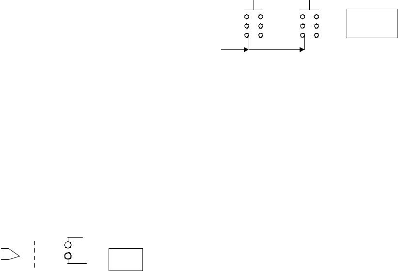
7
Grid & Plate Array
Within the FL tube there are 16 grid structures, each containing 36 plates. Each grid structure produces a character or number by luminating a combination of plates.
G1 |
G2 |
|
|
-28V
The 41-ohm secondary winding of transformer T901 produces 31.7Vac that is rectified by D505. The –40Vdc produced is regulated by Q501 using zener diode D506 for voltage stabilization.
The –28Vdc output from regulator Q501/emitter is applied to the fluorescent driver stage as the negative supply voltage and to one end of the filament via D507as the tube’s electron source.
Fluorescent Display
The FL701 Fluorescent Display tube needs the following to light a segment or a word in the tube:
•Filament voltage
•Positive voltage simultaneously applied to the grid and plate.
Basic Operation
The filament voltage comes from the power transformer T901 and the positive pulses come from FL Driver IC701.
Just like a vacuum tube, the fluorescent display tube needs a source of electrons. The electrons come from the filament, which is connected to the –28V source. A controlling grid in the middle acts as a gate to determine if electrons should pass onto the plate to make it glow. At the gate, a more positive voltage than the filament attracts the electrons and opens the gate. A grid voltage that is the same as the filament will keep electrons from leaving the filament so there is no glow.
The plate structures will be phosphorescent when struck by electrons. To get the electrons to the plate, the plate must have a positive voltage to be
attractive. |
|
P1 |
|
|
|
|
Simple FL |
|
|
P2 |
Tube |
|
|
Structure |
|
Filament |
Grid |
Plates |
|
P1 |
P4 |
P1 |
P4 |
Plate and Grid |
P2 |
P5 |
P2 |
P5 |
Structures |
P3 |
P6 |
P3 |
P6 |
|
P3
To make a specific plate glow, a grid structure is selected and a positive voltage is applied to it. At that time, the plate structures that must glow are also brought positive. In the diagram above, when G1 and P3 lines are brought HIGH, the P3 plate in the G1 structure will glow. Even though the P3 structure in the G2 structure is connected in parallel, receiving the same voltage, it will not glow because the G2 voltage is LOW at this time. The job of FL Driver IC701 is to create and time the grid and plate pulses.
Fluorescent Driver IC701
When the CD Changer is plugged into AC, Vcc is applied to IC701/pin 64, starting its internal oscillator. The R-C parts that set the frequency of this 2.48MHz oscillator (16MHz is on the schematic) are located at IC701/ pins 58 and 59.
Also at AC plug in, the FL Driver IC701 is momentarily reset. IC505 momentarily holds its output LOW when +5V is input. This LOW resets FL Driver IC701 when Vcc (power) is present at pin 64. The LOW lasts for 0.2ms (IC505) + 0.8ms (C507) = 10ms.

T901 |
FL701 FL INDICATOR TUBE |
|
|
|
|
|
|
|
|
|
14 |
2 |
3 |
1 |
|
|
|
|
|
|
2Ω |
|
|
3.7VAC |
FILAMENT |
|
|
-28V |
|
|
|
|
|||
L901 |
|
|
|
|
|
|
|
|
|
|
|
|||||
|
|
|
|
|
|
|
|
|
|
|
|
|
|
|
||
NOISE |
|
|
|
|
|
|
|
VOLTAGE |
15 |
1 |
1 |
65 |
|
|
|
|
FILTER |
|
|
|
|
|
|
|
|
|
|
|
|
||||
|
|
|
|
|
|
R501 |
|
|
|
|
G16 |
|
|
|
||
CHOKE |
|
|
|
|
|
|
|
|
|
|
|
+5V |
|
|||
|
|
|
|
|
|
33k |
|
|
JOG |
|
|
N |
|
|||
|
|
|
|
|
|
|
|
|
|
|
P1-36 |
|||||
|
|
|
|
|
|
|
|
|
|
R701 |
|
|||||
|
|
41Ω |
|
|
|
|
|
|
BD. |
|
|
|
|
|||
|
|
-28V |
D507 |
|
|
|
Q701 |
|
|
G1-15 |
||||||
|
|
|
|
|
100k |
|
|
|||||||||
|
D505 |
|
|
|
|
|
|
55 |
|
|
||||||
|
-40V |
|
|
6.2V |
|
|
|
|
|
|
|
|
||||
|
P |
|
|
13 |
3 |
2 |
|
56 |
DIG 16 |
|
||||||
|
|
|
|
|
|
|
|
|
|
|||||||
55Ω |
|
|
|
|
|
|
|
-28V |
VFL |
|
|
|||||
|
R502 |
|
|
Q501 |
IC505 |
|
|
|
|
|
|
|
||||
|
|
|
|
|
5 |
11 |
7 |
|
60 |
|
|
|||||
|
|
|
|
|
|
|
|
|
|
|||||||
|
|
|
|
|
|
|
PST994D C507 + |
|
|
|
RESET |
|
IC701 |
|
||
|
|
D506 |
|
C503 |
|
R506 |
|
|
|
+5V |
|
|
|
|||
|
|
|
|
|
|
|
|
FL DRIVER |
|
|||||||
|
|
30V |
|
+ |
100 |
|
|
|
|
|
|
|
||||
|
|
|
|
|
|
|
|
|
|
MSM9202-03GS |
|
|||||
|
|
|
|
|
|
|
|
|
|
|
|
|
|
|
||
|
2Ω |
|
|
|
|
|
SYSCON |
|
|
|
|
|
|
|
|
|
|
|
|
|
IC504 |
IC501/30 |
7 |
9 |
9 |
+5V |
64 |
VCC |
|
|
|||
|
|
|
|
|
|
|
|
|||||||||
|
|
|
|
|
|
REG |
+ C506 |
2.5V p-p |
OSC0 OSC1 |
|
||||||
|
|
|
|
|
|
TA7805 |
+5V |
|
|
58 |
59 |
|
||||
|
|
|
|
|
|
|
OSC.2.48MHz |
|
||||||||
THERMAL |
|
|
D501- |
|
|
|
SOURCE |
|
|
|
|
|||||
2 |
Ω |
|
|
R505 |
|
|
|
|
|
|
||||||
D504 |
|
|
|
(B+) |
|
|
|
|
R706 5V p-p |
|||||||
FUSE |
|
|
|
|
|
C702 |
||||||||||
|
|
|
|
|
|
|
|
|
|
|
|
|||||
|
JACK |
|
|
|
|
D509 |
|
+ C505 |
|
|
|
|
SQ. WAVE |
|||
|
|
|
|
|
R508 |
|
|
|
|
G1 |
|
|||||
|
BD. |
|
|
|
|
|
+5V TO MUTE |
|
WORDS |
|
|
|
||||
|
|
|
|
|
|
|
D508 |
TRANSISTORS |
|
|
|
|
|
|||
|
|
|
|
|
|
|
Q325/E,Q327/E, |
|
|
|
|
|
|
|||
|
|
|
|
|
|
|
5.1V |
|
|
P |
|
|
|
|||
|
|
|
|
|
+11.5V |
Q425/E |
|
|
|
|
DISPLAY BD. |
|||||
|
|
|
|
|
|
|
|
|
(36) |
|
||||||
|
|
|
|
|
+11.5V SOURCE TO: IC506 |
|
|
|
||||||||
|
|
|
|
+ |
|
C501 |
|
|
|
|
|
|
||||
|
|
|
|
|
REGULATOR, |
|
|
|
|
|
|
|
|
|||
|
|
|
|
|
|
3300 |
|
|
|
GRIDS 1-15 |
|
|
|
|||
|
|
|
|
|
|
IC503 MOTOR DRIVER |
|
|
|
|
||||||
MAIN BD. |
|
|
|
|
|
|
|
IC702 |
FRONT |
|||||||
C502 |
|
|
-13.5V SOURCE TO: MUTE |
|
|
|
DATA, |
|
||||||||
|
|
|
|
|
|
|
LED DRIVER |
PANEL |
||||||||
|
1000 + |
|
TRANSISTORS Q325,Q327, |
|
|
|
CLK FROM |
|
M66310FP |
LED’s |
||||||
|
|
|
|
Q425 AND IC503 MOTOR DRIVER |
|
|
SYSCON IC501 |
|
|
|
||||||
POWER SUPPLY (CDP-CX235) |
1A122 1238 7/7/00 |
8
Plug into AC |
|
|
+5V |
T |
|
1 |
Reset |
|
|
2 |
10msec/div |
C H 1 5 .00 V = |
|
C H 2!5 .00 V= |
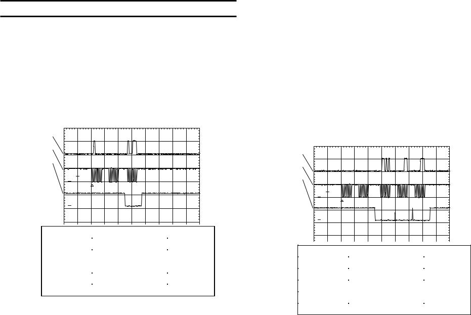
M T B 10.0m s- 3.16dv ch1+ |
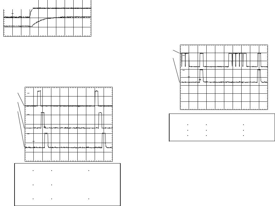
After reset, IC701 begins normal operation, producing sequential grid pulses first. When IC701/pin 60 goes HIGH (+5V), IC701 outputs a positive going pulse at each grid pin, one after the other. Each grid pulse is applied to a grid cluster consisting of 36 individual plate structures. After all 16 grids are pulsed (G1 – G16), the sequence repeats. Nothing appears in the display at plug-in because the fluorescent tube has not received plate voltage.
The waveform below shows grid pulses applied to G14, G15, and G16 of the fluorescent tube.
9
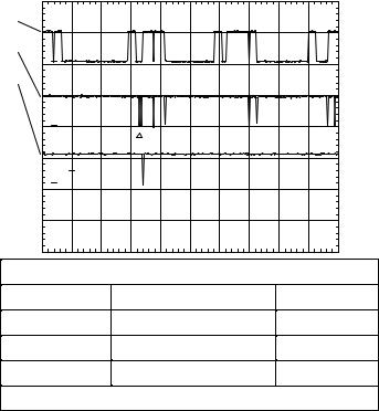
Plate voltage pulses appear only when the CD Changer is powered ON. At power ON, Syscon (IC501 is not shown) sends data to IC701 so it can output these pulses. Positive pulses are output the appropriate plate pins P1-36 to form a number, letter or word when a grid pulse is simultaneously present.
The following waveforms show a plate signal (Ch 1) compared to the grid 16 signal (Ch 3). This plate segment is lit at the grid assembly 16 location when both the plate and the grid outputs are HIGH.
ch1
1
ch3
3
T
ch1
ch2
ch3
ch2:dc = - 27 . 3 V, rms = 28 . 3 V
1
pkpk= 33.8 V, freq= 304 Hz
2
3
T
C H 1 2 0 . 0 V =
C H 2 2 0 . 0 V =
C H 3 ! 2 0 . 0 V = C H P M T B 5 0 0 u s - 2 . 3 4 d v c h 3 +
Fluorescent tube Grid pulses at Power OFF
Chan |
Name |
Location |
Voltage |
|
|
|
|
1 |
G14 |
IC701/pin 53 |
30Vp-p |
|
|
|
|
2 |
G15 |
IC701/pin 54 |
30Vp-p |
|
|
|
|
3 |
G16 |
IC701/pin 55 |
30Vp-p |
|
|
|
|
Time base = 500usec
CH1 20.0 V=
CH3!20.0 V= CHP MTB 500us- 2.34dv ch3+
Fluorescent tube pulses during Power ON
Chan |
Name |
Location |
Voltage |
1 |
P14 |
IC701/pin 18 |
30Vp-p |
3 |
G16 |
IC701/pin 55 |
30Vp-p |
Time base = 500usec
By looking at Channel 1, we see that the plate signal also goes high at times when grid 16 is not HIGH (Ch 3 = LOW). This means a similar plate at a different grid is lit at this time.
T901 |
FL701 FL INDICATOR TUBE |
|
|
|
|
|
|
|
|
|
14 |
2 |
3 |
1 |
|
|
|
|
|
|
2Ω |
|
|
3.7VAC |
FILAMENT |
|
|
-28V |
|
|
|
|
|||
L901 |
|
|
|
|
|
|
|
|
|
|
|
|||||
|
|
|
|
|
|
|
|
|
|
|
|
|
|
|
||
NOISE |
|
|
|
|
|
|
|
VOLTAGE |
15 |
1 |
1 |
65 |
|
|
|
|
FILTER |
|
|
|
|
|
|
|
|
|
|
|
|
||||
|
|
|
|
|
|
R501 |
|
|
|
|
G16 |
|
|
|
||
CHOKE |
|
|
|
|
|
|
|
|
|
|
|
+5V |
|
|||
|
|
|
|
|
|
33k |
|
|
JOG |
|
|
N |
|
|||
|
|
|
|
|
|
|
|
|
|
|
P1-36 |
|||||
|
|
|
|
|
|
|
|
|
|
R701 |
|
|||||
|
|
41Ω |
|
|
|
|
|
|
BD. |
|
|
|
|
|||
|
|
-28V |
D507 |
|
|
|
Q701 |
|
|
G1-15 |
||||||
|
|
|
|
|
100k |
|
|
|||||||||
|
D505 |
|
|
|
|
|
|
55 |
|
|
||||||
|
-40V |
|
|
6.2V |
|
|
|
|
|
|
|
|
||||
|
P |
|
|
13 |
3 |
2 |
|
56 |
DIG 16 |
|
||||||
|
|
|
|
|
|
|
|
|
|
|||||||
55Ω |
|
|
|
|
|
|
|
-28V |
VFL |
|
|
|||||
|
R502 |
|
|
Q501 |
IC505 |
|
|
|
|
|
|
|
||||
|
|
|
|
|
5 |
11 |
7 |
|
60 |
|
|
|||||
|
|
|
|
|
|
|
|
|
|
|||||||
|
|
|
|
|
|
|
PST994D C507 + |
|
|
|
RESET |
|
IC701 |
|
||
|
|
D506 |
|
C503 |
|
R506 |
|
|
|
+5V |
|
|
|
|||
|
|
|
|
|
|
|
|
FL DRIVER |
|
|||||||
|
|
30V |
|
+ |
100 |
|
|
|
|
|
|
|
||||
|
|
|
|
|
|
|
|
|
|
MSM9202-03GS |
|
|||||
|
|
|
|
|
|
|
|
|
|
|
|
|
|
|
||
|
2Ω |
|
|
|
|
|
SYSCON |
|
|
|
|
|
|
|
|
|
|
|
|
|
IC504 |
IC501/30 |
7 |
9 |
9 |
+5V |
64 |
VCC |
|
|
|||
|
|
|
|
|
|
|
|
|||||||||
|
|
|
|
|
|
REG |
+ C506 |
2.5V p-p |
OSC0 OSC1 |
|
||||||
|
|
|
|
|
|
TA7805 |
+5V |
|
|
58 |
59 |
|
||||
|
|
|
|
|
|
|
OSC.2.48MHz |
|
||||||||
THERMAL |
|
|
D501- |
|
|
|
SOURCE |
|
|
|
|
|||||
2 |
Ω |
|
|
R505 |
|
|
|
|
|
|
||||||
D504 |
|
|
|
(B+) |
|
|
|
|
R706 5V p-p |
|||||||
FUSE |
|
|
|
|
|
C702 |
||||||||||
|
|
|
|
|
|
|
|
|
|
|
|
|||||
|
JACK |
|
|
|
|
D509 |
|
+ C505 |
|
|
|
|
SQ. WAVE |
|||
|
|
|
|
|
R508 |
|
|
|
|
G1 |
|
|||||
|
BD. |
|
|
|
|
|
+5V TO MUTE |
|
WORDS |
|
|
|
||||
|
|
|
|
|
|
|
D508 |
TRANSISTORS |
|
|
|
|
|
|||
|
|
|
|
|
|
|
Q325/E,Q327/E, |
|
|
|
|
|
|
|||
|
|
|
|
|
|
|
5.1V |
|
|
P |
|
|
|
|||
|
|
|
|
|
+11.5V |
Q425/E |
|
|
|
|
DISPLAY BD. |
|||||
|
|
|
|
|
|
|
|
|
(36) |
|
||||||
|
|
|
|
|
+11.5V SOURCE TO: IC506 |
|
|
|
||||||||
|
|
|
|
+ |
|
C501 |
|
|
|
|
|
|
||||
|
|
|
|
|
REGULATOR, |
|
|
|
|
|
|
|
|
|||
|
|
|
|
|
|
3300 |
|
|
|
GRIDS 1-15 |
|
|
|
|||
|
|
|
|
|
|
IC503 MOTOR DRIVER |
|
|
|
|
||||||
MAIN BD. |
|
|
|
|
|
|
|
IC702 |
FRONT |
|||||||
C502 |
|
|
-13.5V SOURCE TO: MUTE |
|
|
|
DATA, |
|
||||||||
|
|
|
|
|
|
|
LED DRIVER |
PANEL |
||||||||
|
1000 + |
|
TRANSISTORS Q325,Q327, |
|
|
|
CLK FROM |
|
M66310FP |
LED’s |
||||||
|
|
|
|
Q425 AND IC503 MOTOR DRIVER |
|
|
SYSCON IC501 |
|
|
|
||||||
POWER SUPPLY (CDP-CX235) |
1A122 1238 7/7/00 |
10
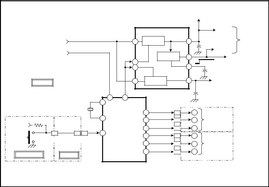
Power On
Once the CD Changer is plugged into AC, pressing the front panel Power button permits Syscon to enable regulator IC506. IC506 outputs D+5V, +7V, and a reset signal to power the remaining devices on the BD board and turn on 2 LEDs to illuminate the disc door compartment.
AC Power Only
When the CD changer was plugged into AC, Syscon IC501 received power at pin 37 and was fully functional as marked by the X501 activity at pins 31 and 32. There is even data and clock signals leaving IC501/pins 18, 19 and 58. These signals go to FL Display Driver IC701, but there is no instruction to turn on the front panel display while the unit is still OFF.
P M 3 3 9 4 , F L U K E & P H I L I P S
ch1
ch2
1
ch3
T
2
3
C H 1 5 . 0 0 V =
IC501 Activity at Power OFF
Channel |
|
Name |
CN501/pin |
|
|
|
|
1. |
FL Data |
1 |
|
|
|
|
|
2. |
FL |
CLK (Clock) |
2 |
|
|
|
|
3. |
FL |
LT (Latch) |
4 |
|
|
|
|
Time base = 50usec/div
Power ON
Syscon IC501 receives the power ON command from the front panel push button at pin 44 (LOW). IC501 responds by outputting a HIGH at IC SW
11
pin 65 to enable regulator IC506. IC506 has three outputs: 1. D+5V from pin 2 is used to:
•Power the digital ICs on the DB board; and
•Turn on the LED at the disc door compartment. This also lets the user know the unit is ON.
2. +7V from pin 9 is used to:
•Power the focus/sled/tracking driver IC102; and
•Power the coils and motors on the BD board
3. XRST from pin 6 goes HIGH to:
•Unmute the analog audio output lines; and
•Enable Servo Control IC101 and the focus/sled/tracking driver IC102 on the BD board.
Communications IC501 – IC701
At power On, the communications activity increases between IC501 and IC701. This is to provide constant update information to the display IC701.
ch1
ch2
1
ch3
T
2
3
C H 1 5 . 0 0 V =
C H 2 ! 5 0 0 V =
IC501 Activity at Power ON
Channel |
|
Name |
CN501/pin |
|
|
|
|
1. |
FL Data |
1 |
|
|
|
|
|
2. |
FL |
CLK (Clock) |
2 |
|
|
|
|
3. |
FL |
LT (Latch) |
4 |
|
|
|
|
Time base = 50usec/div

|
|
|
|
|
|
|
|
|
|
|
DOOR |
|
|
|
|
|
|
|
|
|
|
|
|
|
|
|
|
LUMINATION |
|
D+5V |
|
||
|
|
|
|
|
|
|
|
|
|
IC506 LA5616 |
|
|
|
|||
|
|
|
|
|
|
|
|
|
|
|
|
SOURCE |
TO |
|||
|
|
|
|
|
|
|
VCC |
|
|
|
|
|
|
|
|
|
|
|
+11.5V |
|
|
|
|
1 |
|
REG |
|
2 |
C509 |
XRST TO |
BD. |
||
|
|
|
|
|
|
|
|
|
|
|
|
|
IC101/3, |
BOARD |
||
|
|
+5V |
|
|
|
|
|
|
|
|
|
|
|
IC102/15 |
|
|
|
|
|
|
|
|
|
|
|
RESET |
6 |
|
|
POWER ON |
|||
|
|
|
|
|
|
|
|
EN1 |
|
|
||||||
|
|
|
|
|
|
|
|
|
|
|
|
|
MUTE |
|
||
|
|
|
|
|
|
|
|
4 |
|
|
|
|
+5V |
|
|
|
|
|
|
|
|
|
|
|
8 |
|
|
|
7 |
|
(MAIN BD.) |
||
|
|
|
|
|
|
|
|
|
|
|
|
|
||||
|
|
|
|
|
|
|
|
|
EN2 |
|
4.8V |
C511 |
Q325,Q327, |
|||
|
|
|
|
|
|
|
|
|
|
|
||||||
|
|
|
|
|
|
|
|
|
|
|
|
|
Q425 |
|
||
|
|
|
|
|
|
|
|
10 |
|
REG |
|
9 |
|
+7V |
|
|
|
MAIN BD. |
|
|
|
|
VCC |
|
|
|
|
|
|||||
|
|
|
|
|
|
|
|
|
|
|
SOURCE TO |
|
||||
|
|
|
|
|
|
|
|
|
|
|
|
|
|
|||
|
|
|
|
|
VCC |
+5V ICSW |
|
|
|
+ |
|
DRIVER |
|
|||
|
|
|
|
|
|
|
|
C508 |
|
IC102 (B BD.) |
|
|||||
|
|
|
|
50mVp-p |
|
37 |
65 |
|
|
CN501 |
|
|
||||
|
|
|
|
|
|
|
|
|
|
|
||||||
|
|
|
|
32 |
|
|
|
|
|
|
|
|
||||
|
|
|
|
|
|
|
|
|
|
|
IC701/PIN |
|
|
|
||
|
|
|
X501 |
|
|
|
|
|
|
|
|
|
|
|||
|
|
|
|
|
|
|
|
FL DATA |
|
|
|
|
|
|
||
|
|
|
10MHz |
|
|
|
|
18 |
1 |
63 |
IC701 |
|
|
|||
|
|
|
|
|
|
|
|
|
|
|||||||
|
|
|
|
|
31 |
|
|
|
|
FL CLK |
|
|
|
|
||
PUSH |
R732 |
|
4Vp-p |
|
|
|
19 |
2 |
62 |
FL DRIVER |
|
|
||||
|
|
|
IC501 |
|
|
|
|
|||||||||
BUTTONS |
|
|
|
KEY 1 |
|
|
58 |
FL LT |
4 |
61 |
(DISPLAY BD.) |
|
||||
|
|
|
|
SYSCON |
|
|
|
|
|
|||||||
|
|
|
|
|
|
|
|
|
|
|
||||||
POWER |
|
2 |
7 |
9 |
44 |
CXP84340-075Q |
50 |
DATA |
18 |
5 |
|
|
|
|
||
|
CN701/602 |
CN601/501 |
|
IC101 |
|
|
||||||||||
|
|
|
|
|
|
CLK |
|
|
|
|
||||||
|
|
|
|
|
|
|
|
|
48 |
20 |
7 |
DSP |
|
|
|
|
|
|
|
|
|
|
|
|
|
|
|
|
|
||||
|
|
|
|
|
|
|
|
|
49 |
XLT |
19 |
6 |
(BD.BD.) |
|
|
|
|
|
|
|
|
|
|
|
|
|
|
|
|
||||
DISPLAY BD. |
JOG BD. |
|
|
|
|
|
|
|
|
|
|
|||||
|
|
|
|
|
|
CN502 |
IC101/PIN |
|
|
|
||||||
|
|
|
|
|
|
|
|
|
|
|
|
|
||||
POWER ON
2A122 1242 |
6 28 2000 |
12
13
Communications IC501 – IC101
Communications from Syscon to Servo Control IC101 does not occur until the disc is chucked on the spindle motor and ready to play (after the
loading motor finishes chucking the disc). This communications is shown |
|||
below: |
, |
|
|
|
ch1 |
|
|
|
ch2 |
|
|
|
1 |
|
|
|
ch3 |
|
|
|
2 |
|
|
|
T |
|
|
|
3 |
|
|
|
C H 1 5 . 0 0 V = |
|
|
|
C H 2 ! 5 . 0 0 V = |
|
|
|
C H 3 ! 5 . 0 0 V = C H P M T B 1 . 0 0 m s - 3 . 2 4 d v c h 3 - |
|
|
|
|
IC501 Activity at CD Play |
|
|
Channel |
Name |
CN502/pin |
|
1. |
Data |
18 |
|
2. |
CLK (Clock) |
20 |
|
3. |
XLT (Latch) |
19 |
Time base = 1msec/div
|
|
|
|
|
|
|
|
|
|
|
DOOR |
|
|
|
|
|
|
|
|
|
|
|
|
|
|
|
|
LUMINATION |
|
D+5V |
|
||
|
|
|
|
|
|
|
|
|
|
IC506 LA5616 |
|
|
|
|||
|
|
|
|
|
|
|
|
|
|
|
|
SOURCE |
TO |
|||
|
|
|
|
|
|
|
VCC |
|
|
|
|
|
|
|
|
|
|
|
+11.5V |
|
|
|
|
1 |
|
REG |
|
2 |
C509 |
XRST TO |
BD. |
||
|
|
|
|
|
|
|
|
|
|
|
|
|
IC101/3, |
BOARD |
||
|
|
+5V |
|
|
|
|
|
|
|
|
|
|
|
IC102/15 |
|
|
|
|
|
|
|
|
|
|
|
RESET |
6 |
|
|
POWER ON |
|||
|
|
|
|
|
|
|
|
EN1 |
|
|
||||||
|
|
|
|
|
|
|
|
|
|
|
|
|
MUTE |
|
||
|
|
|
|
|
|
|
|
4 |
|
|
|
|
+5V |
|
|
|
|
|
|
|
|
|
|
|
8 |
|
|
|
7 |
|
(MAIN BD.) |
||
|
|
|
|
|
|
|
|
|
|
|
|
|
||||
|
|
|
|
|
|
|
|
|
EN2 |
|
4.8V |
C511 |
Q325,Q327, |
|||
|
|
|
|
|
|
|
|
|
|
|
||||||
|
|
|
|
|
|
|
|
|
|
|
|
|
Q425 |
|
||
|
|
|
|
|
|
|
|
10 |
|
REG |
|
9 |
|
+7V |
|
|
|
MAIN BD. |
|
|
|
|
VCC |
|
|
|
|
|
|||||
|
|
|
|
|
|
|
|
|
|
|
SOURCE TO |
|
||||
|
|
|
|
|
|
|
|
|
|
|
|
|
|
|||
|
|
|
|
|
VCC |
+5V ICSW |
|
|
|
+ |
|
DRIVER |
|
|||
|
|
|
|
|
|
|
|
C508 |
|
IC102 (B BD.) |
|
|||||
|
|
|
|
50mVp-p |
|
37 |
65 |
|
|
CN501 |
|
|
||||
|
|
|
|
|
|
|
|
|
|
|
||||||
|
|
|
|
32 |
|
|
|
|
|
|
|
|
||||
|
|
|
|
|
|
|
|
|
|
|
IC701/PIN |
|
|
|
||
|
|
|
X501 |
|
|
|
|
|
|
|
|
|
|
|||
|
|
|
|
|
|
|
|
FL DATA |
|
|
|
|
|
|
||
|
|
|
10MHz |
|
|
|
|
18 |
1 |
63 |
IC701 |
|
|
|||
|
|
|
|
|
|
|
|
|
|
|||||||
|
|
|
|
|
31 |
|
|
|
|
FL CLK |
|
|
|
|
||
PUSH |
R732 |
|
4Vp-p |
|
|
|
19 |
2 |
62 |
FL DRIVER |
|
|
||||
|
|
|
IC501 |
|
|
|
|
|||||||||
BUTTONS |
|
|
|
KEY 1 |
|
|
58 |
FL LT |
4 |
61 |
(DISPLAY BD.) |
|
||||
|
|
|
|
SYSCON |
|
|
|
|
|
|||||||
|
|
|
|
|
|
|
|
|
|
|
||||||
POWER |
|
2 |
7 |
9 |
44 |
CXP84340-075Q |
50 |
DATA |
18 |
5 |
|
|
|
|
||
|
CN701/602 |
CN601/501 |
|
IC101 |
|
|
||||||||||
|
|
|
|
|
|
CLK |
|
|
|
|
||||||
|
|
|
|
|
|
|
|
|
48 |
20 |
7 |
DSP |
|
|
|
|
|
|
|
|
|
|
|
|
|
|
|
|
|
||||
|
|
|
|
|
|
|
|
|
49 |
XLT |
19 |
6 |
(BD.BD.) |
|
|
|
|
|
|
|
|
|
|
|
|
|
|
|
|
||||
DISPLAY BD. |
JOG BD. |
|
|
|
|
|
|
|
|
|
|
|||||
|
|
|
|
|
|
CN502 |
IC101/PIN |
|
|
|
||||||
|
|
|
|
|
|
|
|
|
|
|
|
|
||||
POWER ON
2A122 1242 |
6 28 2000 |
14
15
Door Motor Drive
The sliding door in the model CDP-CX235 was an improved feature over the previous manual trap door that the user pulled down to access the disc tray table. The sliding door mechanism consists of a motor that drives a series of gears to slide the door on plastic tracks. The door motor stops turning when the limit switch is toggled in the closed or open position.
Drive
Syscon IC501 applies an output voltage to pin 23 or pin 24 to drive the motor. The resultant positive or negative voltage is applied to the door motor.
Door Motor Drive
Movement |
IC501/pin 24 |
IC501/pin 23 |
IC503/pin 9 |
Door Opening |
4.7V |
0V |
-3.6V |
Door Closing |
0V |
4.8V |
+3.7V |
Operation
Syscon IC501 controls the door movement. Only after the CD Changer is powered ON will IC501 respond to the OPEN/CLOSE Door button at the Key 2 input (IC501/pin 43).
Pressing the door button causes IC501 to check the position of the door. S810, a 3-position switch, places one of three voltages at Syscon IC501/ pin 39 to indicate the door position.
Door Position Feedback
Door Position |
Location |
Voltage |
Closed |
CN504/pin 1 |
2.5V |
Neutral (in-between) |
CN504/pin 1 |
5V |
Open |
CN504/pin 1 |
0V |
A closed door will be driven open and vice versa.
Feedback
As the door moves, S810 enters the neutral position and 5V is applied to IC501/pin 39. When the door reaches the end of travel the door toggles the S810 limit switch to the other end. IC501/pin 39 is lowered to either 2.5 or 0V. IC501 responds by stopping the motor voltage at pin 23 or 24
R620
+5V
CN601/501
6 10
S621 
 4
4  12
12
OPEN/  CLOSE JOG DOOR BD.
+5V |
|
|
|
|
|
C551 |
|
|
|
|
|
|
R553 |
+11.5V |
|
|
|
|
|
|
|
|
|
|
||
|
|
|
|
|
R557 |
|
|
|
|
|
|
|
|
(VCC) |
|
|
|
72 |
73 |
|
|
|
12 |
|
|
|
|
DR |
|
R552 |
- |
|
|
|
|
IC501 |
OUT |
24 |
8 |
|
|
D OUT |
|
|
|
|
|
|
|
|
|||
SYSCON |
|
|
+ |
9 |
OUT 3 |
3 |
|
|
CXP84340 DR 23 |
7 |
IC503 |
R558 |
DOOR |
||||
|
IN |
|
R551 |
CXA1291P 1/3 |
|
|||
|
DOOR |
|
|
|
MOTOR BD. |
|||
|
|
|
13 14 |
|
|
|||
KEY 2 |
|
|
C552 |
|
|
|||
SW. |
|
|
-13.5V |
|
|
|
||
43 |
39 |
|
|
(-VCC) |
|
|
D IN |
|
|
|
|
|
|
|
|
M |
|
|
|
|
|
R554 |
|
|
4 |
|
|
|
|
|
R555 |
R556 |
M810 |
||
|
|
|
|
|
1.2 Ω |
1.2Ω |
||
|
|
|
|
|
|
|||
|
|
|
|
|
|
|
2 |
|
C620 |
|
|
|
|
|
|
GND |
|
|
|
|
|
|
|
|
|
|
|
|
|
|
|
DR-SW. |
1 |
|
|
|
R543 |
|
CN504/811 |
|
||||
|
|
|
|
|
||||
|
|
|
|
1 |
2 |
|||
|
|
|
|
|
|
|
||
|
|
|
|
|
|
|
CN812/810 |
|
+5V |
|
OPEN |
|
|
|
|
R807 |
NEUTRAL |
|
|
|
|
|
CLOSE |
|
DOOR |
S810 |
|
|
|
|
SW BD. |
|
DOOR MOTOR DRIVE |
3A122 1243 6 28 2000 |
16
 Loading...