


PD-10-K
ORDER NO.
PIONEER CORPORATION 1-1, Shin-ogura, Saiwai-ku, Kawasaki-shi, Kanagawa 212-0031, Japan
PIONEER ELECTRONICS (USA) INC. P.O. Box 1760, Long Beach, CA 90801-1760, U.S.A.
PIONEER EUROPE NV Haven 1087, Keetberglaan 1, 9120 Melsele, Belgium
PIONEER ELECTRONICS ASIACENTRE PTE. LTD. 253 Alexandra Road, #04-01, Singapore 159936
PIONEER CORPORATION
2012
2012 Printed in Japan
PD-30-K
RRV4333
Super Audio CD Player
PD-30-K
PD-30-S
PD-10-K
PD-10-S
PD-10
THIS MANUAL IS APPLICABLE TO THE FOLLOWING MODEL(S) AND TYPE(S).
Model Type Power Requirement Remarks
PD-30-K, PD-30-S PWSYXZT8 AC 220 V to 230 V
PD-10-K, PD-10-S PWSYXZT8 AC 220 V to 230 V
PD-10 FXZT AC 110 V
K-MZV JULY
2
PD-30-K
1
2 3 4
A
B
C
D
E
F
1
2 3 4
SAFETY INFORMATION
LABEL CHECK
WARNING
This product may contain a chemical known to the State of California to cause cancer, or birth defects or other reproductive
harm.
Health & Safety Code Section 25249.6 - Proposition 65
This service manual is intended for qualified service technicians; it is not meant for the casual do-it-
yourselfer. Qualified technicians have the necessary test equipment and tools, and have been trained
to properly and safely repair complex products such as those covered by this manual.
Improperly performed repairs can adversely affect the safety and reliability of the product and may
void the warranty. If you are not qualified to perform the repair of this product properly and safely, you
should not risk trying to do so and refer the repair to a qualified service technician.
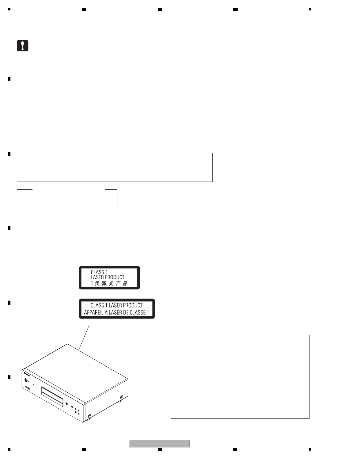
WARNING !
THE AEL (ACCESSIBLE EMISSION LEVEL) OF THE LASER POWER OUTPUT IS LESS THAN CLASS 1
BUT THE LASER COMPONENT IS CAPABLE OF EMITTING RADIATION EXCEEDING THE LIMIT FOR
CLASS 1.
A SPECIALLY INSTRUCTED PERSON SHOULD DO SERVICING OPERATION OF THE APPARATUS.
LASER DIODE CHARACTERISTICS
FOR CD : MAXIMUM OUTPUT POWER : 5 mW
WAVELENGTH : 780 nm
Additional Laser Caution
1.
• Laser diode is driving with Q2309, Q2310 (650 nm LD) and Q2308,
Q2311 (780 nm LD) on the MAIN PCB Assy.
Therefore, when short-circuit between the emitter and collector of these
transistors or the base voltage is supplied for transistors turn on, the
laser oscillates. (failure mode)
• In the test mode ∗, there is the mode that the laser oscillates except
for the disc judgment and playback. LD ON mode in the test mode
oscillates with the laser forcibly.
2. When the cover is open, close viewing through the objective lens with
the naked eye will cause exposure to the laser beam.
(Printed on the Rear Panel)
PWSYXZT8 model
FXZT model
∗: See page 28.

3
PD-30-K
5
6 7 8
5
6 7 8
A
B
C
D
E
F
CONTENTS
SAFETY INFORMATION.......................................................................................................................................................... 2
1. SERVICE PRECAUTIONS ....................................................................................................................................................4
1.1 NOTES ON SOLDERING...............................................................................................................................................4
1.2 WHEN REPLACING MECHA ASSY...............................................................................................................................4
2. SPECIFICATIONS ................................................................................................................................................................. 5
3. BASIC ITEMS FOR SERVICE .............................................................................................................................................. 6
3.1 CHECK POINTS AFTER SERVICING ........................................................................................................................... 6
3.2 JIGS LIST ....................................................................................................................................................................... 6
3.3 PCB LOCATIONS ...........................................................................................................................................................7
4. BLOCK DIAGRAM ................................................................................................................................................................8
4.1 OVERALL WIRING DIAGRAM ....................................................................................................................................... 8
4.2 OVERALL BLOCK DIAGRAM....................................................................................................................................... 10
4.3 POWER BLOCK DIAGRAM ......................................................................................................................................... 12
5. DIAGNOSIS ........................................................................................................................................................................ 13
5.1 TROUBLESHOOTING..................................................................................................................................................13
5.2 METHOD FOR DIAGNOSING DEGRADATION OF THE LDS ON THE PICKUP ASSY .............................................15
5.3 IC INFORMATION ........................................................................................................................................................ 16
6. SERVICE MODE................................................................................................................................................................. 28
6.1 TEST MODE.................................................................................................................................................................28
7. DISASSEMBLY ................................................................................................................................................................... 30
8. EACH SETTING AND ADJUSTMENT................................................................................................................................34
8.1 HOW TO UPDATE THE FIRMWARE............................................................................................................................34
8.2 DEFAULT SETTING...................................................................................................................................................... 34
9. EXPLODED VIEWS AND PARTS LIST............................................................................................................................... 36
9.1 PACKING SECTION .....................................................................................................................................................36
9.2 EXTERIOR SECTION .................................................................................................................................................. 38
10. SCHEMATIC DIAGRAM .................................................................................................................................................... 42
10.1 MAIN PCB ASSY (1/8) ...............................................................................................................................................42
10.2 MAIN PCB ASSY (2/8) ...............................................................................................................................................44
10.3 M
AIN PCB ASSY (3/8) ...............................................................................................................................................46
10.4 MAIN PCB ASSY (4/8) ...............................................................................................................................................48
10.5 MAIN PCB ASSY (5/8)(for PD-30).............................................................................................................................. 50
10.6 MAIN PCB ASSY (5/8)(for PD-10).............................................................................................................................. 52
10.7 MAIN PCB ASSY (6/8) ...............................................................................................................................................54
10.8 MAIN PCB ASSY (7/8) ...............................................................................................................................................56
10.9 MAIN PCB ASSY (8/8) ...............................................................................................................................................58
10.10 AUDIO PCB ASSY (1/2) ........................................................................................................................................... 60
10.11 AUDIO PCB ASSY (2/2) ........................................................................................................................................... 62
10.12 OPERATION, OPERATION2 and REMOCON PCB ASSYS ....................................................................................64
10.13 POWER and POWER 2 PCB ASSYS ......................................................................................................................66
10.14 DISPLAY, POWER SW and LED PCB ASSYS .........................................................................................................68
10.15 W
AVEFORMS........................................................................................................................................................... 70
11. PCB CONNECTION DIAGRAM........................................................................................................................................71
11.1 AUDIO PCB ASSY...................................................................................................................................................... 71
11.2 MAIN PCB ASSY........................................................................................................................................................ 72
11.3 OPERATION and REMOCON PCB ASSYS (for PD-30) ............................................................................................ 74
11.4 OPERATION, OPERATION2 and REMOCON PCB ASSYS (for PD-10) ...................................................................75
11.5 POWER and POWER 2 PCB ASSYS ........................................................................................................................ 76
11.6 DISPLAY, POWER SW and LED PCB ASSYS........................................................................................................... 78
12. PCB PARTS LIST .............................................................................................................................................................. 80
4
PD-30-K
1
2 3 4
A
B
C
D
E
F
1
2 3 4
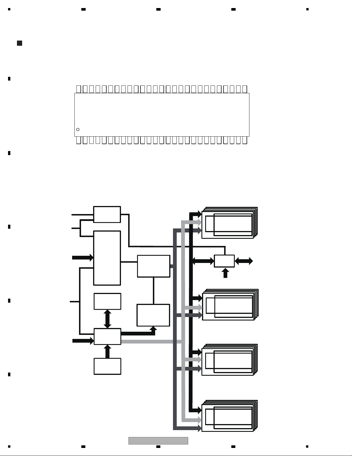
1. SERVICE PRECAUTIONS
1.1 NOTES ON SOLDERING
1.2 WHEN REPLACING MECHA ASSY
• For environmental protection, lead-free solder is used on the printed circuit boards mounted in this unit.
Be sure to use lead-free solder and a soldering iron that can meet specifications for use with lead-free solders for repairs
accompanied by reworking of soldering.
• Compared with conventional eutectic solders, lead-free solders have higher melting points, by approximately 40 ºC.
Therefore, for lead-free soldering, the tip temperature of a soldering iron must be set to around 373 ºC in general, although
the temperature depends on the heat capacity of the PC board on which reworking is required and the weight of the tip of
the soldering iron.
Do NOT use a soldering iron whose tip temperature cannot be controlled.
Compared with eutectic solders, lead-free solders have higher bond strengths but slower wetting times and higher melting
temperatures (hard to melt/easy to harden).
The following lead-free solders are available as service parts:
• Parts numbers of lead-free solder:
GYP1006 1.0 in dia.
GYP1007 0.6 in dia.
GYP1008 0.3 in dia.
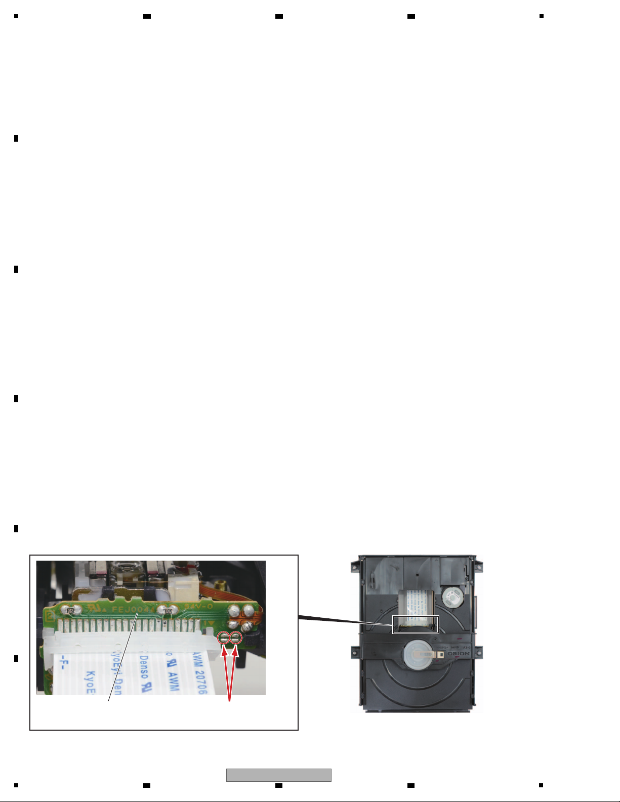
Fig. 1
Pickup PCB
Soldering short land
Short circuit using a soldering iron.
[ Removing the MECHA Assy ]
Before removing Pickup PCB and MAIN PCB Assy flexible cable, short circuit the two positions shown in Fig. 1 using
a soldering iron. If you remove the flexible cable with no soldering, the Laser may be damaged.
[ Installing the MECHA Assy ]
• Remove the soldering on the short circuit position after the connection of Pickup PCB and MAIN PCB Assy flexible cable.
Note:
• Use the Lead Free solder.
• Manual soldering conditions
Soldering temperature: 320 ± 20°C
Soldering time: Within 3 seconds
Soldering combination: Sn-3.0Ag-0.5Cu
• When Soldering/Removing of solder, use the draw in equipment over the Pickup Unit to prevent the Flux smoke from it.
5
PD-30-K
5
6 7 8
5
6 7 8
A
B
C
D
E
F
2. SPECIFICATIONS
General
System..............................................Super Audio CD player
Power requirements.......... AC 220 V to 230 V , 50 Hz/60 Hz
Power consumption
PD-30 ........................................................................37 W
PD-10 ........................................................................20 W
Power consumption (standby) .................................... 0.5 W
Weight
PD-30 ...................................................................... 5.4 kg
PD-10 ...................................................................... 5.1 kg
Dimensions.......... 435 mm (W) x 128 mm (H) x 329 mm (D)
Operating temperature ................................+5 °C to +35 °C
Operating humidity ............................................ 5 % to 85 %
(no condensation)
Audio output (1 stereo pair)
Output level.........................................During audio output
200 mVrms (1 kHz, –20 dB)
Number of channels ........................................................... 2
Jacks .............................................................................RCA
Digital audio characteristics
Frequency response
CD ..............................................................2 Hz to 20 kHz
SACD..........................................................2 Hz to 50 kHz
S/N ratio
CD .......................................................................... 117 dB
SACD......................................................................117 dB
Dynamic range
CD .......................................................................... 100 dB
SACD......................................................................108 dB
Total harmonic distortion:
CD ...................................................................... 0.0022 %
SACD..................................................................0.0020 %
Wow and flutter...................................Limit of measurement
(±0.001 % W. PEAK) or lower
Digital output
Optical digital output..........................Optical digital terminal
Coaxial digital output ....................................... RCA terminal
Note
• Specifications and the design are subject topossible
modifications without notice, due to improvements.
• Corporation and product names mentioned herein are
trademarks or registered trademarks of the respective
corporations.
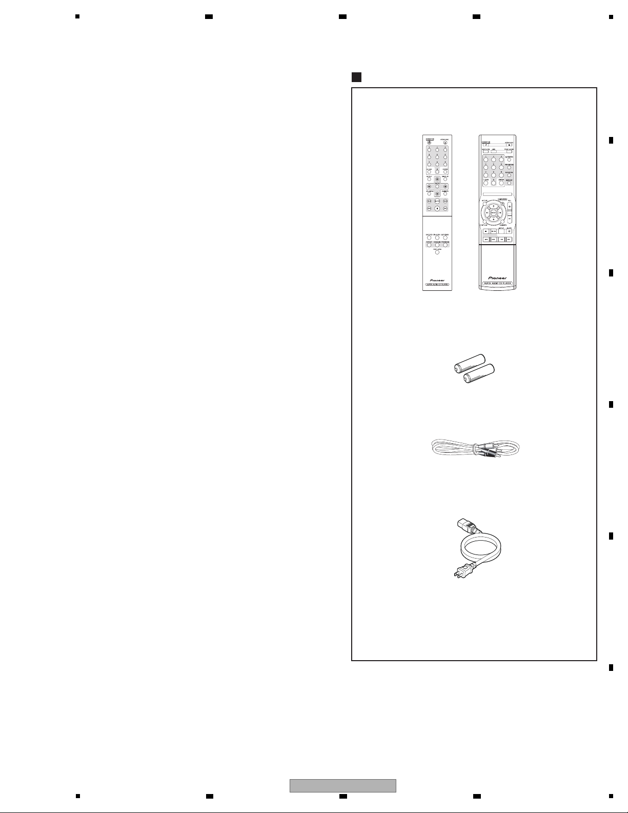
Remote control
(PD-30: 076D0UH011)
(PD-10: 076D0UI011)
PD-30 PD-10
AAA/IEC R03 dry cell batteries x2
RCA audio cable (red/white plugs)
(06EHBA2006)
Power cord
(PD-30: 120S154801)
(PD-10-K, PD-10-S: 120A158804)
(PD-10: ADG7097)
Warranty card
Operating Instructions
(PD-30, PD-10-K, PD-10-S: J1190171A)
(PD-10: J1180401A)
Accessories
6
PD-30-K
1
2 3 4
A
B
C
D
E
F
1
2 3 4
3. BASIC ITEMS FOR SERVICE
3.1 CHECK POINTS AFTER SERVICING
3.2 JIGS LIST
No. Check pointsProcedure
2
Confirm whether the customer complain has been solved.
The customer complain must not be reappeared.
Audio and operations must be normal.
1
Check the firmware version in the test mode.
The firmware version must be the latest one.
If it is not the latest one, be sure to update it.
3
Check the CD playback.
(Track search)
Audio and operations (search etc.) must be normal.
4 Check the SACD playback.
(Track search)
Audio and operations (search etc.) must be normal.
5
Check
the playback of the music file of supporting file format
with the USB port of the front.
Audio and operations (search etc.) must be normal.
Items to be checked after servicing
To keep the product quality after servicing, confirm recommended check points shown below.
6
Check the appearance of the product. No scratches or dirt on its appearance after receiving it
for service.
Item to be checked regarding audio
Distortion
Noise
Volume too low
Volume too high
Volume fluctuating
Sound interrupted
See the table below for the items to be checked regarding audio.
Cleaning
Name Part No. Remarks
Cleaning paper GED-008
Cleaning liquied GEM1004 Refer to "7. DISASSEMBLY".
Position to be cleaned
Pickup lens
Before shipping out the product, be sure to clean the following positions by using the prescribed cleaning tools.
Jigs List
Jig Name Part No. Remarks
Service remote control unit
GGF1381 Test mode
7
PD-30-K
5
6 7 8
5
6 7 8
A
B
C
D
E
F
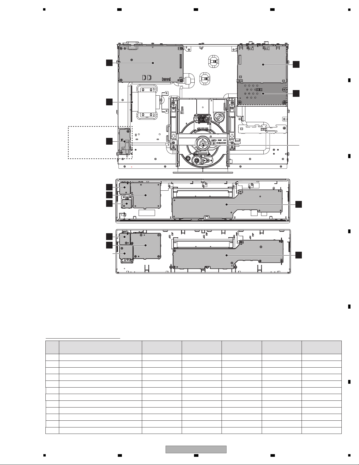
3.3 PCB LOCATIONS
LIST OF ASSEMBLIES
NOTES:
-
Parts marked by “NSP” are generally unavailable because they are not in our Master Spare Parts List.
-
The > mark found on some component parts indicates the importance of the safety factor of the part.
Therefore, when replacing, be sure to use parts of identical designation.
PD-30-K
/PWSYXZT8
Symbol and DescriptionMark
PD-30-S
/PWSYXZT8
PD-10-K
/PWSYXZT8
PD-10-S
/PWSYXZT8
PD-10
/FXZT
1..REMOCON PCB ASSY A11901ADA0 A11901ADA0 A11801ADA0 A11801ADA0 A11802ADA0
1..DISPLAY PCB ASSY A11901ADP0 A11901ADP0 A11801ADP0 A11801ADP0 A11802ADP0
1..LED PCB ASSY A11901ADT0 A11901ADT0 Not used Not used Not used
1..POWER 2 PCB ASSY A11901AFI0 A11901AFI0 A11801AFI0 A11801AFI0 A11802AFI0
1..MAIN PCB ASSY A11905AF40 A11901AF40 A11801AF40 A11801AF40 A11804AF40
1..AUDIO PCB ASSY A11905AF70 A11901AF70 A11801AF70 A11801AF70 A11802AF70
1..POWER PCB ASSY A11905A240 A11901A240 A11801A240 A11801A240 A11802A240
1..OPERATION PCB ASSY A11901A270 A11901A270 A11801A270 A11801A270 A11801A270
MECHA ASSY A11902A650 A11902A650 A11902A650 A11902A650 A11902A650
NSP 1..POWER SW PCB ASSY A11901A320 A11901A320 Not used Not used Not used
E
POWER PCB ASSY
F
POWER 2 PCB ASSY
H
POWER SW
PCB ASSY
D
REMOCON PCB ASSY
D
REMOCON PCB ASSY
OPERATION2 PCB ASSY
C
OPERATION PCB ASSY
C
OPERATION PCB ASSY
I
LED PCB ASSY
PD-30 only
for PD-30
for PD-10
B
AUDIO PCB ASSY
A
MAIN PCB ASSY
G
DISPLAY
PCB ASSY
G
DISPLAY
PCB ASSY
MECHA ASSY
8
PD-30-K
1
2 3 4
A
B
C
D
E
F
1
2 3 4
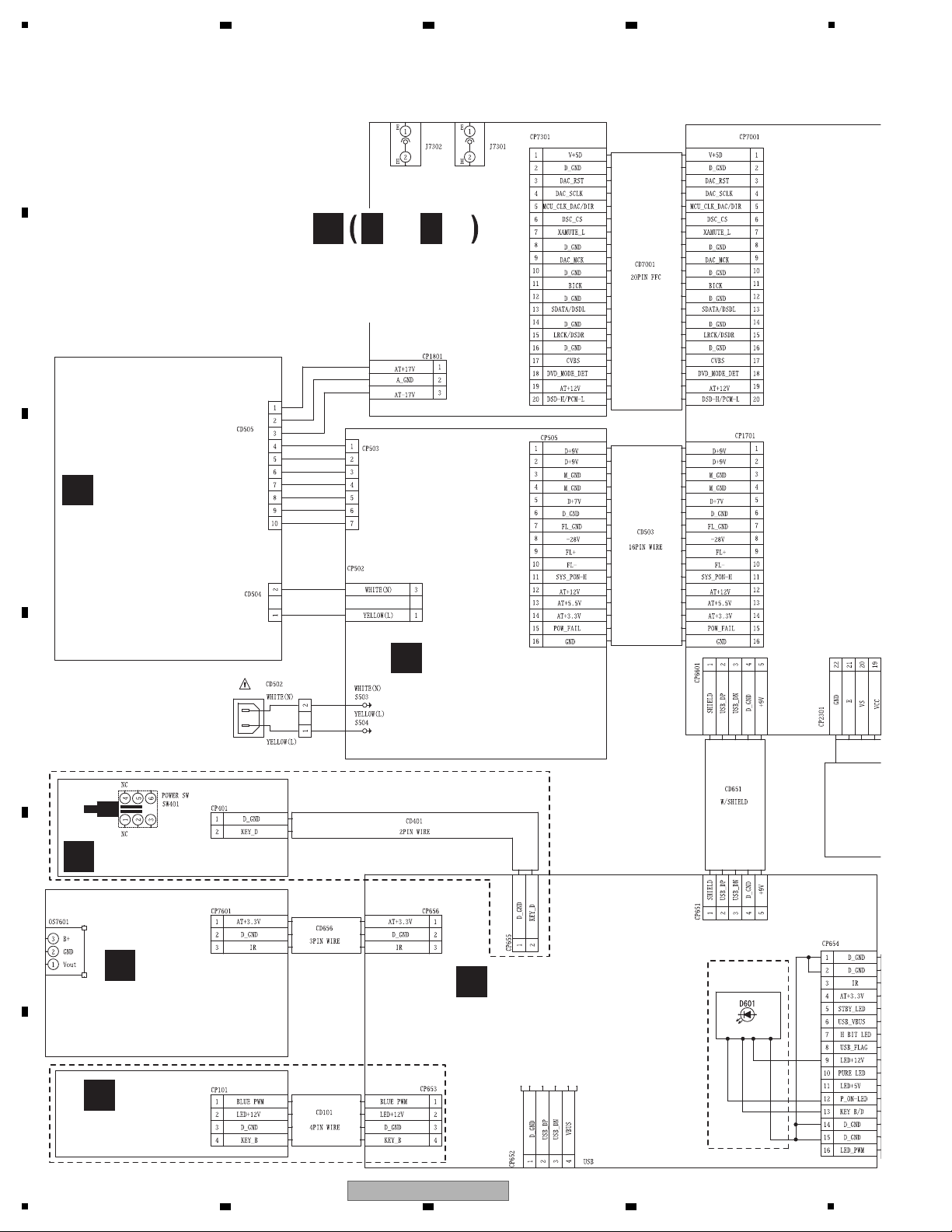
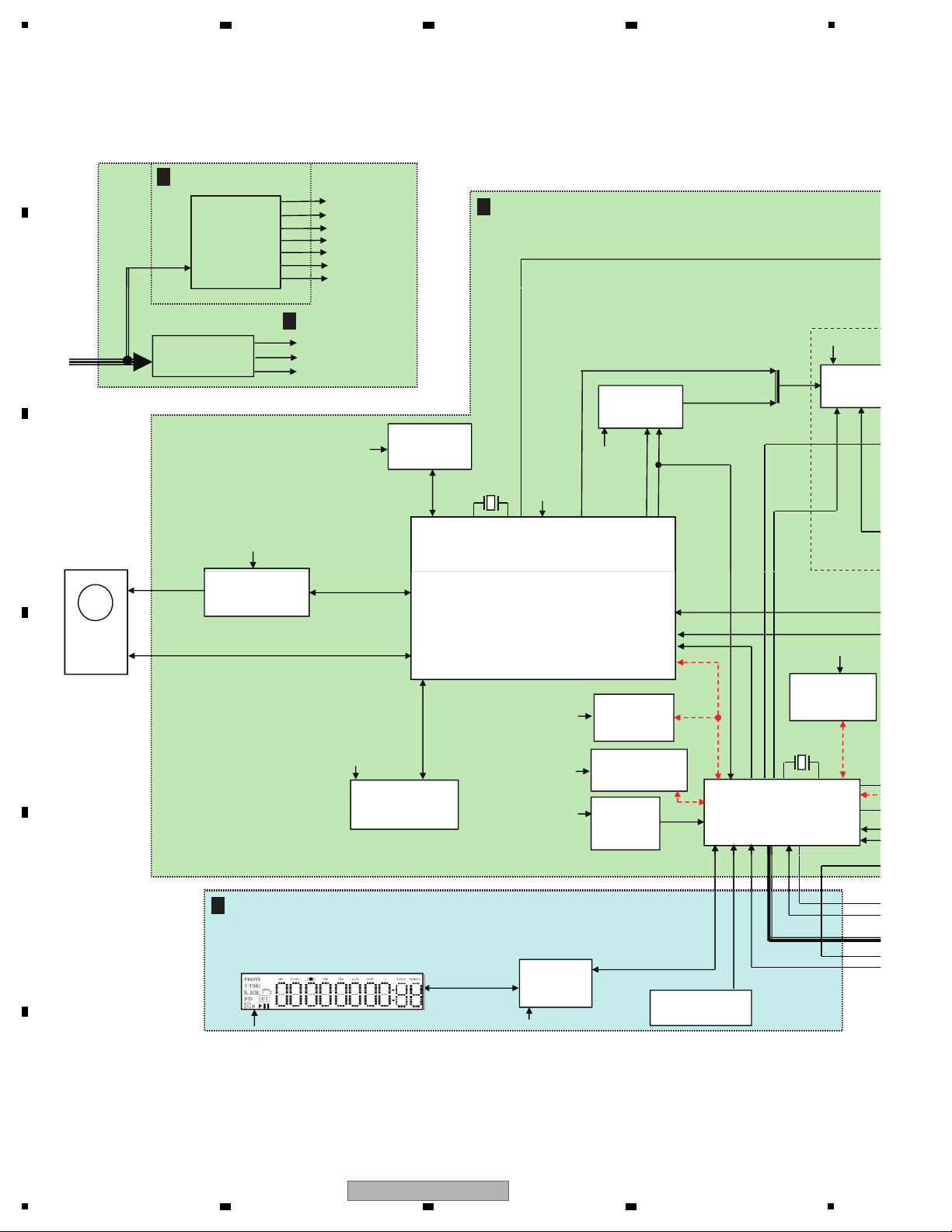
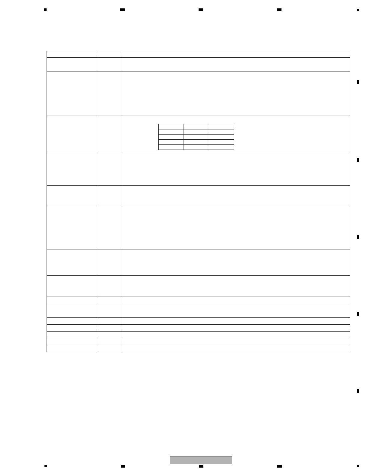
4. BLOCK DIAGRAM
4.1 OVERALL WIRING DIAGRAM
OPERATION PCB ASSY
(PD-30: A11901A270)
(PD-10: A11801A270)
C
POWER PCB ASSY
E
POWER 2 PCB ASSY
F
REMOCON PCB ASSY
D
POWER SW PCB ASSY
(A11901A320)
PD-30 ONLY
PD-30 ONLY
H
LED PCB ASSY
(A11901ADT0)
I
AUDIO PCB ASSY
(PD-30: A11905AF70)
(PD-10-K, PD-10-S: A11801AF70)
(PD-10: A11802AF70)
B
B
1/2,
B
2/2
(PD-30: A11901ADA0)
(PD-10-K, PD-10-S: A11801ADA0)
(PD-10: A11802ADA0)
(PD-30: A11905A240)
(PD-10-K, PD-10-S: A11801A240)
(PD-10: A11802A240)
(PD-30: A11901AFI0)
(PD-10-K, PD-10-S: A11801AFI0)
(PD-10: A11802AFI0)
OPERATION2
PCB ASSY
PD-10 ONLY
9
PD-30-K
5
6 7 8
5
6 7 8
A
B
C
D
E
F
MAIN PCB ASSY
(PD-30: A11905AF40)
(PD-10-K, PD-10-S: A11801AF40)
(PD-10: A11804AF40)
A
DISPLAY PCB ASSY
(PD-30: A11901ADP0)
(PD-10-K, PD-10-S: A11801ADP0)
(PD-10: A11802ADP0)
MECHA ASSY
(A11902A650)
G
A
1/8-
A
8/8
-
When ordering service parts, be sure to refer to "EXPLODED VIEWS and PARTS LIST" or "PCB PARTS LIST".
-
The > mark found on some component parts indicates the impor tance of the safety factor of the part.
Therefore, when replacing, be sure to use parts of identical designation.
10
PD-30-K
1
2 3 4
A
B
C
D
E
F
1
2 3 4
4.2 OVERALL BLOCK DIAGRAM
EI TRANS
T502
+17V
M+7V
-28V
-17V
FLDC+
FLDC-
+9V
M+6V
64Mbit SDRAM
IC4002
EM638165TS-6G
27MHz
X4001
TRCLOSE/TROPEN
DMSO/FOSO/STBY
MA0 - MA11
DQ0 - DQ15
S
IC
TC74V
AC 100V/110V
or
AC 220V - 240V
Switching TRANS
T501
AT+3.3V
SW IC
IC7001
TC7SB3157CF
DSD-H
/PCM-L
ALRCK
DSD-R
MPEG_MCK
ABCK
DATA0/DSD-L
SW1
ALRCK/DSD-R
+3.3V
+3.3V
+1.8V
AT+5V
AT+12V
+3.3V
+3.3V
LOADING
SPINDLE
FOCUS
TRACKING
I2C BUS
CD u-com
IC4001
MT1389JE/S-L
16Mbit FLASH IC
IC4003
EN29LV160BB-70TIP
(DM-5)
IC2301
MOTOR DRIVER
SA5888TR
DMSO/FOSO/STBY
TRSO/FMSO/TRPWM
RF, LD_DVD,
4K EEPROM
IC4004
FT24C04A-
RESET IC
IC3002
R3112N291A
RESET
A0 - A20
SUB MICON
IC3001
M3030SFEPGP
(ROM: 192K, RAM12K)
I2C BUS
89S_RESET
16MHz
X3002
IR
Apple IC
IC3004
341S2162-TBB
I2C BUS
2K EEPROM
IC3003
FT24C02A-USG
+3.3V
+3.3V
+3.3V
TRACKING
SLED
AT+3.3V
AT+3.3
Ef=4V, eb=ec=-28V
V+3D, -28V
P1 - P16
GR1 - GR11
VFD DRIVER
IC6001
SC16315
FP_DI/FP_DO
FP_SCK/STB
SW
SW6001 - SW6006
VFD V6001
11-BT-226GNK
KEY_A/C
KEY_D
F POWER 2 PCB ASSY
MECHA ASSY
E POWER PCB ASSY
A MAIN PCB ASSY
G DISPLAY PCB ASSY
PD-30 ONLY
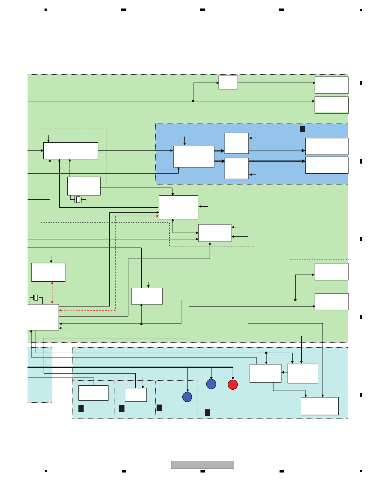
11
PD-30-K
5
6 7 8
5
6 7 8
A
B
C
D
E
F
ASPDIF
BUFFER
COAXTIAL OUT
J7001
RCA-125-01
OPTICAL OUT
OS7001
216kHz/32bit DAC
IC7301
AK4480
SW IC
IC7002
TC74VHC157FT
iPod CTL
IC6601
BU94604BKV
IPOD_SDATA
IPOD_BCK
IPOD_LRCK
16.934MHz
X6601
OPAMP
IC7303
NJM5532M
OPAMP
IC7302
NJM5532M
SW1
BUFF
IC6603
TC7WU04FU
+3.3V
+3.3V
IPOD_MCK
IPOD_MCK
OPT-103B-01
AUDIO JACK (L CH)
J7302
RCA-125F-WH
AUDIO JACK (R CH)
J7301
RCA-125F-RD
±15V
±15V
+5V
DAC_MCK
BICK
SDATA/DSDL
LRCK/DSDR
DAC_RST
MCU_CLK_DAC/DIR
MCU_DO_DAC/DIR
MCU_CS_DAC
+3.3V
+3.3V
I2C BUS
16MHz
X3002
IR
AND GATE
IC3005
TC7SH08FU
USB SW
IC6602
TC7USB221FT
MPEG_DP/DN
USB_DP/DN
SR IN
I2C BUS
2K EEPROM
IC3003
FT24C02A-USG
+9V
IPOD_CTL_RESET
AT+3.3V
SR IN
J7003
PJ-308-01-BK
SR OUT
J7002
PJ-308-01-BK
USB_EN
USB_SW
IPOD_DP/DN
AT+3.3V
FLAG
EN
IR
OS7601
USB
CONNECTOR
CP652
High Side SW
IC654
TPS2557DRB
3A DC/DC(5V)
IC651
RT8293AHZS
VBUS 5V
PURE
AUDIO
STANDBY
POWER
ON
POWER SW
SW401
IR IN
AT+3.3V
B AUDIO PCB ASSY
C OPERATION PCB ASSY
D REMOCON
PCB ASSY
H POWER SW
PCB ASSY
I LED PCB ASSY
PD-30 ONLY PD-30 ONLY
PD-30 ONLY
PD-30 ONLY
PD-30 ONLY
12
PD-30-K
1
2 3 4
A
B
C
D
E
F
1
2 3 4
4.3 POWER BLOCK DIAGRAM
W/HEATSINK
+5V REG
SYS_PON-H
SYS_PON-H
6V DC-D
D+7V
IC1709
IC1701 PDIC
RT8292BHGSP KIA278R05PI
LD
COAXTIAL DRV
Q7002
3.3V REG
V+3
V+5S
V+5D
IC1702
MPEG IC4001
RP131H331D-T1-F
MT1389EE/S-L
1.8V REG
V+1R8
3.3V REG
IC1708
IC1703
RP131H331D-T1-F
RP131H181D-T1-F
EEPROM(MPEG) IC4004
FT24C04A-USG-T
64Mbit SD-RAM IC4002
EM638165TS-6G(70NM)
16Mbit FLASH IC4003
EN29LV160BB-70TIP
D6V
6V DC-DC
MOTOR DRIVER IC2301
D+9V
IC1710 SA5888TR
RT8292BHGSP
OPTICAL OS7001
OPT-103B-01
AND GATE IC3005
TC7SH08FU
AUTHE
NTIC
ATION IC
IC3004 341S2164-TBB
IPOD DECODE
IC6601 BU94694KV
USB SW
IC6602 TC7USB221FT
IPOD/CD SW
IC7002 TC74VHC157FT
DSD/PCM SW
IC7001 TC7SB3157CFU
5V DC-DC
High Side SW
USB
IC1704
IC654
CP652
RT8293AHZSP TPS2557DRB
C-001-1-4K22400
FIP DRIVER
-28V
REG
REG
Q1701
Q1708
FL-DC+ FIP
FL-DC-
W/HEATSINK
USB_VBUS
AC+17V
5V Reg
V+5A
Audio DAC IC7301
IC1801
AK4480
NJM78M05FA
+15V Reg V+15A
Audio
IC1802 IC7302/IC7303
NJM78M15FA
NJM5532M
AC-17V
-15V Reg
V-15A
IC1803
NJM7
9M15FA
AT+3 .3V SUB MICON IC3001
M3030SFEPGP
EEPROM(MICON) IC3003
FT24C02A-USG-T
AT+5 .5V LED (BLUE/RED)
D101/D656/D659
AT+1 2V
E
POWER
PCB ASSY
MECHA ASSY
B
AUDIO PCB ASSY
C
OPERATION PCB ASSY
13
PD-30-K
5
6 7 8
5
6 7 8
A
B
C
D
E
F
5. DIAGNOSIS
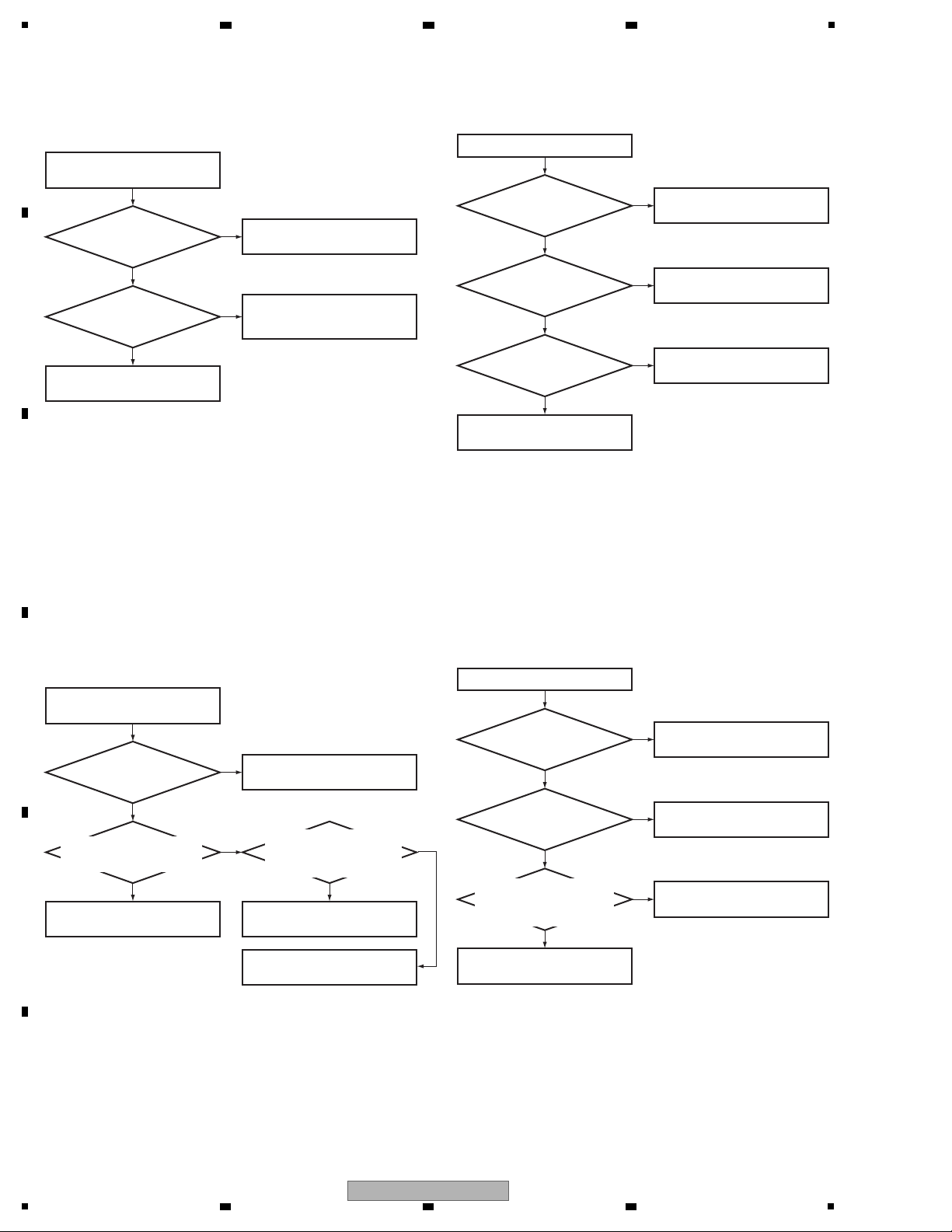
5.1 TROUBLESHOOTING
Power does not turn on
Ye s
Power does not turn on
Is the voltage of CP1701
pin 14 about 3.3 V?
Is the voltage of IC3001
pin 18 about 3.3 V?
No
Check the T501 (POWER PCB)
and around circuits.
No
Check the Q1707 and Q1709.
Ye s
Is the voltage of CP1701
pin 11 about 3.3 V?
No
Check the IC3001 and arround
circuits.
Ye s
Is the voltage of Q502
collector 0 V?
Ye s
No
Check the Q502.
Replace the POWER PCB Assy.
Display is not displayed
Ye s
Display is not displayed
Are the voltages of IC6001
pin 13, 43 about 3.3 V?
Is the voltage of IC6001
pin 30 about -28 V?
No
Check the V+3 line of
regulator block.
No
Check the Q1703, Q1701 and
arround circuits.
Ye s
Are the voltages of V6001
pin 1, 2 about -23 V?
Are the voltages of V6001
pin 34, 35 about -19 V?
No
Check the FL_DC+/FL_DC- line of
regulator2 block
arround circuits.
Ye s
Replace the V6001 or IC6001.
Tray does not open / close
Ye s
Tray does not open/close
Are the voltages of IC2301
pin 8, 19 DC 6 V?
Are MECHA Assy and CP2302
connected?
No
Check the D6V line of
regulator block.
No
Check connection of MECHA Assy
and CP2302.
Ye s
Is the voltage of CP1701
pin 11 about 3.3 V?
No
Check the IC3001 and arround
circuits.
Ye s
Replace the MECHA Assy.
DIGITAL OUT is not output by DIGITAL OUT
(COAXIAL) at the CD playback
Ye s
DIGITAL OUT is not output by
DIGITAL OUT (COAXIAL)
at the CD playback
Is waveform of J7001 pin 2
0.5 Vp-p?
Is waveform of IC4001
pin 215 0.5 Vp-p?
No
Check connection of audio cable.
No
Check the Q7002 and arround
circuits.
Ye s
Replace the IC4001.
14
PD-30-K
1
2 3 4
A
B
C
D
E
F
1
2 3 4
DIGITAL OUT is not output by DIGITAL OUT
(OPTICAL)
Ye s
DIGITAL OUT is not output by
DIGITAL OUT (OPTICAL)
Is the voltage of OS7001
pin 2 about 3.3 V?
Is waveform of OS7001
pin 1 3.3 V?
No
Check the V+3 of regulator
block J.
No
See "DIGITAL OUT is not output
by DIGITAL OUT (COAXIAL) at
the CD playback".
Ye s
Replace the OS7001.
Ye s
Replace the IC4001.
USB does not playbak
Ye s
Is the voltage of CP652
pin 1 about DC 5 V?
OPERATION and MAIN
PCB Assy connected?
No
Check the IC654 pin 2 to 4 and
around circuits.
Are the voltages of IC6602
pins 1, 7 about 3.3 V?
No
Check the Q6602, Q6603, IC3001
and around circuits.
Check connection.
No
Ye s
Sound (ANALOG OUT) is not output by Analog out
terminals at playback
Ye s
Sound (ANALOG OUT) is not output
by Analog out terminals at playback
Is the signal output by
IC7302/IC7303 pin 1?
Are the waveforms of
IC7301 pins 10, 11, 20, 21
output?
Is the voltage of IC7302
pin 8 about 15 V?
Is the voltage of IC703/IC7302
pin 4 about -15 V?
No
Check the Q7308/Q7312/Q7304
/Q7311 and around circuits.
No
Check the V;15A, V-15A lines of
AUDIO POWER.
No
Ye s
Check the IC7301 and around
circuits.
Ye s
Check the IC7301/IC7303 and
around circuits.
USB does not playbak
Ye s
Check the IC6601 and
around circuits.
iPod does not playbak (PD-30 only)
Ye s
Is the voltage of CP652
pin 1 about DC 5 V?
OPERATION and MAIN
PCB Assy connected?
No
Check the IC654 pin 2 to 4 and
around circuits.
Is the voltage of IC6602 pin 1
about 3.3 V?
Is the voltage of IC6602 pin 7
about 0 V?
No
Check the voltages of Q6602,
Q6603, IC3001.
Check connection.
No
Ye s
iPod does not playbak
15
PD-30-K
5
6 7 8
5
6 7 8
A
B
C
D
E
F
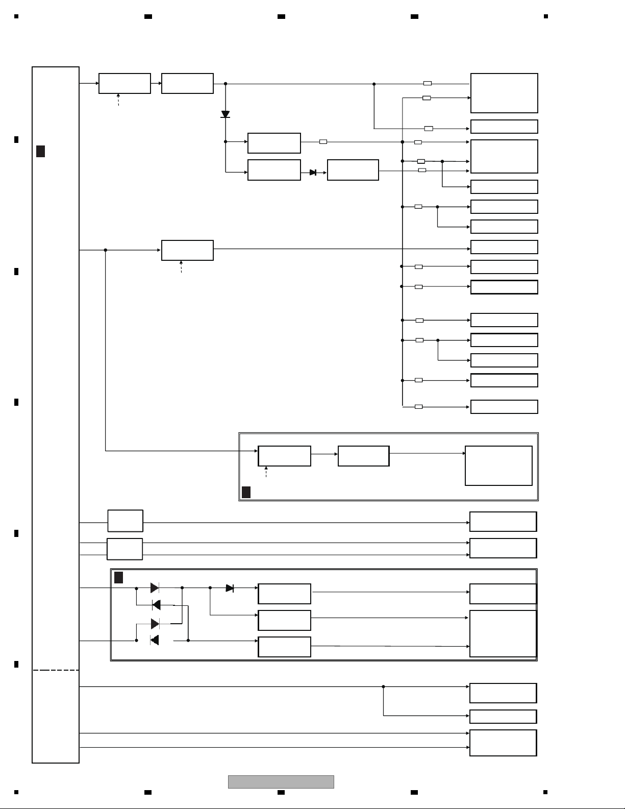
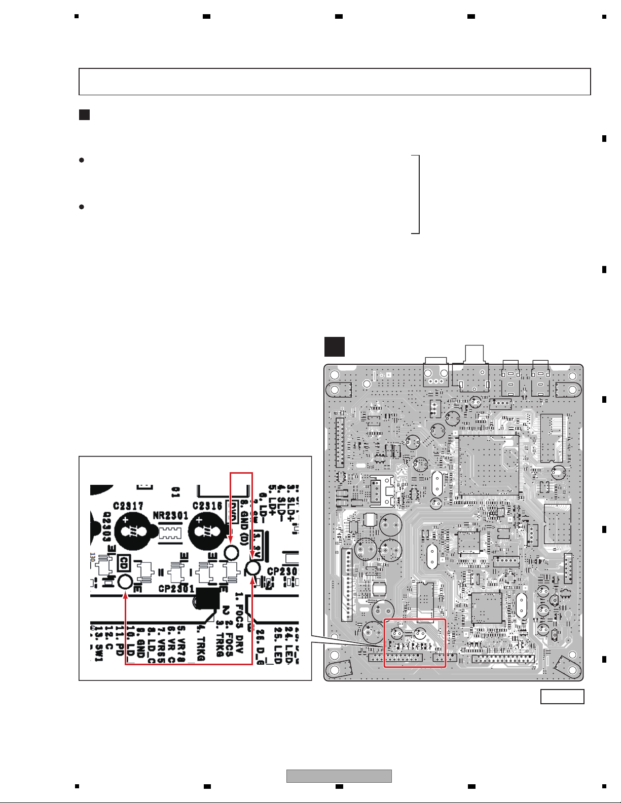
5.2
METHOD FOR DIAGNOSING DEGRADATION OF THE LDS ON THE PICKUP ASSY
117
33
49
1
51
76
26
11
16
16
129
193
1
65
R3030
SH1701
R3031
SH1702
R3032
R3033
SH1703
R3034
SH1704
R3035
R3036
R3037
R3038
C4001
R3039
C4002
W807
C4003
C4004
C4005
Q4001
C4006
Q4002
C4007
Q4003
C4008
R3040
C4009
R3041
Q1701
C1706
R3042
C1707
R3043
Q1703
C1708
R3044
W810
W811
C1709
R3045
Q1705
R3046
Q1706
Q1707
R3047
W813
W814
R3048
Q1708
Q1709
C4011
R3049
W815
C4012
C4014
C1711
C4015
C1712
C4016
C1713
C4017
C4018
C1714
R3050
C4019
R3051
R3052
R3053
R3054
W820
W821
R3055
R3056
R3057
C4020
R3058
C4021
C4022
W827
C4024
W829
C4026
C4027
R4001
C4029
R3061
B2301
R4002
R3062
R4003
R3063
R4004
R3064
R4005
NR2301
D1705
R4006
R1702
R4007
R3067
R1703
R4008
C4030
R3068
D1708
W834
R4009
C4031
R3069
IC400 2
IC400 3
IC400 4
C4034
W838
IC170 1
HS1701
C4035
C4036
IC170 2
IC170 3
C4037
R4010
C4038
D1710
C4039
R4011
D1711
R4012
D1712D1713
R3073
C1737
R4013
IC170 8
D1714
R4014
R3074
C1738
CP4001
IC170 9
R3075
D1715
R4016
CP4002
R3076
R3077
R4017
R3078
C4040
R4018
R1714
R4019
C4041
CP1701
C4043
R1717
C4044
IC171 0
IC171 1
C4045
C4046
C4047
R4021
C4049
R4022
R4023
R4024
W850
R1720
R4025
C1749
R4026
C2302
W852
C2303
C4050
C2305C2306
R1726
Q2303
R1727
C4054
Q2304
R1728
C4055
Q2305
R1729
C4056
Q2308
C4058
R4030
Q2309
C4059
R4032
R4033
C1757
R4034
W860
R1730
R4035
C2311
R1731
R4036
C2312
R1732
R4037
R1733
C2313
W863
Q2310
C4060
R4038
C2314
Q2311
C2315
C4053_1
C4062
C2316C2317
W867
R1738
C1760
W868
C2319
C1761
W869
C4066
C1762
R4040
C1764
C4068
R4041
C4069
R4042
R4043
R4044
C1768
R4045
W871
R4046
C2322
W872
R4047
C2323
W873
R4048
C2324
W874
C2325
C4073
C4074
C4075
R2301
R1749
C4076
R2302
C4077
C1773
R4050
C4078
C4079
C1775
C4057_1
C1776
R2306
R2307
R2308
R1751
C1779
IC230 1
R1752
W882
C4080
R1754
R4058
W884
C4083
W887
C4084
W888
C4085
R1759
W889
C4086
R2312
C1782
C4087
C1783
R2313
R4060
C4088
R2314
R4061
C1785
R2315
CP2301
R2316
CP2302
C1786
R2317
C1787
R2318
C1788
W890
W891
R2319
R1761
C1789
C4090
R1765
C4091
W895
C4093
W898
C4094
R2320
W899
C1793
C1794
R1770
R1771
R1772
X3002
R1779
C4061_1
B6601
B6602
B6603
C4067_1
C6601
C6603
C6604
C6605
Q6602
C6606
C6608
C6609
C6612
C6614
B7001
B7002
W903
W904
B7004
W905
X4001
B7005
B7006
W906
W908
W909
C6624
W911
W912
W914
IC660 1
IC660 2
IC660 3
C6635
C6637
R6610
R6612
R6613
C7001
CP6601
C7002
C6640
C7004
Q7001
R6619
C7005
C7006
Q7002
C7008
C7009
R6620
R6621
R6622
R6623
R6624
C7010
C7011
R6625
C7012
R6626
C7013
C7014
R6628
C4136
C4137
C4139
R6630
R6632
R6633
C4140
C4141
R6635
R6636R6637
C7024
R6638
C4144
R6639
D7001
C4145
C4146
D7002
D7003
R7001
L1701
C2304_1
R7002
L1702
R7003
R7004
R7005
R6641
R7006
R6642
R7007
R6643
R6644
R7008
R6645
IC700 1
R7009
IC700 2
R6647
R6648
C4155
R6649
C4157
R7010
R7011
R7012
R7013
R7014
R7015
CP7001
R7016
R7017
R7018
R6656
R6657
R7020
C4168
R7025
R7026
R7027
R7028
OS7001
B3009
C3002
Q3001
C3005C3006
C3007
C3009
C3012
C3014
C3015
C3016
C3024
D3001
C3026
R3001
R3003
R3004
D3008
D3009
C3030
IC300 1
R3009
IC300 2
C3033
IC300 3
D3010
IC300 4
IC300 5
C3036
C3037
R3012
R3013
R3014
R3015
CP3001
R3016
CP3002
CP3003
R3017
R3018
R3019
NR4002
B1702
B1703
B4008
NR4004
B1704
C3044
B4009
C3046
B1706
C3047
C3048
R3020
R3022
B4010
B4012
R3026
R3027
R3028
C3050
R3029
X6601
J7002 J7003
J7001
IC400 1
A
MAIN PCB ASSY
SIDE A
Case when this diagnosis is required:
When playback of any disc, including a test disc (DVD: GGV1025 (NTSC) / GGV1101 (PAL), CD: STD-905), cannot be performed
In the case mentioned above, degradation of the laser diodes (LDs) mounted on the PICKUP Assy is suspected.
Measure the voltage between the two ends of one of the resistors mentioned below.
Measure the voltage between DVD TP and 3.3V TP on the MAIN PCB Assy.
If the voltage is 0.17 V or higher, the 650-nm LD is degraded.
If the measurements show degradation
of an LD, replace the MECHA Assy.
CD
DVD
How to diagnose
No playback of a DVD:
Measure the voltage between CD TP and 3.3V TP on the MAIN PCB Assy.
If the voltage is 0.20 V or higher, the 780-nm LD is degraded.
No playback of a CD:
16
PD-30-K
1
2 3 4
A
B
C
D
E
F
1
2 3 4
5.3 IC INFORMATION
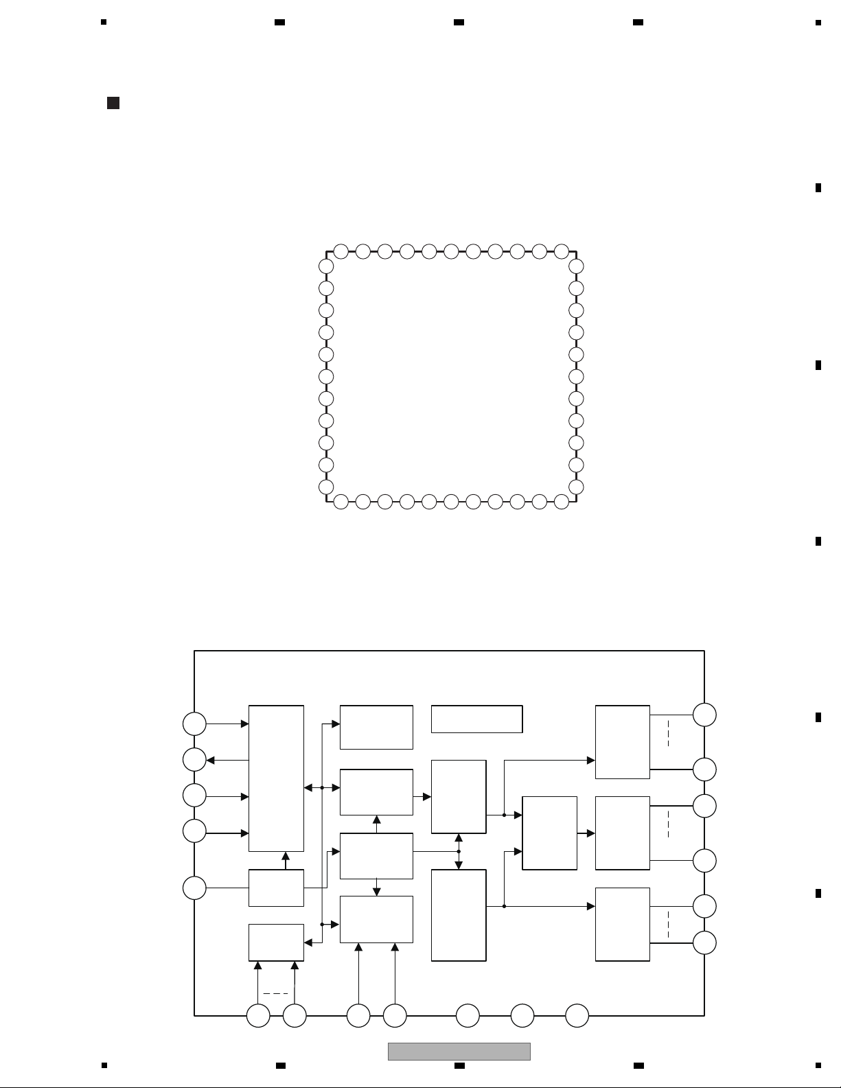
Energy Effi cient, Offl ine Switcher with Enhanced Flexibility and Extended Power Range
• Block Diagram
• Pin Arrangement
CLOCK
OSCILLATOR
5.85 V
4.9 V
SOURCE
(S)
S
R
Q
DC
MAX
BYPASS/
MULTI-FUNCTION
(BP/M)
+
-
V
I
LIMIT
FAULT
PRESENT
CURRENT LIMIT
COMPARATOR
ENABLE
LEADING
EDGE
BLANKING
THERMAL
SHUTDOWN
+
-
DRAIN
(D)
REGULATOR
5.85 V
BYPASS PIN
UNDER-VOLTAGE
1.0 V + V
T
ENABLE
(EN)
Q
115 A
RESET
AUTO-
RESTART
COUNTER
JITTER
BYPASS
CAPACITOR
SELECT AND
CURRENT
LIMIT STATE
MACHINE
OVP
LATCH
1.0 V
D
S
BP/M
S
S
EN
8
5
7
1
4
2
S
6
ILDF0176P0 (TNY176PN)(POWER PCB ASSY: IC501)
17
PD-30-K
5
6 7 8
5
6 7 8
A
B
C
D
E
F
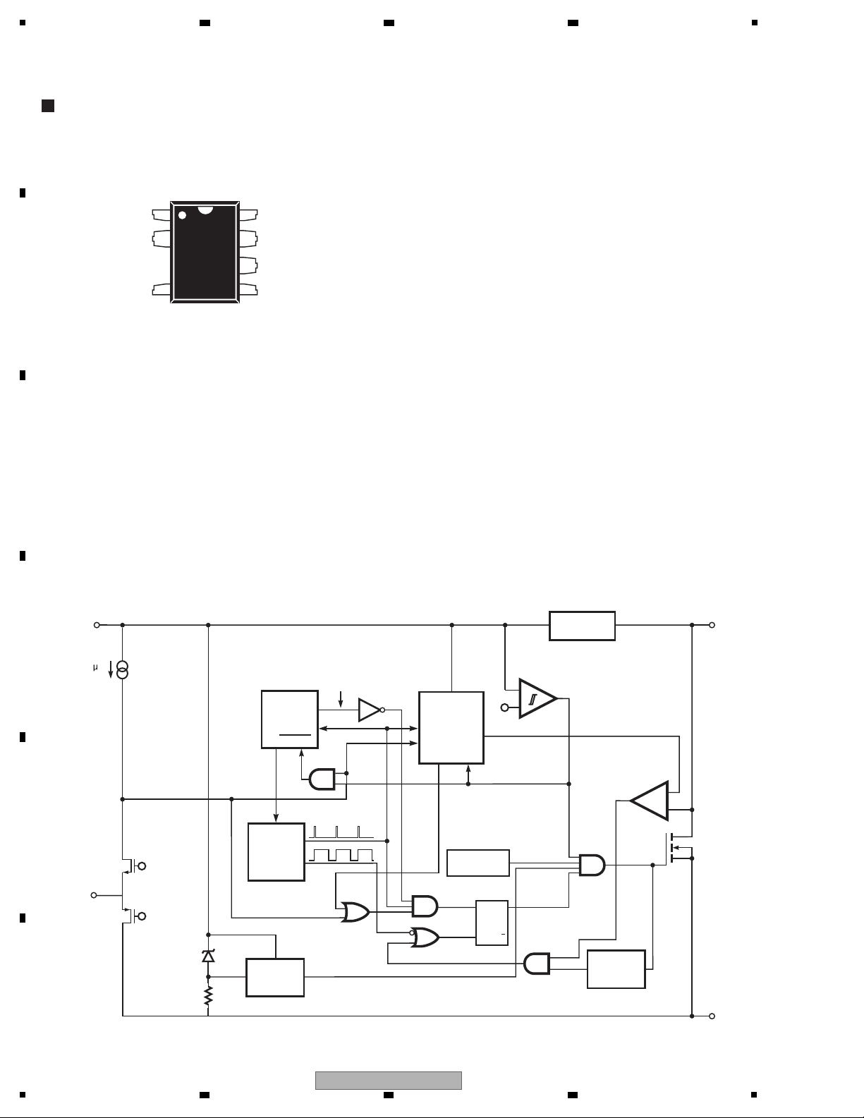
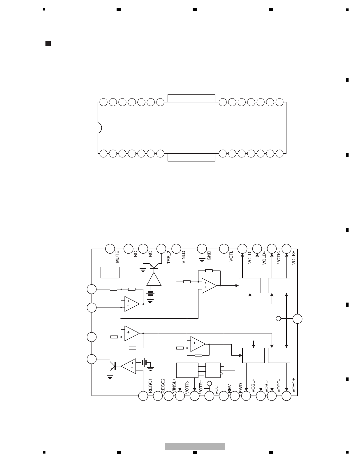
5CH MOTOR DRIVER IC
• Block Diagram
• Pin Arrangement
1 2 3 4 5 6 7 8
16 15
14131211109
28 27 26 25 24 23 171819202122
SA5888
VINFC
TRB_1
REGO2
V
IN
SL
+
REGO1
FWD
REV
V
CC
VOTR-
VOTR+
VOSL+
VOFC-
VOSL-
VOFC+
MUTE
TRB_2
V
IN
TK
NC
V
IN
LD
GND
VCTL
NC
PVCC
VOLD-
VOTK-
VOLD+
VOTK+
BIAS
1
28
VINFC
2
5
Mute
26
27
3
+-
2520
4 9 10
Tray
Driver
Pre-
DRV
8 7 6 11 12
Sled
driver(4x)
23 2122 18 17
Spindle
Driver(4x)
16 15
Actuator
Driver(6x)
Actuator
Driver(6x)
13 14
TRB_1
VCC
VCC
PVCC
24
10K
25K
25K10K
VINTK
BIAS
10K
15K
25K
10K
19
PVCC
I1UFV5888S (SA5888TR)(MAIN PCB ASSY: IC2301)
18
PD-30-K
1
2 3 4
A
B
C
D
E
F
1
2 3 4
• Pin Function
Pin No. Pin Name Description
1 VINFC Focus driver input
2 TRB_1 Connect to external transistor base
3 REGO2 Regulator voltage output, connect to external transistor collector
4 VINSL+ Sled driver input
5 REGO1 Regulator voltage output, connect to external transistor collector
6FWD Tray driver forward input
7REV Tray driver reverse input
8VCC VCC
9 VOTR- Tray driver output(-)
10 VOTR+ Tray driver output(+)
11 VOSL+ Sled driver output (+)
12 VOSL- Sled driver output (-)
13 VOFC- Focus driver output (-)
14 VOFC+ Focus driver output (+)
15 VOTK+ Tracking driver output (+)
16 VOTK- Tracking driver output (-)
17 VOLD+ Spindle driver output (+)
18VOLD- Spindle driver output (-)
19 PVCC Vcc for power block of spindle, tracking and focus
20 NC No connection
21 VCTL Speed control input of tray driver
22 GNDGround
23 VINLD Spindle driver input
24 NC No connection
25 TRB_2 Connect to external transistor base
26 VINTK Tracking driver input
27 BIAS Bias input
28 MUTE Mute control
Notes: The indicated polarities for the output pins are means polarity to inputs.
Always ensure that V
CC PVCC
19
PD-30-K
5
6 7 8
5
6 7 8
A
B
C
D
E
F
MEMORY DATA 192K/12K SINGLE CHIP MICON
• Block Diagram
• Pin Arrangement
Port P0
Additional function
Timer (16 bits)
Output (Timer A) 3 line
Input (Timer B) 3line
Watch dog timer
(15 bits)
A/D converter
(10 bits x 18 channel)
M16C/60 series CPU core
Memory
System clock genarate
XIN-XOUT
XCIN-XCOUT
UART or Clock sync
serial I/O
(3 channel)
CRC operation circuit (CCITT system)
(generation many clauses expression:
X
16
+ X
12
+ X
5
+ 1
DMAC
(2 channel)
8
Port P1
8
Port P2
8
Port P3
8
Port P4
8
Port P5
8
Port P6
8
Port P7
8
Por t P 8
8
Por t P 8_5
8
Port P9
8
Port P10
8
R0H R0L
R1H
R2
R3
A0
SB
INTB
PC
USP
ISP
FLG
ROM
RAM
multiplier
A1
FB
R1L
(M3030SFEPGP)(MAIN PCB ASSY: IC3001)
20
PD-30-K
1
2 3 4
A
B
C
D
E
F
1
2 3 4
• Pin Function
Category Pin Name I/O Function
Power supply
input
VCC1, VCC2,
VSS
I/O Input 2.7 V - 5.5 V into VCC1, VCC2. The input condition is VCC1 = VCC2.
Input 0 V into VSS.
Analog power supply
input
AVCC, AVSS I Power supply input of the A/D converter.
Connect AVCC to VCC1. Connect AVSS to VSS.
I
2
C mode SDA0 - SDA2 I/O Serial data input and output. (but the output of SDA2 is N channel open drain.)
SCL0 - SCL2 I/O Transfer clock input and output. (but the output of SCL2 is N channel open drain.)
Serial interface
CTS0 - CTS2
I Transmission system order input.
RTS0 - RTS2
O Reception system order output.
CLK0 - CLK2 I/O Transfer clock input and output.
RXD0 - RXD2 I Serial data input.
TXD0 - TXD2 O Serial data output. (but the output of TXD2 is N channel open drain.)
CLKS1 O Output of the transfer clock plural terminal output function.
Timer B TB0IN - TB2IN I Timer B0 - B2 input.
Timer A TA0OUT - TA2OUT I/O
Input and output of timer A0 - A2. (but the output of TA0OUT is N channel open drain.)
TA0IN - TA2IN I Timer A0 - A2 input.
Key input interrupt input
KI0 - KI3
I Input of the key input interrupt.
NMI interrupt input NMI
I
Input of the NMI interrupt.
INT interrupt input INT0 - INT4
I
Input of the INT interrupt.
Clock output CLKOUT O Output the clock of the period same as fc, f8 or f32.
Main clock input XIN I
Main clock output XOUT O
Input and output terminals of the main clock oscillation circuit. Connect a ceramic
resonator or a crystal oscillation child between XIN and XOUT. When you input a
clock formed outside, input a clock from XIN, and perform XOUT for open.
Sub clock input XCIN I
Sub clock output XCOUT O
Input and output terminals of the subclock oscillation circuit. Connect a crystal
oscillation child between XCIN and XCOUT. When you input a clock formed outside,
input a clock from XCIN, and perform XCOUT for open.
ALE O Signals for a latch to do an address.
HOLD
I
The microcomputer becomes the hold state the input of this terminal during a period of "L".
WRL/WR,
WRH/BHE,
RD
O
Output WRL, WRH (WR, BHE), RD signals. Be changed WRL, WRH or BHE, WR by
a program.
· at WRL, WRH, RD selected
In case of external data bus is 16 bits, WRL signal is "L", writes it in the even
number address, and WRH signal is "L", writes it in the odd number address.
· at WR, BHE, RD selected
WR signal is "L", writes. RD signal is "L", read. BHE signal is "L", accesses it by
an odd number house number.
Use this mode at the external data bus is 8 bits.
CS0 - CS3
O Chip select signals. Use it for designation of the access space.
A0 - A19 O Output address A0 - A19.
Bus control pin D0 - D7 I/O When accessed the area selecting a separate bus, input and output data (D0 - D7).
D8 - D15 I/O When an external data bus accessed it in an area selecting a separate bus at 16 bits,
input and output data (D8 - D15).
External data bus
switch input
BYTE I Be terminals to switch an external data bus. In the case of "L" this terminal becomes
16 bits, in the case of "H" this terminal becomes 8 bits.
Fix it to either. Be connected to VSS with the single chip mode.
CNVSS CNVSS 0 Be terminals to change a processor mode. After reset, when IC start a working
with a single chip mode, connect it to VSS, when IC start a working with a
microprocessor mode, connect to VCC1.
Reset input
RESET
I The microcomputer becomes the reset state when you input "L" into this terminal.
HLDA
O During the period of the hold state, this terminal outputs "L".
RDY
I The bus of the microcomputer becomes the weight state the input of this terminal
during a period of "L".
21
PD-30-K
5
6 7 8
5
6 7 8
A
B
C
D
E
F
Input port P8_5 I
Use a terminal in common with NMI.
Port for exclusive use of the input to confirm a level of NMI.
P8_0 - P8_4,
P8_6, P8_7
I/O I/O port with the function that is equal to P0.
Input/output port
P0_0 - P0_7,
P1_0 - P1_7,
P2_0 - P2_7,
P3_0 - P3_7,
P4_0 - P4_7,
P5_0 - P5_7,
P6_0 - P6_7,
P7_0 - P7_7,
P9_0 - P9_7,
P10_0 - P10_7
I/O 8 bits I/O port of the CMOS.
Have a direction register to select input and output, and can do it to an input port
or an output port every 1 terminal.
The input port can select having pulling up resistance or not by a 4 bits unit by a
program.
(but the output of P7_0, P7_1 is N channel open drain.)
ANEX0 I/O Expansion analog input of A/D converter, and output of external ope-amplifier
connection mode.
ANEX1 I Expansion analog input of A/D converter.
ADTRG
I A/D external trigger input.
A/D converter AN0 - AN7,
AN0_0 - AN0_7
I Analog input of A/D converter.
Reference voltage input
VREF I Reference voltage input of A/D converter.
Category Pin Name I/O Function
RESET IC 2.9V DELAY TYPE
• Pin Function
• Block Diagram
GND
V
DD
-
+
Vref
OUT
R
D
C
D
V
No. Pin Name Function
1 OUT Output terminal.
(Output "L" at the detection, and become the high impedance at the cancellation.)
2 V
DD
Power supply terminal.
3 GND Ground terminal.
4 NC No connection.
5 C
D
External condenser connection terminal for delays.
IE1F0291A0 (R3112N291A-TR-FA)(MAIN PCB ASSY: IC3002)
22
PD-30-K
1
2 3 4
A
B
C
D
E
F
1
2 3 4
SDRAM (64M)
• Block Diagram
• Pin Arrangement
154
SSVDDV
253
51QD0QD
352
QSSVQDDV
451
41QD1QD
550
31QD2QD
649
QDDVQSSV
748
21QD3QD
847
11QD4QD
946
QSSVQDDV
10 45
01QD5QD
11 44
9QD6QD
12 43
QDDVQSSV
13 42
8QD7QD
14 41
SSVDDV
15 40
UFR/CNMQDL
16 39
MQDU#EW
17 38
KLC#SAC
18 37
EKC#SAR
19 36
CN#SC
20 35
11A0AB
21 34
9A1AB
22 33
8APA/01A
23 32
7A0A
24 31
6A1A
25 30
5A2A
26 29
4A3A
27 28
SSVDDV
CLK
CKE
CS#
RAS#
CAS#
WE#
CLOCK
BUFFER
COMMAND
DECODER
COLUMN
COUNTER
CONTROL
SIGNAL
GENERATOR
REFRESH
COUNTER
DQ Buffer
1M x 16
CELL ARRAY
(BANK #A)
Row
Decoder
1M x 16
CELL ARRAY
(BANK #B)
Row
Decoder
1M x 16
CELL ARRAY
(BANK #C)
Row
Decoder
1M x 16
CELL ARRAY
(BANK #D)
Row
Decoder
Column Decoder
Column Decoder
Column Decoder
Column Decoder
MODE
REGISTER
A9
A11
BA0
BA1
~
A0
DQ15
DQ0
~
ADDRESS
BUFFER
A10/AP
LDQM, UDQM
IG2J08165G (EM638165TS-6G)(MAIN PCB ASSY: IC4002)
23
PD-30-K
5
6 7 8
5
6 7 8
A
B
C
D
E
F
• Pin Function
Symbol Type Description
CLK Input Clock: CLK is driven by the system clock. All SDRAM input signals are sampled on the positive edge of
CLK. CLK also increments the internal burst counter and controls the output registers.
CKE Input Clock Enable: CKE activates (HIGH) and deactivates (LOW) the CLK signal. If CKE goes low
synchronously with clock (set-up and hold time same as other inputs), the internal clock is suspended
from the next clock cycle and the state of output and burst address is frozen as long as the CKE remains
low. When all banks are in the idle state, deactivating the clock controls the entry to the Power Down and
Self Refresh modes. CKE is synchronous except after the device enters Power Down and Self Refresh
modes, where CKE becomes asynchronous until exiting the same mode. The input buffers, including CLK,
are disabled during Power Down and Self Refresh modes, providing low standby power.
V
SS
Supply
BA1 BA0 Select Bank
0 0 BANK #A
0 1 BANK #B
1 0 BANK #C
1 1 BANK #D
Ground
V
DD
Supply Power Supply: +3.3 V ± 0.3 V
V
SSQ
Supply DQ Ground: Provide isolated ground to DQs for improved noise immunity. (0 V)
V
DDQ
Supply DQ Power: Provide isolated power to DQs for improved noise immunity. (3.3 V ± 0.3 V)
NC/RFU – No Connect: These pins should be left unconnected.
DQ0 - DQ15 Input/
Output
Data I/O: The DQ0-15 input and output data are synchronized with the positive edges of CLK. The I/Os
are maskable during Reads and Writes.
LDQM, UDQM Input Data Input/Output Mask: Controls output buffers in read mode and masks Input data in write mode.
WE# Input Write Enable: The WE# signal defines the operation commands in conjunction with the RAS# and CAS#
signals and is latched at the positive edges of CLK. The WE# input is used to select the BankActivate or
Precharge command and Read or Write command.
CAS# Input Column Address Strobe: The CAS# signal defines the operation commands in conjunction with the
RAS# and WE# signals and is latched at the positive edges of CLK. When RAS# is held "HIGH" and CS#
is asserted "LOW," the column access is started by asserting CAS# "LOW." Then, the Read or Write
command is selected by asserting WE# "LOW" or "HIGH."
RAS# Input Row Address Strobe: The RAS# signal defines the operation commands in conjunction with the CAS#
and WE# signals and is latched at the positive edges of CLK. When RAS# and CS# are asserted "LOW"
and CAS# is asserted "HIGH," either the BankActivate command or the Precharge command is selected
by the WE# signal. When the WE# is asserted "HIGH," the BankActivate command is selected and the
bank designated by BA is turned on to the active state. When the WE# is asserted "LOW," the Precharge
command is selected and the bank designated by BA is switched to the idle state after the precharge
operation.
CS# Input Chip Select: CS# enables (sampled LOW) and disables (sampled HIGH) the command decoder. All
commands are masked when CS# is sampled HIGH. CS# provides for external bank selection on
systems with multiple banks. It is considered part of the command code.
A0 - A11 Input Address Inputs: A0-A11 are sampled during the BankActivate command (row address A0-A11) and
Read/Write command (column address A0-A7 with A10 defining Auto Precharge) to select one location
out of the 2M available in the respective bank. During a Precharge command, A10 is sampled to
determine if all banks are to be precharged (A10 = HIGH). The address inputs also provide the op-code
during a Mode Register Set command.
BA0, BA1 Input Bank Activate: BA0, BA1 input select the bank for operation.
24
PD-30-K
1
2 3 4
A
B
C
D
E
F
1
2 3 4
MEMORY DATA 16MBIT FLASH TSOP
• Block Diagram
• Pin Arrangement
1
2
3
4
5
6
7
8
9
10
11
12
13
14
15
16
17
18
19
20
21
22
23
24
48
47
46
45
44
43
42
41
40
39
38
37
36
35
34
33
32
31
30
29
28
27
26
25
Standard
TSOP
A15
A14
A13
A12
A11
A10
A9
A8
A19
NC
WE#
RESET#
NC
NC
RY/BY#
A18
A17
A7
A6
A5
A4
A3
A2
A1
A16
BYTE#
Vss
DQ15/A-1
DQ7
DQ14
DQ6
DQ13
DQ5
DQ12
DQ4
Vcc
DQ11
DQ3
DQ10
DQ2
DQ9
DQ1
DQ8
DQ0
OE#
Vss
CE#
A
0
WE
CE
OE
State
Control
Command
Register
Erase Voltage Generator
Input/Output Buffers
Program Voltage
Generator
Chip Enable
Output Enable
Logic
Data Latch
Y-Decoder
X-Decoder
Y-Gating
Cell Matrix
TimerVcc Detector
A0-A19
Vcc
Vss
DQ0-DQ15 (A-1)
Address Latch
Block Protect Switches
STB
STB
RY/BY
• Pin Function
Pin Name Function
A0 - A19 20 Addresses
DQ0 - DQ14 15 Data Inputs/Outputs
CE# Chip Enable
OE# Output Enable
RESET# Hardware Reset Pin
RY/BY# Ready/Busy Output
WE# Write Enable
Vcc Supply Voltage (2.7 - 3.6 V)
Vss Ground
NC Not Connected to anything
BYTE# Byte/Word Mode
DQ15 / A-1 DQ15 (data input/output, word mode),
A-1 (LSB address input, byte mode)
(EN29LV160BB-70TIP)(MAIN PCB ASSY: IC4003)
25
PD-30-K
5
6 7 8
5
6 7 8
A
B
C
D
E
F
FIP DIRVER IC 44PIN-LQFP
• Block Diagram
• Pin Arrangement
44 43 42 41 40 39 38 37 36 35 34
133
232
331
430
529
SC16315
628
727
8 26
10
11
9
25
24
23
12 13 14 15 16 17 18 19 20 21 22
LED1
LED2
LED3
LED4
OSC
D
OUT
D
IN
CLK
STB
KEY1
KEY2
Seg10/KS10
Seg14/KS14
VSS
V
DD
Seg1/KS1
Seg2/KS2
Seg3/KS3
Seg4/KS4
Seg5/KS5
Seg6/KS6
Seg7/KS7
Seg11/KS11
Seg12/KS12
Seg13/KS13
Seg15/KS15
Seg16/KS16
V
EE
Seg17/Grid12
Seg18/Grid11
Seg19/Grid10
Seg20/Grid9
Seg21/Grid8
Seg22/Grid7
Seg23/Grid6
Seg24/Grid5
Grid4
Grid3
Grid2
Grid1
V
DD
V
SS
Seg8/KS8
Seg9/KS9
7
6
8
9
Serial
Data
Interface
OSC
5
Display
Memory
Timing
Generator
Key Data
Memory
Command
Decoder
Segment
Driver
Grid
Driver
10 11
42
K2K1
Grid1
Seg1/
KS1
DIN
DOUT
CLK
STB
OSC
Grid4
39
38
31
29
14
Seg16/
KS16
Dimming Circuit
24 bits
Output
Latch
43
VDD
44
VSS
4-Bits Latch
1 4
12 Bits
Shift
Register
Multiplexed
Driver
Data
Selector
Seg17/
Grid12
Seg24/
Grid5
LED1 LED4
30
VEE
IL5K016310 (SC16315)(MAIN PCB ASSY: IC6001)
 Loading...