


NEC UPC2903HF, UPC2903HB, UPC2933T, UPC2933HF, UPC2912HF Datasheet
...
(
)
DATA SHEET
BIPOLAR ANALOG INTEGRATED CIRCUIT
µ
PC2900 Series
THREE TERMINAL LOW DROPOUT VOLTAGE REGULATOR
The µPC2900 series of low dropout voltage three terminal positive regulators is constructed with PNP output
transistor. The µPC2900 series feature the ability to source 1 A of output current with a low dropout voltage of typically
0.7 V.
µ
The power dissipation of the
terminal positive voltage regulators that is constructed with NPN output transistor. Also, this series corresponds to
the low voltage output (3 V, 3.3 V) which is not in the conventional low dropout regulators (µPC2400A series).
FEATURES
• Output current in excess of 1.0 A
• Low dropout voltage V
• On-chip overcurrent and thermal protection circuit
• On-chip output transistor safe area protection circuit
PC2900 series can be drastically reduced compared with the conventional three
DIF = 0.7 V TYP. (at IO = 1 A)
PIN CONFIGURATION (Marking Side)
µ
PC2900HF Series: MP-45G
12
3
1: INPUT
2: GND
3: OUTPUT
µ
PC2900HB Series: MP-3
µ
PC2900T Series: MP-3Z
4
12
3
1: INPUT
2: GND
3: OUTPUT
4: GND
Fin
Document No. G10026EJ3V0DS00 (3rd edition)
Date Published July 1998 N CP(K)
Printed in Japan
The information in this document is subject to change without notice.
The mark shows major revised points.
©
1997
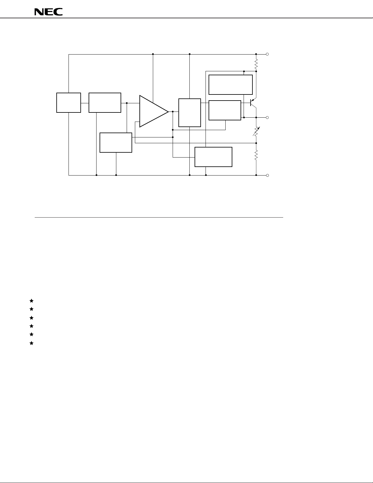
BLOCK DIAGRAM
Safe operating
area protection
µ
PC2900 Series
INPUT
Start-up
circuit
Reference
voltage
Thermal
shut down
Error
amp.
Drive
circuit
Saturation
protection
Over current
protection
ORDERING INFORMATION
Part Number Package Output Voltage
µ
PC2903HF MP-45G (Isolated TO-220) 3.0 V
µ
PC2903HB MP-3 (SC-64) 3.0 V
µ
PC2903T MP-3Z (SC-63) 3.0 V
µ
PC2933HF MP-45G (Isolated TO-220) 3.3 V
µ
PC2933HB MP-3 (SC-64) 3.3 V
µ
PC2933T MP-3Z (SC-63) 3.3 V
µ
PC2905HF MP-45G (Isolated TO-220) 5.0 V
µ
PC2905HB MP-3 (SC-64) 5.0 V
µ
PC2905T MP-3Z (SC-63) 5.0 V
µ
PC2906HF MP-45G (Isolated TO-220) 6.0 V
µ
PC2906HB MP-3 (SC-64) 6.0 V
µ
PC2906T MP-3Z (SC-63) 6.0 V
µ
PC2907HF MP-45G (Isolated TO-220) 7.0 V
µ
PC2907HB MP-3 (SC-64) 7.0 V
µ
PC2907T MP-3Z (SC-63) 7.0 V
µ
PC2908HF MP-45G (Isolated TO-220) 8.0 V
µ
PC2908HB MP-3 (SC-64) 8.0 V
µ
PC2908T MP-3Z (SC-63) 8.0 V
µ
PC2909HF MP-45G (Isolated TO-220) 9.0 V
µ
PC2909HB MP-3 (SC-64) 9.0 V
µ
PC2909T MP-3Z (SC-63) 9.0 V
µ
PC2910HF MP-45G (Isolated TO-220) 10.0 V
µ
PC2910HB MP-3 (SC-64) 10.0 V
µ
PC2910T MP3Z (SC-63) 10.0 V
µ
PC2912HF MP-45G (Isolated TO-220) 12.0 V
µ
PC2912HB MP-3 (SC-64) 12.0 V
µ
PC2912T MP-3Z (SC-63) 12.0 V
OUTPUT
GND
2

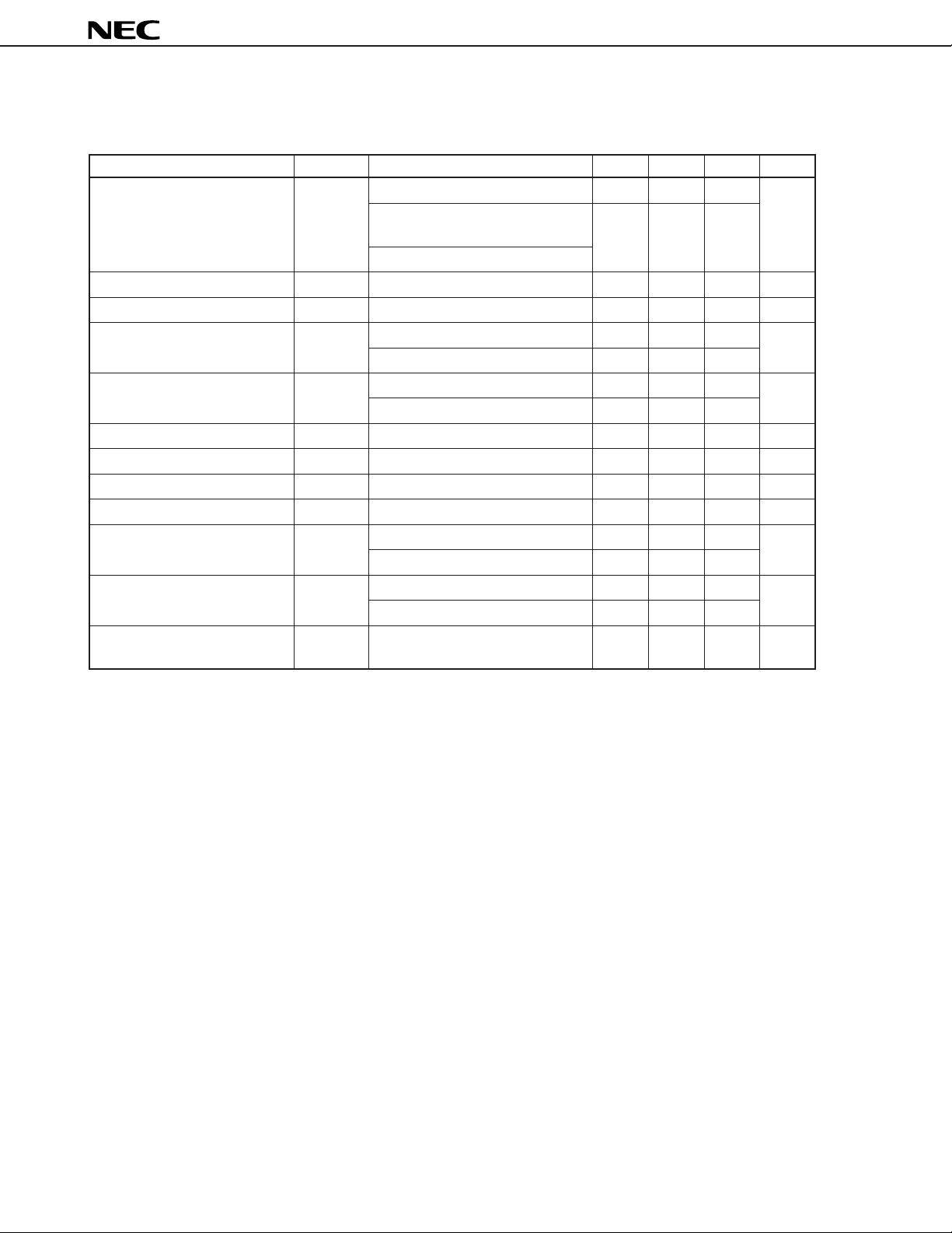
ABSOLUTE MAXIMUM RATINGS (TA = 25 °C, Unless otherwise specified.)
µ
PC2900 Series
Parameter Symbol
Input Voltage VIN 20 V
Internal Power Dissipation
Operating Ambient Temperature TA –30 to +85 °C
Operating Junction Temperature TJ –30 to +150 °C
Storage Temperature Tstg –55 to +150 °C
Thermal Resistance (Junction to Case) Rth (J-C) 7 12.5 °C/W
Thermal Resistance (Junction to Ambient)
Note
PT 15 10 W
Rth (J-A) 65 125 °C/W
µ
PC2900HF
Rating
µ
PC2900HB, µPC2900T
Note TC = 25 °C, Internally limited
When operating junction temperature rises up to 150 °C, the internal circuit shutdown output voltage.
Caution Exposure to Absolute Maximum Ratings for extended periods may affect device reliability;
exceeding the ratings could cause permanent damage. The parameters apply independently. The
device should be operated within the limits specified under DC and AC Characteristics.
TYPICAL CONNECTION
D
1
Unit
PC2900
INPUT
C
IN
µ
+
OUT
C
D
OUTPUT
2
CIN : More than 0.1 µF. Required if regulator is located an appreciable distance from power supply filter. You
must use to prevent from the parasitic oscillation.
OUT : More than 47
C
µ
F. You must use the Low-impedance-type (low ESR) capacitor.
D1 : Need for VO > VIN
D2 : Need a shottky barrier diode for VO < GND.
3

µ
PC2900 Series
RECOMMENDED OPERATING CONDITIONS
Parameter Symbol Type Number MIN. TYP. MAX. Unit
Input Voltage VIN
Output Current IO all 0 1.0 A
Operating Ambient Temperature TA all –30 +85 °C
Operating Junction Temperature TJ all –30 +125 °C
µ
PC2903 4.0 16 V
µ
PC2933 4.3 16
µ
PC2905 6 16
µ
PC2906 7 16
µ
PC2907 8 16
µ
PC2908 9 18
µ
PC2909 10 18
µ
PC2910 11 18
µ
PC2912 13 18
ELECTRICAL CHARACTERISTICS µPC2903 (TJ = 25 °C, VIN = 5 V, IO = 500 mA, CIN = 0.22 µF, COUT = 47 µF,
unless otherwise specified.)
Parameters Symbol Conditions MIN. TYP. MAX. Unit
Output Voltage VO 2.88 3.0 3.12 V
0 °C ≤ TJ ≤ 125 °C, 4.0 V ≤ VIN ≤ 16 V,
0 A ≤ IO ≤ 500 mA
0 °C ≤ TJ ≤ 125 °C, 0 A ≤ IO ≤ 1 A
Line Regulation REGIN 4.0 V ≤ VIN ≤ 16 V 11 30 mV
Load Regulation REGL 0 A ≤ IO ≤ 1 A 9 30 mV
Quiescent Current IBIAS IO = 0 A 1.9 4.0 mA
IO = 1 A 23 60
Startup Quiescent Current IBIAS (s) VIN = 2.95 V, IO = 0 A 12 30 mA
VIN = 2.95 V, IO = 1 A 80
Quiescent Current Change ∆IBIAS
Output Noise Voltage Vn 10 Hz ≤ f ≤ 100 kHz 52
Ripple Rejection R·R f = 120 Hz, 4.0 V ≤ VIN ≤ 16 V 48 63 dB
Dropout Voltage VDIF 0 °C ≤ TJ ≤ 125 °C, IO = 1 A 0.7 1.0 V
Short Circuit Current IO short VIN = 4.5 V 1.2 1.7 3.0 A
Peak Output Current IO peak VIN = 4.5 V 1.0 1.5 3.0 A
Temperature Coefficient of ∆VO/∆T0 °C ≤ TJ ≤ 125 °C, IO = 5 mA –0.5 mV/°C
Output Voltage
0 °C ≤ TJ ≤ 125 °C, 4.0 V ≤ VIN ≤ 16 V
VIN = 16 V 1.2
VIN = 16 V 1.3 1.7 2.8
2.85 3.15
3.2 20 mA
µ
Vr.m.s.
4

µ
PC2900 Series
ELECTRICAL CHARACTERISTICS µPC2933 (TJ = 25 °C, VIN = 5 V, IO = 500 mA, CIN = 0.22 µF, COUT = 47 µF,
unless otherwise specified.)
Parameters Symbol Conditions MIN. TYP. MAX. Unit
Output Voltage VO 3.17 3.3 3.43 V
0 °C ≤ TJ ≤ 125 °C, 4.3 V ≤ VIN ≤ 16 V,
0 A ≤ IO ≤ 500 mA
0 °C ≤ TJ ≤ 125 °C, 0 A ≤ IO ≤ 1 A
Line Regulation REGIN 4.3 V ≤ VIN ≤ 16 V 12 33 mV
Load Regulation REGL 0 A ≤ IO ≤ 1 A 23 33 mV
Quiescent Current IBIAS IO = 0 A 2.0 4.0 mA
IO = 1 A 30 60
Startup Quiescent Current IBIAS (s) VIN = 3.1 V, IO = 0 A 10 30 mA
VIN = 3.1 V, IO = 1 A 80
Quiescent Current Change ∆IBIAS
Output Noise Voltage Vn 10 Hz ≤ f ≤ 100 kHz 55
Ripple Rejection R·R f = 120 Hz, 4.3 V ≤ VIN ≤ 16 V 48 64 dB
Dropout Voltage VDIF 0 °C ≤ TJ ≤ 125 °C, IO = 1 A 0.7 1.0 V
Short Circuit Current IO short VIN = 4.5 V 1.2 1.6 3.0 A
Peak Output Current IO peak VIN = 4.5 V 1.0 1.4 3.0 A
Temperature Coefficient of ∆VO/∆T0 °C ≤ TJ ≤ 125 °C, IO = 5 mA –0.4 mV/°C
Output Voltage
0 °C ≤ TJ ≤ 125 °C, 4.3 V ≤ VIN ≤ 16 V
VIN = 16 V 1.2
VIN = 16 V 1.3 1.7 2.8
3.14 3.46
3.0 20 mA
µ
Vr.m.s.
5
µ
PC2900 Series
ELECTRICAL CHARACTERISTICS µPC2905 (TJ = 25 °C, VIN = 8 V, IO = 500 mA, CIN = 0.22 µF, COUT = 47 µF,
unless otherwise specified.)
Parameters Symbol Conditions MIN. TYP. MAX. Unit
Output Voltage VO 4.8 5.0 5.2 V
0 °C ≤ TJ ≤ 125 °C, 6 V ≤ VIN ≤ 16 V,
0 A ≤ IO ≤ 500 mA
0 °C ≤ TJ ≤ 125 °C, 0 A ≤ IO ≤ 1 A
Line Regulation REGIN 6 V ≤ VIN ≤ 16 V 23 50 mV
Load Regulation REGL 0 A ≤ IO ≤ 1 A 28 50 mV
Quiescent Current IBIAS IO = 0 A 2.2 4.0 mA
IO = 1 A 30 60
Startup Quiescent Current IBIAS (s) VIN = 4.5 V, IO = 0 A 10 30 mA
VIN = 4.5 V, IO = 1 A 80
Quiescent Current Change ∆IBIAS
Output Noise Voltage Vn 10 Hz ≤ f ≤ 100 kHz 90
Ripple Rejection R·R f = 120 Hz, 6 V ≤ VIN ≤ 16 V 46 61 dB
Dropout Voltage VDIF 0 °C ≤ TJ ≤ 125 °C, IO = 1 A 0.7 1.0 V
Short Circuit Current IO short VIN = 6.5 V 1.15 1.8 3.0 A
Peak Output Current IO peak VIN = 6.5 V 1.1 1.5 3.0 A
Temperature Coefficient of ∆VO/∆T0 °C ≤ TJ ≤ 125 °C, IO = 5 mA 0.6 mV/°C
Output Voltage
0 °C ≤ TJ ≤ 125 °C, 6 V ≤ VIN ≤ 16 V
VIN = 16 V 1.1
VIN = 16 V 1.4 2.0 2.8
4.75 5.25
2.9 20 mA
µ
Vr.m.s.
6
 Loading...