


NEC UPD75116GF-XXX-3BE, UPD75116GF-A-XXX-3BE, UPD75116CW-XXX, UPD75116CW-A-XXX, UPD75112GF-A-XXX-3BE Datasheet
...
Description
The µPD75116(A) is one of the 4-bit single-chip microcomputer 75X series.
The µPD75116(A) is a product with the extended ROM
capacity of the µPD75108(A). In addition of high-speed
operations, it can manipulate data in units of 1, 4 and 8
bits. In particular, the I/O operation of the µPD75116
have been improved by a wide variety of bit control
instructions. The µPD75116 is provided with interface
inputs/outputs with peripheral circuits having different
power voltages, and analog inputs and suitable for
controlling automobile electrical equipment, etc. For
the µPD75116(A), an on-chip pin-compatible one-time
PROM product (µPD75P116) is separately available for
system development evaluation.
Functions are described in detail in the following User’s
Manual, which should be read when carrying out
design work.
µ
PD751×× Series User’s Manual: IEM-992
Features
• Higher reliability than µPD75116
• Architecture "75X" equivalent to 8-bit microcomputer
• Minimum instruction execution time (high-speed
operation): 0.95 µs (when operated at 4.19 MHz and
5 V)
• Instruction execution variable function: 0.95µs/1.91µs/
15.3 µs (when operated at 4.19 MHz)
• Many input/output ports: 58
• 3-channel on-chip 8-bit timers
• 8-bit on-chip serial interface
• Multi-interruptible vector interrupt function
Applications
Automobile electrical equipment, etc.
Data Sheet
µ
PD75112(A), 75116(A)
4-Bit Single Chip-Microcomputer
©NEC Corporation 1990
Qualty Grade
Special
Special
Special
Special
Package
64-pin plastic shrink DIP
(750 mil)
64-pin plastic QFP
(14 × 20 mm)
64-pin plastic shrink DIP
(750 mil)
64-pin plastic QFP
(14 × 20 mm)
Ordering Code
µ
PD75112CW(A)-×××
µ
PD75112GF(A)-×××-3BE
µ
PD75116CW(A)-×××
µ
PD75116GF(A)-×××-3BE
Remarks: ××× is a ROM code number.
Please refer to "Quality Grade on NEC Semiconductor Devices" (Document number IEI-1209) published by NEC Corporation to know the specification of quality grade on the devices and its recommended applications.
Unless there are any particular functional differences,
the µPD75116(A) is described in this document as a
representative product.
The information in this document is subject to change without notice.
The mark ★ shows major revised points.
Document No. IC-2811A
(O. D. No. IC-8261A)
Date Published March 1994 P
Printed in Japan

2
µ
PD75112(A), 75116(A)
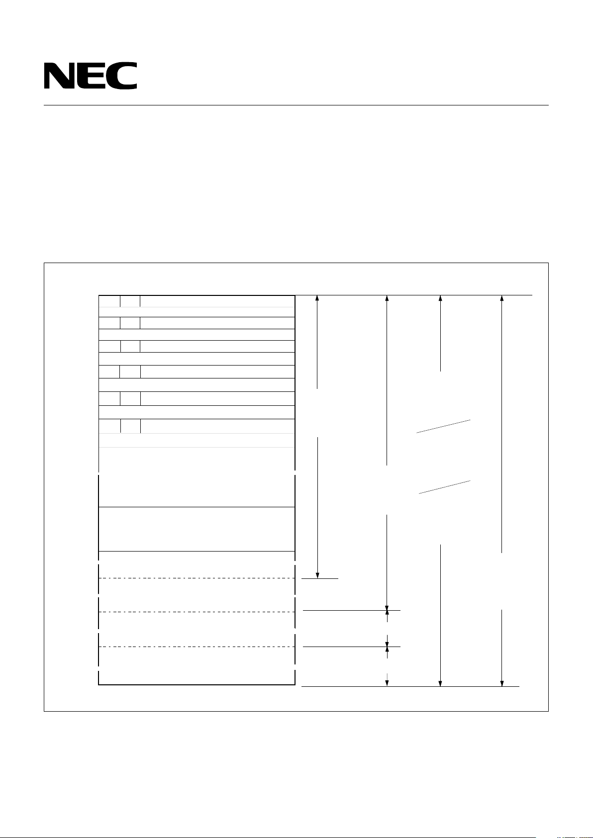
Item
No. of basic instruction
Min. instruction execution time
On-chip memory
General register
Accumulator
Input/output port
Timer/counter
Serial interface
Vector interrupt
Test input
Standby
Operating temperature range
Operating voltage
Others
Package
Description
43
0.95 µs/1.91 µs/15.3 µs (when operated at 4.19 MHz), switchable at 3 levels
12160 × 8 (µPD75112(A)), 16256 × 8 (µPD75116(A))
512 × 4
4 bits × 8 × 4 banks (memory mapping)
Three accumulated in compliance with controlled date lengths
•1-bit accumulator (CY), 4-bit accumulator (A), 8-bit accumulator (XA)
58 in total
• CMOS input pin : 10
• CMOS input/output pin (LED direct drive enable) : 32
• Intermediate withstand voltage N-ch open drain : 12
input/output pin (bit-wise pull-up resistor inscorporation possible)
• Comparator input pin (4-bit accuracy) : 4
• 8-bit timer/event counter × 2
• 8-bit basic interval timer (applicable to watchdog timer)
• 8-bits
• First LSB/first MSB switchable
• Two transfer modes (transmit and receiver/receive dedicated mode)
External : 3, Internal : 4
External : 2
• STOP/HALT mode
-40 to +85°C
2.7 to 6.0 V
• On-chip power-on reset circuit (mask option)
• On-chip bit contol memory (bit sequential buffer)
• 64-pin plastic shrink DIP (750 mil)
• 64-pin plastic QFP (14 × 20 mm)
Defferences between µPD75112(A), 75116(A) and µPD75112, 75116
Item
Quality grade
Electrical specifications
Direct LED drive
Outline of Functions
ROM
RAM
Absolute maximum ratings
DC characteristics
µ
PD75112(A), 75116(A)
Special
Different high-level output current and low-level output current
Different low-level output voltage
Not possible
Product Name
µ
PD75112, 75116
Standard
Possible

3
µ
PD75112(A), 75116(A)
CONTENTS
1. Pin Configuration (Top View)............................................................................................... 4
2. Block Diagram......................................................................................................................... 6
3. Pin Functions......................................................................................................................... 7
3.1 Port Pins...................................................................................................................................................... 7
3.2 Non-Port Pins............................................................................................................................................... 8
3.3 Pin Input/Output Circuits............................................................................................................................ 9
3.4 Recommended Connection of Unused Pins............................................................................................. 10
3.5 Caution Relating to Use of P00/INT4 Pin and RESET Pin........................................................................ 10
4. Memory Configuration............................................................................................................. 11
5. Peripheral Hardware Functions.............................................................................................. 14
5.1 Digital Input/Output Port......................................................................................................................... 14
5.2 Clock Generator......................................................................................................................................... 14
5.3 Clock Output Circuit.................................................................................................................................. 16
5.4 Basic Interval Timer.................................................................................................................................... 16
5.5 Timer/Event Counter................................................................................................................................. 17
5.6 Serial Interface............................................................................................................................................ 19
5.7 Programmable Threshold Port (Analog Input Port)............................................................................... 21
5.8 Bit Sequential Buffer................................................................................................................................... 22
5.9 Power-On Flag (Mask Option).................................................................................................................... 22
6. Interrupt Functions.................................................................................................................. 23
7. Standby Functions ............................................................................................................... 25
8. Reset Functions..................................................................................................................... 26
9. Instruction Set....................................................................................................................... 29
10. Mask Option Selection.......................................................................................................... 37
11. Electrical Specifications........................................................................................................ 38
12. Package Information ............................................................................................................ 48
13. Recommended Soldering Conditions ................................................................................. 51
APPENDIX A. Diffeences between µPD751××(A) Series Products
and Related PROM Products.............................................................................. 52
APPENDIX B. Development Tools ............................................................................................ 53
APPENDIX C. Related Documentations ................................................................................... 54
4
µ
PD75112(A), 75116(A)
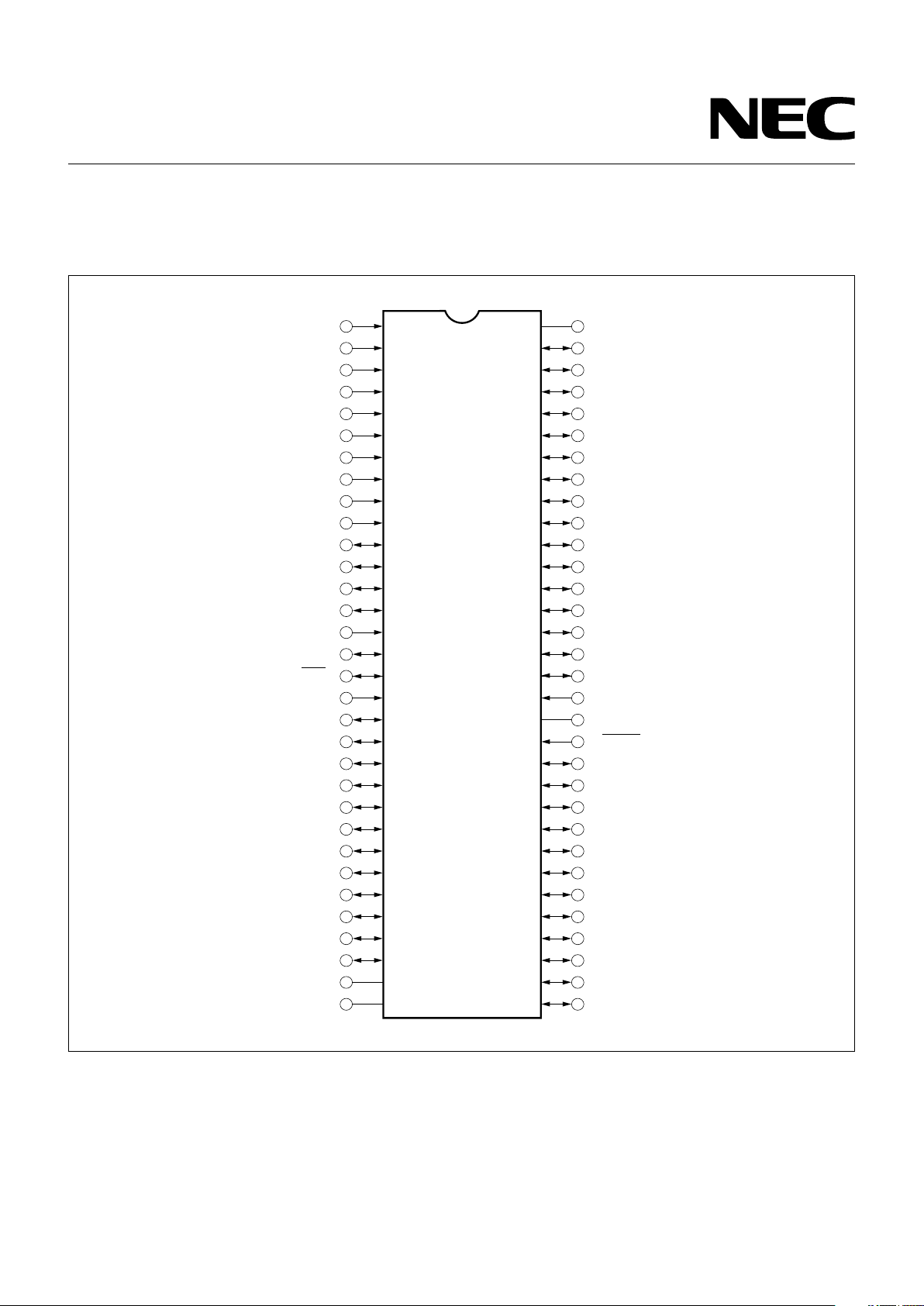
1. Pin Configuration (Top View)
64-Pin Plastic Shrink DIP (750 mil)
1
P13/INT3
2
P12/INT2
3
P11/INT1
4
P10/INT0
5
PTH03
6
PTH02
7
PTH01
8
PTH00
9
TI0
10
TI1
11
P23
12
P22/PCL
13
P21/PTO1
14
P20/PTO0
15
P03/SI
16
P02/SO
17
P01/SCK
18
P00/INT4
19
P123
20
P122
21
P121
22
P120
23
P133
24
P132
25
P131
26
P130
27
P143
28
P142
29
P141
30
P140
31
NC
32
V
DD
64
63
62
61
60
59
58
57
56
55
54
53
52
51
50
49
48
47
46
45
44
43
42
41
40
39
38
37
36
35
34
33
V
SS
P90
P91
P92
P93
P80
P81
P82
P83
P70
P71
P72
P73
P60
P61
P62
P63
X1
X2
RESET
P50
P51
P52
P53
P40
P41
P42
P43
P30
P31
P32
P33
µ
PD75112CW(A)-×××
µ
PD75116CW(A)-×××

5
µ
PD75112(A), 75116(A)
1
2
3
4
5
6
7
8
9
10
11
12
13
14
15
16
P131
P132
P133
P120
P121
P122
P123
P00/INT4
P02/SO
P01/SCK
P03/SI
P20/PTO0
P21/PTO1
P22/PCL
P23
T11
X2
X1
P41
P40
P53
P52
P51
P50
RESET
P63
P62
P61
P60
P73
P72
P71
20 21 22 23 24 25 26 27 28 29 30 31 32
64 63 62 61 60 59 58 57 56 55 54 53 52
51
50
49
48
47
46
45
44
43
42
41
40
39
38
37
36
P42
P43
P30
P31
P32
P33
VDDNC
P140
P141
P142
P143
P130
P81
P80
P93
P92
P91
P90
V
SS
P13/INT3
P12/INT2
P11/INT1
P10/INT0
PTH03
PTH02
17
18
19
P70
P83
P82
T10
PTH00
PTH01
35
34
33
64-Pin Plastic QFP (14 × 20 mm)
µ
PD75112GF(A)-×××-3BE
µ
PD75116GF(A)-×××-3BE
Pin Name
P00-P03 : Port0 SCK : Serial Clock
P10-P13 : Port1 SO : Serial Output
P20-P23 : Port2 SI : Serial Input
P30-P33 : Port3 PTO0, PTO1 : Programmable Timer Output
P40-P43 : Port4 PCL : Programmable Clock
P50-P53 : Port5 PTH00-PTH03 : Programmable Threshold Input
P60-P63 : Port6 INT0, INT1, INT4 : External Vectored Interrupt Input
P70-P73 : Port7 INT2, INT3 : External Test Input
P80-P83 : Port8 TI0, TI1 : Timer Input
P90-P93 : Port9 X1, X2 : Clock Oscillation
P120-P123 : Port12 RESET : Reset
P130-P133 : Port13 NC : No Connection
P140-P143 : Port14 VDD : Positive Power Supply
VSS : Ground
★

6
µ
PD75112(A), 75116(A)
2. Block Diagram
ROM
PROGRAM
MEMORY
12160 × 8 BITS
( PD75112(A))
16256 × 8 BITS
( PD75116(A))
µ
P00-P03
P10-P13
PORT0
PORT1 4
P20-P23
4
P30-P33
4
P40-P43
4
P50-P53
4
P60-P63
4
P70-P73
4
P80-P83
4
P90-P93
4
P120-P123
4
P130-P133
4
P140-P143
4
4
BIT SEQ.
BUFFER(16)
PORT2
PORT4
PORT3
PORT5
PORT6
PORT7
PORT8
PORT9
PORT12
PORT13
PORT14
GENERAL REG.
BANK
SP (8)CY
ALU
RAM
DATA MEMORY
512 × 4 BIT
DECODE
AND
CONTROL
TIMER/EVENT
COUNTER
# 0
TIMER/EVENT
COUNTER
# 1
SERIAL
INTERFACE
CLOCK
OUTPUT
CONTROL
CLOCK
DIVIDER
CLOCK
GENERATOR
STAND BY
CONTROL
CPU CLOCK
PCL/P22
f
X
/2
X1 X2
RESET
V
SS
V
DD
BASIC
INTERVAL
TIMER
INTBT
TI0
PTO0/P20
TI1
PTO1/P21
SI/P03
SI/P02
INT0/P10
INT1/P11
INT2/P12
INT3/P13
INT4/P00
4
PTH00-PTH03
SCK/P01
INTT0
INTT1
INTSIO
INTERRUPT
CONTROL
PROGRAMMABLE
THRESHOLD
PORT # 0
PROGRAM
COUNTER (14)
µ
N
Φ

7
µ
PD75112(A), 75116(A)
3. Pin Functions
3.1 Port Pins
Pin Name
P00
P01
P02
P03
P10
P11
P12
P13
P20
P21
P22
P23
P30 to P33
P40 to P43
P50 to P53
P60 to P63
P70 to P73
P80 to P83
P90 to P93
P120 to P123
P130 to P133
P140 to P143
Function
4-bit input port (PORT0)
4-bit input port (PORT1)
4-bit input/output port (PORT2)
Programmable 4-bit input/output port (PORT3)
Bit-wise input/output setting enable
4-bit input/output port (PORT4)
4-bit input/output port (PORT5)
Programmable 4-bit input/output port (PORT6)
Bit-wise input/output setting enable
4-bit input/output port (PORT7)
4-bit input/output port (PORT8)
4-bit input/output port (PORT9)
N-ch open drain 4-bit input/ output port (PORT12)
Bit-wise pull-up resistor incorporation enable
(mask option)
2 V withstand for open drain
N-ch open drain 4-bit input/ output port (PORT13)
Bit-wise pull-up resistor incorporation enable
(mask option)
12 V withstand for open drain
N-ch open drain 4-bit input/output port (PORT14)
Bit-wise pull-up resistor incorporation enable
(mask option)
12 V withstand for open drain
I/O Circuit
Type *1
B
F
E
B
B
E
E
E
E
E
E
E
E
M
M
M
Input/ Output
Input
Input/output
Input/output
Input
Input
Input/output
Input/output
Input/output
Input/output
Input/output
Input/output
Input/output
Input/output
Input/output
Input/output
Input/output
8-Bit I/O
×
×
●●
●●
●●
●●
At Reset
Input
Input
Input
Input
Input
Input
Input
Input
Input
Input
Input*2
Input*2
Input*2
* 1: Circles indicate Schmitt trigger inputs.
2: High impedance for open drain
High level for on-chip pull-up resistors
Dual
Function Pin
INT4
SCK
SO
SI
INT0
INT1
INT2
INT3
PTO0
PTO1
PCL

8
µ
PD75112(A), 75116(A)
PTH00 to PTH03
TI0
TI1
PTO0
PTO1
SCK
SO
SI
INT4
INT0
INT1
INT2
INT3
PCL
X1, X2
RESET
NC*2
VDD
VSS
3.2 Non-Port Pins
Dual
Function
Pin
P20
P21
P01
P02
P03
P00
P10
P11
P12
P13
P22
I/O
Circuit
Type*1
N
B
E
F
E
B
B
B
B
E
B
At Reset
Input
Input
Input
Input
Input
Input
Input
Input
Input/Output
Input
Input
Input/output
Input/output
Input/output
Input
Input
Input
Input
Input/output
Input
Function
Threshold voltage ariable 4-bit analogy input port.
External event pulse input for the timer/event counter or edge
detect vector interrupt input. 1-bit input enable.
Timer/event counter output.
Serial clock input/output.
Serial data output.
Serial data input.
Edge detect vector interrupt input (for detecting both rising and
falling edges).
Edge detect vector interrupt input (detected edge selectable).
Edge detect testable input (for rising edge detection).
Clock output.
Crystal/ceramic connect pin (system clock oscillation).
In case with the external clock, input a signal to X1 and the
antiphase to X2.
System reset input (low level active).
No Connection
Positive power supply.
GND potential.
*1: Circles indicate Schmitt trigger inputs.
2: When the PWB is shared with the µPD75P116, connect the NC pin to VDD directly.

9
µ
PD75112(A), 75116(A)
Type F
Input/output circuit consisting of a Type D push-pull output
and a Type B Schmitt-triggered input.
Type M
Pull-Up Register (Mask Option)
N-ch (+6 V
Withstand)
Middle-High Voltage Input Buffer (+6 V Withstand)
Type N
Comparator
VREF (Threshold Voltage)
3.3 Pin Input/Output Circuits
µ
PD75116(A) pin input/output crcuit are shown in sche-
matic form.
Figure 3-1 Pin Input/Output Circuits
IN/OUT
data
output
disable
Type D
Type B
P-ch
V
DD
IN
N-ch
IN
+
–
IN
P-ch
V
DD
OUT
N-ch
data
output
disable
IN/OUT
data
output
disable
Type D
Type A
IN/OUT
V
DD
data
output
disable
Type A
CMOS specified input buffer
Type B
Schmitt triggered-input with hysteresis characteristics
Type D
Push-pull output which can be set at output high impedance
(with both P-ch an N-ch set to OFF)
Type E
Input/output circuit consisting of a Type D push-pull output
and a Type A input buffer

10
µ
PD75112(A), 75116(A)
3.5 Caution Relating to Use of P00/INT4 Pin and RESET Pin
In addition to the functions described in sections 3.1
and 3.2, the P00/INT4 pin and the RESET pin have the
function to set the IC test mode for testing the
µ
PD75116(A) internal operations.
When a voltage larger than VDD is applied to one of
these two pins, the test mode is set. Thus, if noise
exceeding VDD is applied even during normal operations, the test mode is set and normal operations may
be discontinued.
For example, if a cable from the P00/INT4 or RESET pin
is too long, inter-wiring noise may be applied to the pin,
the pin voltage may become larger than VDD, causing
malfunctioning.
Thus, carry out wiring to minimize inter-wiring noise. If
the noise cannot be suppressed completely, carry out
the following countermeasure against noise using an
externally mounted component.
o Connect a diode with low VF (max 0.3 V)between VDDs
Diode with low VF
o Connect acapacitor between VDDs
3.4 Recommended Connection of Unused Pins
Pin
PTH00 to PTH03
TI0
TI1
P00
P01 to P03
P10 to P13
P20 to P23
P30 to P33
P40 to P43
P50 to P53
P60 to P63
P70 to P73
P80 to P83
P90 to P93
P120 to P123
P130 to P133
P140 to P143
RESET
NC
*1: Only when a power-on reset generator is built in by mask
option, connect t VDD.
2: When the PWB is shared with the µPD75P116, connect the
NC pin to VDD directly.
Recommended Connecting Method
Connect to VSS or VDD
Connect to VSS
Connect to VSS or VDD
Connect to VSS
Input state : Connect to VSS or VDD
Output state : Leave open
Connect to VDD*1
Leave open or connect to VDD*2
V
DD
V
DD
P00/INT4, RESET
V
DD
V
DD
P00/INT4, RESET
11
µ
PD75112(A), 75116(A)
4. Memory Configuration
• Program Memory (ROM)
12160 × 8 bits (0000H to 2F7FH): µPD75112(A)
16256 × 8 bits (0000H to 3F7FH):µPD75116(A)
• 0000H to 0001H: Vector table for writing the
program start address by reset
• 0002H to 000BH: Vector table for writing the
program start address by interrupt
Remarks: In all other cases, the program can be
branched by the BR PCDE and BR PCXA
• 0020H to 007FH: Table area to be referred to
by the GETI instruction
• Data Memory
• Data area
512 × 4 bits (000H to 1FFH)
• Peripheral hardware area
128 × 4 bits (F80H to FFFH)
instructions to an address with only the
lower 8 bits of PC changed.
Figure 4-1 Program Memory Map (µPD75112(A))
Address
≈
≈
≈
MBE RBE
MBE
RBE
MBE
MBE RBE
MBE
RBE
MBE
RBE
0000H
0002H
0004H
0006H
0008H
000AH
0020H
007FH
0080H
07FFH
0FFFH
76
0
Internal Reset Start Address
Internal Reset Start Address
(Low-Order 8 Bits)
INT0/INT1 Start Address (High-Order 6 Bits)
INT0/INT1 Start Address
(Low-Order 8 Bits)
(Low-Order 8 Bits)
INTSIO Start Address (High-Order 6 Bits)
INTSIO Start Address
(Low-Order 8 Bits)
INTT0 Start Address (High-Order 6 Bits)
INTT0 Start Address
(Low-Order 8 Bits)
INTT1 Start Address (High-Order 6 Bits)
INTT1 Start Address
GETI Instruction Reference Table
CALLF
! faddr
Instruction
Entry
Address
BRCB
! caddr
Instruction
Branch
Address
BR !addr
Instruction
Branch
Address
CALL !addr
Instruction
Subroutin
Entry
Address
BRCB !caddr Instruction
Branch Address
≈
(High-Order 6 Bits)
RBE
INTBT/INT4 Start Address (High-Order 6 Bits)
INTBT/INT4 Start Address
(Low-Order 8 Bits)
≈
≈
≈
≈
≈
≈
2000H
1FFFH
2F7FH
0800H
1000H
BRCB !caddr Instruction
Branch Address
BR $addr
Instruction
Relative
Branch Address
(-15 to +16)
Branch Address
Subroutine Entry
Address by GETI
Instruction

12
µ
PD75112(A), 75116(A)
Figure 4-2 Program Memory Map (µPD75116(A))
Address
Remarks: In all other cases, the program can be
branched by the BR PCDE and BR PCXA
instructions to an address with only the lower
8 bits of PC changed.
≈
≈
≈
MBE RBE
MBE
RBE
MBE
MBE RBE
MBE
RBE
MBE
RBE
0000H
0002H
0004H
0006H
0008H
000AH
0020H
007FH
0080H
07FFH
0FFFH
76
0
Internal Reset Start Address
Internal Reset Start Address
(Low-Order 8 Bits)
INT0/INT1 Start Address (High-Order 6 Bits)
INT0/INT1 Start Address
(Low-Order 8 Bits)
(Low-Order 8 Bits)
INTSIO Start Address (High-Order 6 Bits)
INTSIO Start Address
(Low-Order 8 Bits)
INTT0 Start Address (High-Order 6 Bits)
INTT0 Start Address (High-Order 6 Bits)
INTT1 Start Address (High-Order 6 Bits)
INTT1 Start Address
GETI Instruction Reference Table
CALLF
! faddr
Instruction
Entry
Address
BRCB
! caddr
Instruction
Branch
Address
BR !addr
Instruction
Branch
Address
CALL !addr
Instruction
Subroutin
Entry
Address
BRCB !caddr Instrucion
Branch Address
≈
(High-Order 6 Bits)
RBE
INTBT/INT4 Start Address (High-Order 6 Bits)
INTBT/INT4 Start Address
(Low-Order 8 Bits)
≈
≈
≈
≈
≈
≈
≈
≈
2000H
1FFFH
3000H
2FFFH
3F7FH
0800H
1000H
BRCB !caddr Instruction
Branch Address
BR $addr
Instruction
Relative
Branch Address
(-15 to –1
+2 to +16)
BRCB !caddr Instrucion
Branch Address
Branch Address
Subroutine Entry
Address by GETI
Instruction

13
µ
PD75112(A), 75116(A)
Figure 4-3 Data Memory Map
Memory Bank
Data Memory
000H
01FH
0FFH
100H
1FFH
F80H
FFFH
Bank 0
Bank 1
Bank 15
256 × 4
128 × 4
256 × 4
(32 × 4)
General
Regoster Area
Stack Area
Data Area
Static RAM
(512 × 4)
Peripheral Hardware
Area
Not Incorporated

14
µ
PD75112(A), 75116(A)
Table 5-1 Functions of Digital Ports
Remarks
Share the pins with SI, SO, SCK and
INT0 to 4.
Port 2 shares the pin with PTO0,
PTO1 and PCL.
On-chip pull-up registers can be
specified bit-wise by mask option.
5. Peripheral Hardware Functions
5.1 Digital Input/Output Port
The digital input/output port has the following tree types.
• CMOS input (PORT0, 1) : 8
• CMOS input/output (PORT 2 to PORT 9) : 32
• N-ch open-drain input/output (PORT 12 to PORT 14): 12
Total 52
Functions
4-bit input
4-bit input/
output
4-bit input/
output
(N-ch opendrain, 12 V
withstand
voltage)
Port (Code)
PORT0
PORT1
PORT3
PORT6
PORT2
PORT4
PORT5
PORT7
PORT8
PORT9
PORT12
PORT13
PORT14
Operations and Features
Read or test always enable irrespectively of the operating mode
of dual-function pins.
Can be set bit-wise to the input or output mode.
Can be set in 4-bit units to the input or output mode.
Ports 4 and 5, 6 and 7, 8 and 9 can form pairs and data can be
input/output in 8-bit units.
Can be set in 4-bit units the input or output mode.
Ports 12 and 13 can form a pair and data can be input/output in 8bit units.
5.2 Clock Generator
The clock generator is a circuit which supplies the CPU
and peripheral hardware with various clocks and controls the CPU operating mode.
The instruction execution time can be changed.
• 0.95 µs/1.91 µs/15.3 µs (at 4.19 MHz operation)

15
µ
PD75112(A), 75116(A)
Figure 5-1 Block Diagram of Clock Generator
• Basic Interval Timer (BT)
• Clock Generator
• Timer/Event Counter
• Serial Interface
• Clock Output Circuit
S
RQ
1/4
S
STOP F/F
HALT F/F
Q
R
1/2 1/16
1/8 to 1/4096
PCC
fx
fxx or
PCC0
PCC1
PCC2
PCC3
PCC2,
PCC3
Crear
STOP*
HALT*
4
Φ
• CPU
• Clock Output Circuit
Inter-
nal
Bus
System
Clock
Oscillator
Oscillation Stop
Frequency Divider
Selec-
tor
Frequency
Divider
Wait Release Signal from BT
RES(Internal Reset) Signal
Standby Release Signal from
the Interrupt Control Circuit
Remarks 1:fXX=crystal/ceramic oscillator frequency.
2:fX=external clock frequency.
3:Φ=CPU clock
4: *indicates instruction execution.
5: PCC (processor clock control register)
6: 1 clock cycle (tCY) of Φ is 1 michine cycle of the instruc-
tion. For tCY, see the AC characteristics in the 11."Electrical Specifications".
★

16
µ
PD75112(A), 75116(A)
5.4 Basic Interval Timer
The basic interval timer has the following functions;
• Interval timer operation to generate reference
time interrupts
• Watchdog timer application to detect program
overrun
• Wait time selection and count when the standby
mode is released
• Count content read
5.3 Clock Output Circuit
The clock output circuit is a circuit to generate clock
pulses from the P22/PCL pin. It is used to supply the
peripheral LSIs with clock pulses.
•Clock output (PCL):Φ, 524 kHz, 262 kHz (at 4.19 MHz
operation)
The clock output cicuit configuration is shown as the
following.
Figure 5-2 Clock Output Circuit Configuration
PORT2.2
CLOM3 CLOM1 CLOM0
fxx/2
CLOM0
4
3
fxx/2
4
Φ
From the Clock
Generator
Selector
Internal Bus
P22
Output Latch
Port 2 Input/
Output Mode
Specification Bit
PMGB Bit 2
P22/PCL
Output Buffer

17
µ
PD75112(A), 75116(A)
Figure 5-3 Basic Interval Timer Configuration
Remark: * indicates instruction execution.
5.5 Timer/Event Counter
The µPD75116(A) has a two-channel on-chip timer/
event counters.
Channels 0 and 1 of the timer/event counter have the
same configuration and functions. They differ only in
the selectable count pulse (CP) and the function of
supplying clocks to the serial interface.
The timer/event counter has the following functions:
• Programmable interval timer operation
• Output of square wave having any selected fre-
quency to PTOn pin
• Event counter operation
• Use of TIn pin as an external interrupt input pin
• Output of TIn pin input divided by N to PTOn pin
(frequency divider operation)
• Serial shift clock supply to the serial interface
circuit (channel 0 only)
• Count status read function
BTM3 BTM2 BTM1 BTM0
BTM
From
the Clock
Generator
*SET1
fxx/2
4
3
9
fxx/2
7
fxx/2
5
fxx/2
MPX
12
3
8
IRQBTBT
Internal Bus
Basic Interval Timer
(8-Bit Frequency Divider)
ClearClear
Wait Release Signal
When the Standby Mode
is Released
BT Interrupt
Request Flag
Vector
Interrupt
Request
Signal
Set
 Loading...