


NEC UPC2771TB-E3, UPC2771TB, UPC2771T-E3, UPC2771T, UPC2763TB-E3 Datasheet
...
DATA SHEET
BIPOLAR ANALOG INTEGRATED CI RCUITS
µµµµ
PC2762TB,
3 V, SUPER MINIMOLD SILICON MMIC
MEDIUM OUTPUT POWER AMPLIFIER
FOR MOBILE COMMUNICATIONS
DESCRIPTION
The
PC2762TB, µPC2763TB and µPC2771TB are silicon monolithic integrated circuits designed as amplifier for
µ
mobile communications. Each of the ICs is packaged in super minimold package which is smaller than conventional
minimold. The µPC2762TB, µPC2763TB and µPC2771TB have compatible pin connections and performance to
PC2762T, µPC2763T and µPC2771T of conventional minimold version. So, in the case of reducing your system
µ
size, µPC2762TB, µPC2763TB and µPC2771TB are suitable to replace from µPC2762T, µPC2763T and µPC2771T.
These IC is manufactured using NEC’s 20 GHz fT NESAT™III silicon bipolar process. This process uses silicon
nitride passivation film and gold electrodes. These materials can protect chip surface from external pollution and
prevent corrosion/migration. Thus, this IC has excellent performance, uniformity and reliability.
µµµµ
PC2763TB,
µµµµ
PC2771TB
FEATURES
• High-density surface mounting: 6-pin super minimold package (2.0 × 1.25 × 0.9 mm)
• Supply voltage : VCC = 2.7 to 3.3 V
• Medium output power :µPC2762TB: P
PC2763TB: P
µ
PC2771TB: P
µ
• Power gain :µPC2762TB: GP = 13 dB TYP. @ 0.9 GHz
PC2763TB: GP = 20 dB TYP. @ 0.9 GHz
µ
PC2771TB: GP = 21 dB TYP. @ 0.9 GHz
µ
APPLICATIONS
• Buffer amplifiers for mobile telephones: µPC2762TB, µPC2763TB
• PA driver for PDC800M : µPC2771TB
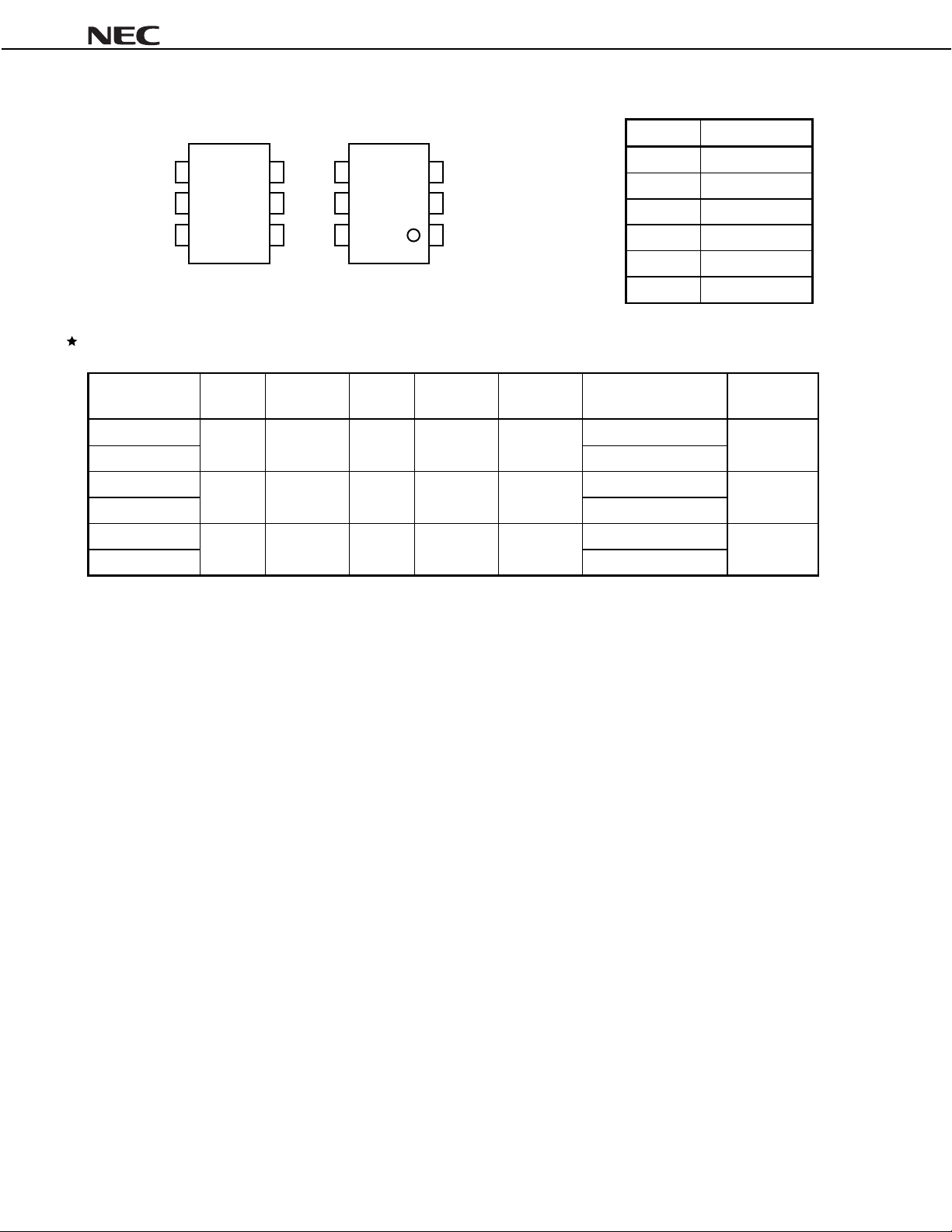
ORDERING INFORMATION
Part Number Package Marking Supplying Form
µ
PC2762TB-E3 C1Z
µ
PC2763TB-E3 6-pin super minimold C2A
µ
PC2771TB-E3 C2H
O(1 dB)
= +8.0 dBm TYP. @ 0.9 GHz
O(1 dB)
= +9.5 dBm TYP. @ 0.9 GHz
O(1 dB)
= +11.5 dBm TYP. @ 0.9 GHz
Embossed tape 8 mm wide.
1, 2, 3 pins face to perforat i on side of the tape.
Qty 3 kp/reel.
Remark
Document No. P12710EJ2V0DS00 (2nd edition)
Date Published June 1999 N CP(K)
Printed in Japan
To order evaluation samples, please contact your local NEC sales office.
(Part number for sample order:
The information in this document is subject to change without notice. Before using this document, please
confirm that this is the latest version.
Not all devices/types available in every country. Please check with local NEC representative for
availability and additional information.
PC2762TB, µPB2763TB, µPC2771TB)
µ
Caution Electro-static sensitive devices
The mark shows major revised points.
1997, 1999©
PIN CONNECTIONS
µµµµ
PC2762TB,
µµµµ
PC2763TB,
µµµµ
PC2771TB
(Top View)
3
2
1
Marking is an example of µPC2762TB
4
5
C1Z
6
PRODUCT LINE-UP (TA = +25 °C, VCC = V
u
Part No.
PC2762T 2.9 +8.0 +9.0 13 26.5 6-pin minimold
µ
PC2762TB 6-pin super minimold
µ
PC2763T 2.7 +9.5 +11.0 20 27.0 6-pin minimold
µ
PC2763TB 6-pin super minimold
µ
PC2771T 2.2 +11.5 +12.5 21 36.0 6-pin minimold
µ
PC2771TB 6-pin super minimold
µ
f
(GHz)
O (1 dB)
P
(dBm)
(Bottom View)
4
5
6
out
= 3.0 V, ZL = ZS = 50
O (sat)
P
(dBm)
3
2
1
)
ΩΩΩΩ
G
(dB)
P
CC
I
(mA)
Pin No. Pin Name
1 INPUT
2GND
3GND
4OUTPUT
5GND
6V
Package Marking
CC
C1Z
C2A
C2H
Remark
Notice
Typical performance. Please refer to ELECTRICAL CHARACTERISTICS in detail.
The package size distinguishes between minimold and super minimold.
2
Data Sheet P12710EJ2V0DS00

SYSTEM APPLICATION EXAMPLE
Digital cellular telephone
µµµµ
PC2762TB,
µµµµ
PC2763TB,
µµµµ
PC2771TB
RX
PLL
SW
TX
PA
The insertion point is different due to the specifications of conjunct devices.
Note
For conjunction with your devices, refer to the data sheets to confirm their conbination.
µ
PC2762TB
or
PC2763TB
µ
PC2771TB
µ
÷N
0 °
Phase
shifter
90 °
DEMO
PLL
I
Q
I
Q
Data Sheet P12710EJ2V0DS00
3

PIN EXPLANATION
µµµµ
PC2762TB,
µµµµ
PC2763TB,
µµµµ
PC2771TB
Pin
Pin Name
No.
1 INPUT – 1.31
4 OUTPUT Voltage
6VCC2.7 to 3.3 – Power supply pin, which biases
2
3
5
GND 0 – Ground pin. This pi n should be
Applied
Voltage
(V)
as same
CC
as V
through
external
inductor
Pin
Voltage
Note
(V)
1.01
0.97
– Signal output pi n. The inductor
Function and Applications Internal Equivalent Circ ui t
Signal input pin. A internal
matching circuit, configured with
resistors, enables 50
connection over a wide band.
A multi-feedback ci rcuit is
designed to cancel the
deviations of h
This pin must be coupled to
signal source with capac i t or for
DC cut.
must be attached between V
and output pins to supply
current to the internal output
transistors.
the internal input transis tor.
This pin should be externally
equipped with bypass capaci t or
to minimize its i m pedance.
connected to system ground
with minimum inductanc e.
Ground pattern on the board
should be formed as wide as
possible.
All the ground pins must be
connected together with wide
ground pattern to decrease
impedance difference.
Ω
FE
and resistance.
6
4
CC
1
*
3
GND GND
µ
* PC2762TB does not have
this capacitance.
5
2
Pin voltage is measured at V
Note
4
CC
= 3.0 V. Above: µPC2762TB, Center: µPC2763TB, Below: µPC2771TB.
Data Sheet P12710EJ2V0DS00

ABSOLUTE MAXIMUM RATINGS
Parameter Symbol Conditions
µµµµ
PC2762TB,
µµµµ
PC2763TB,
PC2762TB
µ
PC2763TB
µ
Ratings
µµµµ
PC2771TB
PC2771TB
µ
Unit
Supply Voltage V
Total Circuit Current I
Power Dissipation P
Operating Ambient
Temperature
Storage Temperature T
Input Power P
CC
CC
T
stg
TA = +25 °C, pin 4 and 6 3.6 V
TA = +25 °C 70 77.7 mA
D
Mounted on double copper clad
50 × 50 × 1.6 mm epoxy glass P WB
A
= +85 °C
T
A
in
TA = +25 °C+10+13dBm
RECOMMENDED OPERATING CONDITIONS
Parameter Symbol MIN. TYP. MAX. Unit Remark
Supply Voltage V
Operating Ambient
Temperature
Operating Frequency f
CC
A
T
opt
2.7 3.0 3.3 V Same voltage should be applied to pin
4 and 6.
40 +25 +85 °C
−
0.8
−
1.9 GHz Only for µPC2771TB
200 mW
40 to +85
−
55 to +150
−
−
C
°
C
°
Data Sheet P12710EJ2V0DS00
5

µµµµ
PC2762TB,
µµµµ
PC2763TB,
µµµµ
PC2771TB
ELECTRICAL CHARACTERISTICS (TA = +25 °C, VCC = V
PC2762TB,
µµµµ
Parameter S ymbol Test Conditions
Circuit Current I
Power Gain G
Noise Figure NF f = 0.9 GHz
Upper Limit Operating
Frequency
Isolation ISL f = 0.9 GHz
Input Return Loss RL
Output Return Loss RL
1 dB Gain Compression Output Level
PC2763TB
µµµµ
O (1 dB)
P
CC
f
P
u
in
out
No signal
f = 0.9 GHz
f = 1.9 GHz
f = 1.9 GHz
3 dB down below
from gain at
f = 0.1 GHz
f = 1.9 GHz
f = 0.9 GHz
f = 1.9 GHz
f = 0.9 GHz
f = 1.9 GHz
f = 0.9 GHz
f = 1.9 GHz
out
= 3.0 V, ZL = ZS = 50
PC2762TB
µ
MIN. TYP. MAX. MIN. TYP. MAX.
26.5 35.0
−
11
11.51315.51617.5
−
−
2.7 2.9
22
20
6.0
5.5
8.0
9.0
+5.5
+4.5
11.0
12.0
+8.0
+7.0
6.5
7.0
27
25
9.0
8.5
8.0
9.0
−
−
−
−
−
−
−
−
−
)
ΩΩΩΩ
PC2763TB
µ
27.0 35.0 mA
−
18
18
−
−
2.3 2.7
25
24
8.0
8.0
5.0
6.0
+7.0
+4.0
11.0
11.0
+9.5
+6.5
20
21
5.5
5.5
30
29
7.0
9.0
23
24
7.0
7.5
−
−
−
−
−
−
−
−
−
Unit
dB
dB
GHz
dB
dB
dB
dBm
PC2771TB
µµµµ
Parameter S ymbol Test Conditions
O (1 dB)
P
O (sat)
P
CC
f
No signal
P
f = 0.9 GHz
f = 1.5 GHz
f = 1.5 GHz
u
3 dB down below from gain at f = 0.1 GHz 1.8 2.2
f = 1.5 GHz
in
f = 0.9 GHz
f = 1.5 GHz
out
f = 0.9 GHz
f = 1.5 GHz
f = 0.9 GHz
f = 1.5 GHz
f = 0.9 GHz
f = 1.5 GHz
Circuit Current I
Power Gain G
Noise Figure NF f = 0.9 GHz
Upper Limit Operating
Frequency
Isolation ISL f = 0.9 GHz
Input Return Loss RL
Output Return Loss RL
1 dB Gain CompresSion Output Level
Saturated Output
Power Level
PC2771TB
µ
MIN. TYP. MAX.
36.0 45.0 mA
−
19
18
−
−
25
25
10
10
6.5
5.5
+9.0
+7.0
−
−
21
21
6.0
6.0
30
30
14
14
9.0
8.5
+11.5
+9.5
+12.5
+11
24
24
7.5
7.5
−
−
−
−
−
−
−
−
−
−
−
Unit
dB
dB
GHz
dB
dB
dB
dBm
dBm
6
Data Sheet P12710EJ2V0DS00

µµµµ
PC2762TB,
µµµµ
PC2763TB,
µµµµ
PC2771TB
STANDARD CHARACTERISTICS FOR REFERENCE (TA = +25 °C, VCC = V
PC2762TB,
µµµµ
Saturated
Output Power
Level
Adjacent channel
power
Third order
intermodulation
distortion PO
PC2771TB
µµµµ
PC2763TB
µµµµ
P
O (sat)
adj
P
3
IM
f = 0.9 GHz
f = 1.9 GHz
f = 0.9 GHz
/4 QPSK wave
π
PO = +4 dBm
2 sine wave input.
Output of each tone
(each)
= +4 dBm
Note
f = ±50 kHz
∆
f = ±100 kHz
∆
f1 = 0.900 GHz
2
= 0.902 GHz
f
1
f
= 1.900 GHz
2
= 1.902 GHz
f
PC2762TB
µ
MIN. TYP. MAX. MIN. TYP. MAX.
+9.0
−
+8.5
−
64
−
−
64
−
−
−−16−−−27−
−−10−−−14−
out
= 3.0 V, ZL = ZS = 50
Reference
PC2763TBParameter Symbol Test Conditions
µ
−
−
−
−
+11.0
−
−
−
−
+8.0
61
−
62
−
)
ΩΩΩΩ
Unit
dBm
−
−
dBc
−
−
dBc
dBc
Adjacent channel
power 1
Adjacent channel
power 2
Third order
intermodulation
distortion P
π/4 DQPSK modulated wave input, data rate 42 kbps, Filter roll off
Note
adj
P
1 f = 0.9 GHz
/4 QPSK wave
π
PO = +7 dBm
adj
P
2 f = 1.5 GHz
/4 QPSK wave
π
PO = +7 dBm
3
IM
2 sine wave input.
Output of each tone
O
(each)
Note
Note
= +7 dBm
f = ±50 kHz
∆
f = ±100 kHz
∆
f = ±50 kHz
∆
f = ±100 kHz
∆
f1 = 0.900 GHz
2
= 0.902 GHz
f
1
f
= 1.500 GHz
2
= 1.502 GHz
f
α
= 0.5, PN 9
Reference
PC2771TBParameter Symbol Test Conditions
µ
MIN. TYP. MAX.
−
−
−
−
−−18−
−−12−
61
−
−
−
−
72
59
71
−
−
−
−
Unit
dBc
dBc
dBc
dBc
Data Sheet P12710EJ2V0DS00
7
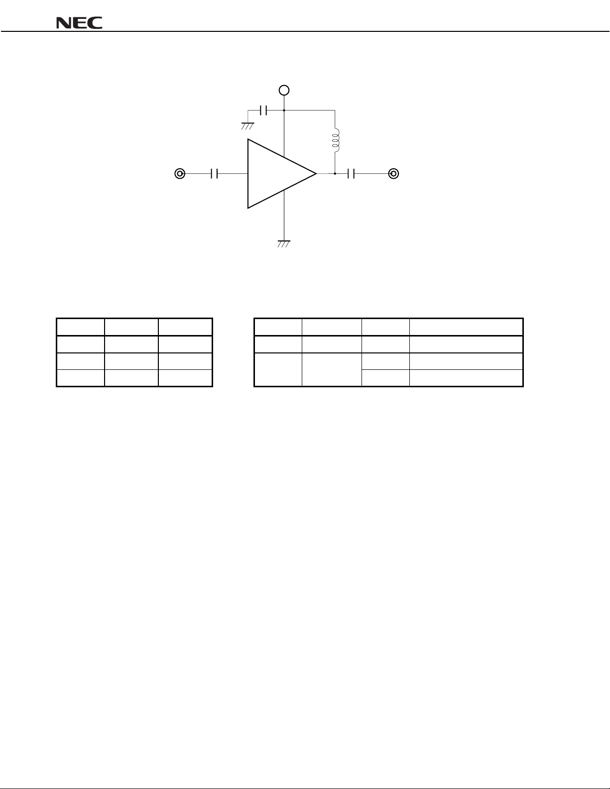
TEST CIRCUIT
1 000 pF
3
C
µµµµ
PC2762TB,
V
CC
µµµµ
PC2763TB,
µµµµ
PC2771TB
1
C
1 000 pF
6
1
2, 3, 5
4
L
C
2
1 000 pF
50 Ω50 Ω
OUTIN
COMPONENTS OF TEST CIRCUIT EXAMPLE OF ACTUAL APPLICATION COMPONENTS
FOR MEASURING ELECTRICAL
CHARACTERISTICS
Type Value Type Value Operating Frequency
2
C1, C
3
C
L Bias Tee 1 000 nH 10 nH 2.0 GHz or hi gher
Bias Tee 1 000 pF C1 to C3Chip capacitor 1 000 pF 100 MHz or higher
Capacitor 1 000 pF L Chip induc t or 100 nH 100 MHz or higher
INDUCTOR FOR THE OUTPUT PIN
The internal output transistor of this IC consumes 20 mA, to output medium power. To supply current for output
transistor, connect an inductor between the Vcc pin (pin 6) and output pin (pin 4). Select large value inductance, as
listed above.
The inductor has both DC and AC effects. In terms of DC, the inductor biases the output transistor with minimum
voltage drop to output enable high level. In terms of AC, the inductor make output-port-impedance higher to get
enough gain. In this case, large inductance and Q is suitable.
For above reason, select an inductance of 100 Ω or over impedance in the operating frequency. The gain is a
peak in the operating frequency band, and suppressed at lower frequencies.
The recommendable inductance can be chosen from example of actual application components list as shown
above.
CAPACITORS FOR THE VCC, INPUT, AND OUTPUT PINS
Capacitors of 1 000 pF are recommendable as the bypass capacitor for the Vcc pin and the coupling capacitors
for the input and output pins.
The bypass capacitor connected to the Vcc pin is used to minimize ground impedance of Vcc pin. So, stable bias
can be supplied against Vcc fluctuation.
The coupling capacitors, connected to the input and output pins, are used to cut the DC and minimize RF serial
impedance. Their capacitance are therefore selected as lower impedance against a 50 Ω load. The capacitors thus
perform as high pass filters, suppressing low frequencies to DC.
To obtain a flat gain from 100 MHz upwards, 1 000 pF capacitors are used in the test circuit. In the case of under
10 MHz operation, increase the value of coupling capacitor such as 10 000 pF. Because the coupling capacitors are
determined by equation, C = 1/(2πRfc).
8
Data Sheet P12710EJ2V0DS00

µµµµ
PC2762TB,
ILLUSTRATION OF THE TEST CIRCUIT ASSEMBLED ON EVALUATION BOARD
Top View
321
→
C1Z
456
Mounting direction
(Marking is an example for PC2762TB)
IN OUT
CC
µµµµ
PC2763TB,
AMP-2
L
CC
V
C
µµµµ
PC2771TB
COMPONENT LIST
Value
C 1 000 pF
L Example: 10 nH
For more information on the use of this IC, refer to the following application note: USAGE AND APPLICATION OF
SILICON MEDIUM-POWER HIGH-FREQUENCY AMPLIFIER MMIC (P12152E).
Notes
1.
30 × 30 × 0.4 mm double sided copper clad polyimide board.
2.
Back side: GND pattern
3.
Solder plated on pattern
4.
: Through holes
Data Sheet P12710EJ2V0DS00
9
 Loading...