How it Works
Log In / Sign Up
0
My Files
0
My Downloads
329097
History
Account Settings
Log Out
Buy Points
How it Works
FAQ
Contact Us
Questions and Suggestions
Users
NEC
Loading...
U
UPC2708TB-E3
UPC2709TB-E3
UPC2712TB-E3
UPC2746T
UPC2749TB-E3
UPC2758TB-E3
UPC2766GS-E1
UPC2771TB-E3
UPC2775GS-E1
UPC2903HF
UPC29M09HB
UPC78M15AHF
UPC7908AHF
UPC79N24H
UPC8109TB
UPC8110GR-E1
UPC8120T-E3
UPC8131TA-E3
UPC8152TA
UPC8158K-E1
UPD16676W
UPD16681W-011
UPD16855AG
UPD16873MC-6A4
uPD1703C-015
UPD17P204GC-002-3BH
UPD17P207GF-003-3B9
UPD30500S2-200
uPD43256G-12
UPD45128841G5-A10-9JF
UPD4704G
UPD4713AGT
UPD488448FF-C80-45-DQ1
UPD4992GS-T2
UPD6379LGR
uPD65655
UPD6P4BMC-5A4
uPD70008C
uPD70108G-8
uPD70108GC-5-3B6
uPD70116HLM-16
UPD70216HLP-20
UPD70433R-12
UPD70F3017AYF1-EA6
uPD71054G
UPD71055L-8
UPD72107GC-3B9
UPD7225GB-3B7
UPD750004CU-A-XXX
UPD75008GB-A-XXX-3B4
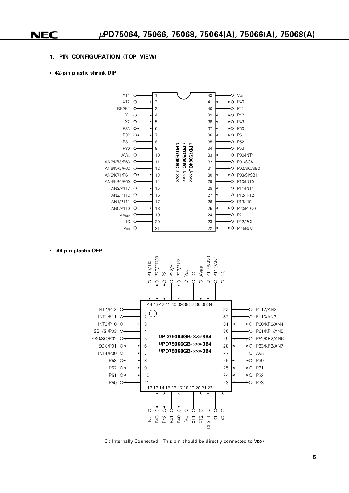
UPD75068GB-XXX-3B4
UPD75108AGC-XXX-AB8
UPD75108GF-XXX-3BE
UPD75116FGF-XXX-3BE
UPD75116GF-XXX-3BE
UPD75117HGK-XXX-8A8
UPD75208G-XXX-1B
UPD75216ACW-XXX
UPD75237GJ-XXX-5BG
UPD753108GK-XXX-8A8
UPD75316BGC-XXX-3B9
UPD75316GF-XXX-3B9
UPD753208GT-XXX-T2
UPD75402AGB-A-XXX-3B4
uPD75CG08E
UPD75P036KG
UPD75P3018GK-BE9
uPD780318
UPD784031YGK-BE9
UPD789104CT-XXX
UPD78CP14GF-3BE
uPD78F4218AYGF-3BA
UPD78P322GF-3B9
UPG103P
UPG2110TB-E3
V
V191W
V221W-BK
V230X
2
V260
2
V28 0799-20
V300X
V302W
V302X
V311X
V332X
V404-T
V422
V461
V462
V651-PC
V652
V850ES-FF3
V850ES-Fx3
V850ES-SJ3
V850-SV1
VC-7700
VE303X
VE303XG
Versa
versa 2000
Loading...
Loading...
Nothing found
UPD75068GB-XXX-3B4
Datasheet
68 pgs
643.12 Kb
0
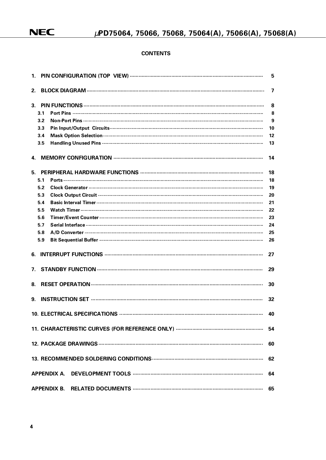
Table of contents
Loading...
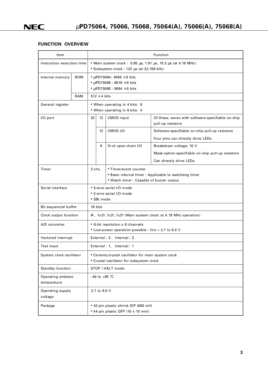
NEC UPD75068GB-XXX-3B4, UPD75068GB-A-XXX-3B4, UPD75068CU-A-XXX, UPD75068CU-XXX, UPD75066GB-XXX-3B4 Datasheet
...
NEC UPD75068GB-XXX-3B4, UPD75068GB-A-XXX-3B4, UPD75068CU-A-XXX, UPD75068CU-XXX, UPD75066GB-XXX-3B4, UPD75066GB-A-XXX-3B4, UPD75066CU-A-XXX, UPD75066CU-XXX, UPD75064GB-XXX-3B4, UPD75064GB-A-XXX-3B4, UPD75064CU-A-XXX, UPD75064CU-XXX Datasheet
Download
Loading...
+
47
hidden pages
Unhide
You need points to download manuals.
1 point = 1 manual.
You can buy points or you can get point for every manual you upload.
Buy points
Upload your manuals


 Loading... Loading...