


NEC UPD75108GF-XXX-3BE, UPD75108GF-A-XXX-3BE, UPD75108G-XXX-1B, UPD75108CW-XXX, UPD75108CW-A-XXX Datasheet
...
DESCRIPTION
µ
PD75108 is a 4-bit single-chip microcomputer integrating timer/event counters, serial interface, and vector
interrupt function, in addition to a CPU, ROM, RAM, and I/O ports, on a single chip. Operating at high speeds,
the microcomputer allows data to be manipulated in units of 1, 4, or 8 bits. In addition, various bit manipulation
instructions are provided to reinforce I/O manipulation capability. Equipped with I/Os for interfacing with
peripheral circuits operating on a different supply voltage, outputs that can directly drive LEDs, and analog
inputs,
µ
PD75108 is suitable for controlling such systems as VTRs, acoustic products, button telephones, radio
communications equipment, and printers. A pin-compatible EPROM model is also available for evaluation of
system development and small-scale production of application systems.
Detailed functions are described in the following user’s manual. Be sure to read it for designing.
µ
PD751XX Series User’s Manual: IEM-922
FEATURES
• Internal memory
• Program memory (ROM)
: 8068 × 8 bits (µPD75108)
: 6016
×
8 bits (µPD75106)
: 4096
×
8 bits (µPD75104)
• Data memory (RAM)
: 512 × 4 bits (µPD75108)
: 320
×
4 bits (µPD75106, 75104)
• New architecture “75X series” rivaling 8-bit microcomputers
• 43 systematically organized instructions
• A wealth of bit manipulation instructions
• 8-bit data transfer, compare, operation, increment, and decrement instructions
• 1-byte relative branch instructions
• GETI instruction executing 2-/3-byte instruction with one byte
• High speed. Minimum instruction execution time: 0.95
µ
s (at 4.19 MHz), 5 V
• Power-saving, instruction time change function: 0.95
µ
s/1.91 µs/15.3 µs (at 4.19 MHz)
• I/O port pins as many as 58
• Three channels of 8-bit timers
• 8-bit serial interface
• Multiplexed vector interrupt function
• Model with PROM is available:
µ
PD75P108B (One-time PROM, EPROM)
NEC Corporation 1989
Document No. IC-2520B
(O. D. No. IC-6906B)
Date Published January 1994 P
Printed in Japan
DATA SHEET
MOS INTEGRATED CIRCUIT
µ
PD75104, 75106, 75108
4-BIT SINGLE-CHIP MICROCOMPUTER
The mark ★ shows major revised points.
The information in this document is subject to change without notice.
Unless there are differences among µPD75104, 75106, and 75108 functions, µPD75108 is treated as the
representative model throughout this manual.

µ
PD75104, 75106, 75108
2
ORDERING INFORMATION
Part Number Package Quality Grade
µ
PD75104CW-xxx 64-pin plastic shrink DIP (750 mil) Standard
µ
PD75104GF-xxx-3BE 64-pin plastic QFP (14 × 20 mm) Standard
µ
PD75106CW-xxx 64-pin plastic shrink DIP (750 mil) Standard
µ
PD75106GF-xxx-3BE 64-pin plastic QFP (14 × 20 mm) Standard
µ
PD75108CW-xxx 64-pin plastic shrink DIP (750 mil) Standard
µ
PD75108GF-xxx-3BE 64-pin plastic QFP (14 × 20 mm) Standard
Remarks: xxx is ROM code number.
Please refer to “Quality Grade on NEC Semiconductor Devices” (Document Number IEI-1209) published by
NEC Corporation to know the specification of quality grade on the devices and its recommended applications.

µ
PD75104, 75106, 75108
3
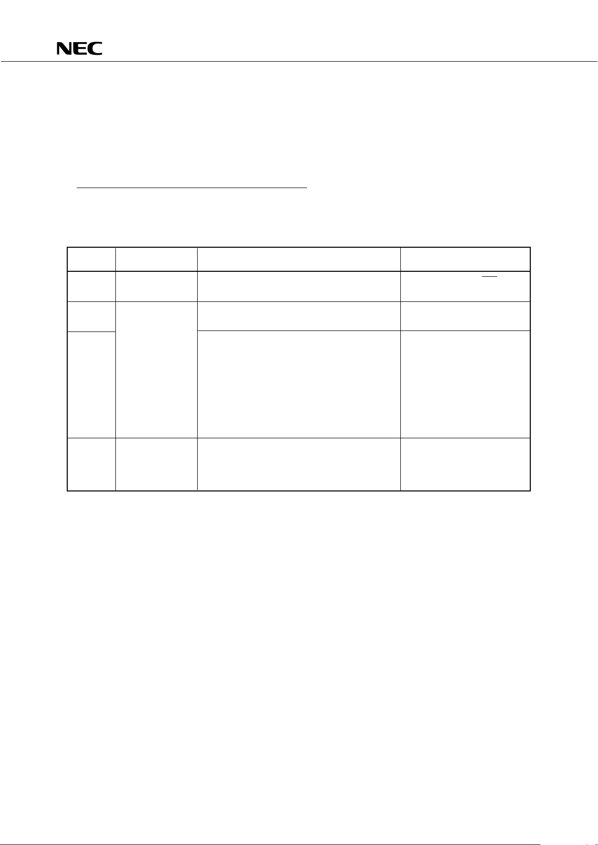
FUNCTIONAL OUTLINE
Item Specifications
Number of Basic Instructions 43
Minimum Instruction Changeable in three steps: 0.95 µs, 1.91 µs, and 15.3 µs at 4.19 MHz
Execution Time
ROM 8064 × 8 bits (µPD75108), 6016 × 8 bits (µPD75106), 4096 × 8 bits (µPD75104)
RAM 512 × 4 bits (µPD75108), 320 × 4 bits (µPD75106, 75104)
General-Purpose Register 4 bits × 8 × 4 banks (memory mapped)
Three accumulators selectable according to the bit length of manipulated data:
• 1-bit accumulator (CY), 4-bit accumulator (A), and 8-bit accumulator (XA)
58 port pins
• CMOS input pins: 10
I/O Port
• CMOS I/O pins (can directly drive LEDs): 32
• Medium voltage N-ch open-drain I/O pins: 12
(can directly drive LEDs. Pull-up resistor can be connected to each bit)
• Comparator input pins (4-bit accuracy): 4
• 8-bit timer/event counter × 2
Timer/Counter
• 8-bit basic interval timer (can be used as watchdog timer)
• 8 bits
Serial Interface • LSB first/MSB first mode selectable
• Two transfer modes (transfer/reception and reception only modes)
Vector Interrupt External: 3, Internal: 4
Test Input External: 2
Standby • STOP and HALT modes
• Various bit manipulation instructions (set, reset, test, Boolean operation)
Instruction Set
• 8-bit data transfer, compare, operation, increment, and decrement
• 1-byte relative branch instructions
• GETI instruction constituting 2 or 3-byte instruction with 1 byte
• Power-ON reset circuit (mask option)
Others
• Bit manipulation memory (bit sequential buffer: 16 bits)
Package
• 64-pin plastic shrink DIP (750 mil)
• 64-pin plastic QFP (14 × 20 mm)
Internal Memory
Accumulator

µ
PD75104, 75106, 75108
4
CONTENTS
1. PIN CONFIGURATION (TOP VIEW)............................................................................................... 6
2. BLOCK DIAGRAM ........................................................................................................................... 8
3. PIN FUNCTIONS.............................................................................................................................. 9
3.1 PORT PINS............................................................................................................................................. 9
3.2 PINS OTHER THAN PORTS ................................................................................................................. 10
3.3 PIN INPUT/OUTPUT CIRCUITS ........................................................................................................... 11
3.4 RECOMMENDED PROCESSING OF UNUSED PINS .......................................................................... 12
3.5 NOTES ON USING THE P00/INT4, AND RESET PINS ...................................................................... 13
4. MEMORY CONFIGURATION .......................................................................................................... 14
5. PERIPHERAL HARDWARE FUNCTIONS........................................................................................ 20
5.1 PORTS .................................................................................................................................................... 20
5.2 CLOCK GENERATOR CIRCUIT ............................................................................................................ 21
5.3 CLOCK OUTPUT CIRCUIT .................................................................................................................... 22
5.4 BASIC INTERVAL TIMER ..................................................................................................................... 23
5.5 TIMER/EVENT COUNTER ..................................................................................................................... 23
5.6 SERIAL INTERFACE .............................................................................................................................. 25
5.7 PROGRAMMABLE THRESHOLD PORT (ANALOG INPUT PORT) .................................................... 27
5.8 BIT SEQUENTIAL BUFFER .... 16 BITS ............................................................................................... 28
5.9 POWER-ON FLAG (MASK OPTION) .................................................................................................... 28
6. INTERRUPT FUNCTIONS................................................................................................................ 28
7. STANDBY FUNCTIONS .................................................................................................................. 30
8. RESET FUNCTION........................................................................................................................... 31
9. INSTRUCTION SET ......................................................................................................................... 34

µ
PD75104, 75106, 75108
5
10. APPLICATION EXAMPLES .............................................................................................................. 43
10.1 VTR SYSTEM CONTROLLER ............................................................................................................... 43
10.2 VTR CAMERA ........................................................................................................................................ 43
10.3 COMPACT DISC PLAYER ..................................................................................................................... 44
10.4 AUTOMOBILE APPLICATIONS (TRIP COMPUTER)............................................................................ 44
10.5 PUSHBUTTON TELEPHONE ................................................................................................................ 45
10.6 DISPLAY PAGER ................................................................................................................................... 45
10.7 PLAIN PAPER COPIER (PPC) ............................................................................................................... 46
10.8 PRINTER CONTROLLER ....................................................................................................................... 46
11. MASK OPTION SELECTION ........................................................................................................... 47
12. ELECTRICAL SPECIFICATIONS ...................................................................................................... 48
13. CHARACTERISTIC DATA ................................................................................................................ 57
14. PACKAGE DRAWINGS ................................................................................................................... 62
15. RECOMMENDED SOLDERING CONDITIONS ............................................................................... 65
APPENDIX A. FUNCTIONAL DIFFERENCES AMONG PRODUCTS IN µPD751XX SERIES ......... 66
APPENDIX B. DEVELOPMENT TOOLS .............................................................................................. 67
APPENDIX C. RELATED DOCUMENTS .............................................................................................. 68
µ
PD75104, 75106, 75108
6
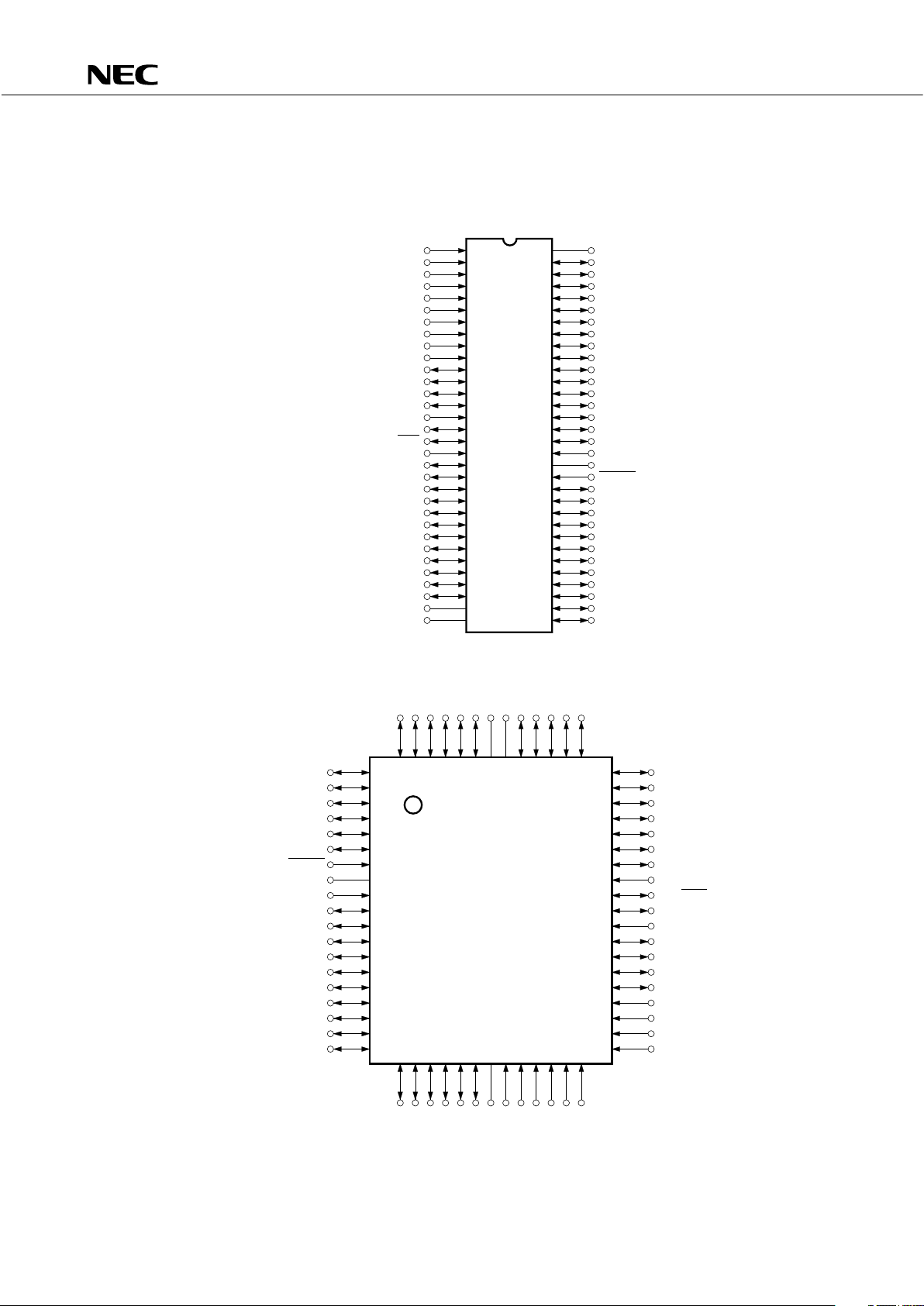
1. PIN CONFIGURATION (Top View)
• 64-Pin Plastic Shrink DIP (750 mil)
P13/INT3 1
V32
V64
33
SS
µ
PD75104CW-
PD75106CW-
PD75108CW-
×××
×××
×××
P12/INT2
P11/INT1
P10/INT0
PTH03
PTH02
PTH01
PTH00
TI0
TI1
P23
P22/PCL
2
3
4
5
6
7
8
9
10
11
12
P21 PTO1 13
P20 PTO0 14
P9063
P9162
P9261
P9360
P8059
P8158
P8257
P8356
P7055
P7154
P7253
P7352
P6051
P03/SI 15 P6150
P02/SO 16 P6249
P01/SCK 17 P6348
P00/INT4 18 X147
P123 19 X246
P122 20 RESET45
P121 21 P5044
P120 22 P5143
P133 23 P5242
P132 24 P5341
P131 25 P4040
P130 26 P4139
P143 27 P4238
P142 28 P4337
P141 29 P3036
P140 30 P3135
NC 31 P3234
DD
µ
µ
P33
51 P1311P41
64
P42
P43
P30
P31
P32
P33VNC
P140
P141
P142
P143
P130
63 62 61 60 59 58 57 56 55 54 53 52
DD
20 21 22 23 24 25 26 27 28 29 30 31 32
P81
P80
P93
P92
P91
P90
V
P13/INT3
P12/INT2
P11/INT1
P10/INT0
PTH03
PTH02
SS
µ
PD75104GF-
PD75106GF-
PD75108GF-
×××
×××
×××
µ
µ
-3BE
-3BE
-3BE
50 P1322P40
49 P1333P53
48 P1204P52
47 P1215P51
46 P1226P50
45 P1237RESET
44 P00/INT48X2
43 P01/SCK9X1
42 P02/SO10P63
41 P03/SI11P62
40 P20/PTO012P61
39 P21/PTO113P60
38 P22/PCL14P73
37 P2315P72
36 TI116P71
35 TI017P70
34 PTH0018P83
33 PTH0119P82
• 64-Pin Plastic QFP (14 × 20 mm)

µ
PD75104, 75106, 75108
7
Pin names
P00-P03 : Port 0 SCK : Serial Clock Input/Output
P10-P13 : Port 1 SO : Serial Output
P20-P23 : Port 2 SI : Serial Input
P30-P33 : Port 3 PTO0, PTO1 : Timer Output
P40-P43 : Port 4 PCL : Clock Output
P50-P53 : Port 5 PTH00-PTH03 : Comparator Input
P60-P63 : Port 6
INT0, INT1, INT4 : External Vector Interrupt Input
P70-P73 : Port 7 INT2, INT3 : External Test Input
P80-P83 : Port 8 TI0, TI1 : Timer Input
P90-P93 : Port 9 X1, X2 : Clock Oscillation Pin
P120-P123 : Port 12 RESET : Reset Input
P130-P133 : Port 13 NC : No Connection
P140-P143 : Port 14
µ
PD75104, 75106, 75108
8
2. BLOCK DIAGRAM
TI0
PTO0/P20
BASIC
INTERVAL
TIMER
INTBT
PROGRAM
COUNTER*
ALU
CY SP (8)
BANK
GENERAL REG.
DECODE
AND
CONTROL
ROM
PROGRAM
MEMORY
8064 8BITS
: PD75108
6016 8BITS
: PD75106
4096 8BITS
: PD75104
µ
µ
µ
RAM
DATA MEMORY
512 4BITS
: PD75108
320 4BITS
: PD75106, 75104
×
×
×
×
×
µ
µ
f /2
XX
N
CPU CLOCK
Φ
PCL/P22 X1 X2 V
DDVSS
RESET
CLOCK
OUTPUT
CONTROL
CLOCK
DIVIDER
CLOCK
GENERATOR
STAND BY
CONTROL
TIMER/EVENT
COUNTER
#0
TIMER/EVENT
COUNTER
#1
SERIAL
INTERFACE
INTERRUPT
CONTROL
PROGRAMMABLE
THRESHOLD
PORT #0
TI1
PTO1/P21
SI/P03
SO/P02
SCK/P01
INT0/P10
INT1/P11
INT2/P12
INT3/P13
INT4/P00
PTH00-PTH03 4
4
4
4
4
4
4
4
4
4
4
4
4
4
BIT SEQ.
BUFFER (16)
PORT 0
P00 - P03
P10 - P13PORT 1
PORT 2
PORT 3
PORT 4
PORT 5
PORT 6
PORT 7
PORT 8
PORT 9
PORT 12
PORT 13
PORT 14
P20 - P23
P30 - P33
P40 - P43
P50 - P53
P60 - P63
P70 - P73
P80 - P83
P90 - P93
P120 - P123
P130 - P133
P140 - P143
*: 13 bits: PD75106, 75108
12 bits: PD75104
µ
µ
INTT0
INTT1
INTSIO
µ
PD75104, 75106, 75108
9
3. PIN FUNCTIONS
3.1 PORT PINS
I/O
Pin Name I/O
Shared with:
Function At Reset Circuit
TYPE*
1
P00 Input INT4 B
P01 I/O SCK F
4-bit input port (PORT 0) Input
P02 I/O SO E
P03 Input SI B
x
P10 INT0
P11 INT1
Input 4-bit input port (PORT 1) Input B
P12 INT2
P13 INT3
P20*
3
PTO0
P21*
3
PTO1
I/O 4-bit I/O port (PORT 2) Input E
P22*
3
PCL
x
P23*
3
—
4-bit programmable I/O port (PORT 3)
P30-P33*
3
I/O — Input E
Can be specified for input or output bitwise.
P40-P43*
3
I/O — 4-bit I/O port (PORT 4) Input E
o
P50-P53*
3
I/O — 4-bit I/O port (PORT 5) Input E
4-bit programmable I/O port (PORT 6)
P60-P63*
3
I/O — Input E
Can be specified for input or output bitwise. o
P70-P73*
3
I/O 4-bit I/O port (PORT 7) Input E
P80-P83*
3
I/O — 4-bit I/O port (PORT 8) Input E
o
P90-P93*
3
I/O — 4-bit I/O port (PORT 9) Input E
4-bit N-ch open-drain I/O port (PORT 12)
Built-in pull-up resistors can be specified in bit
P120-P123*
3
I/O —
units by mask option.
Open-drain withstanding voltage: 12 V
o
4-bit N-ch open-drain I/O port (PORT 13)
Built-in pull-up resistors can be specified in bit
P130-P133*
3
I/O —
units by mask option.
Open-drain withstanding voltage: 12 V
4-bit N-ch open-drain I/O port (PORT 14)
Built-in pull-up resistors can be specified in bit
P140-P143*
3
I/O — – Input*
2
M
units by mask option.
Open-drain withstanding voltage: 12 V
*1: Circles indicate Schmitt trigger input pins.
2: With drain open: high impedance
With pull-up resistor connected: high level
3: Can directly drive LEDs.
8-Bit
I/O
Input*
2
M
Input*
2
M
µ
PD75104, 75106, 75108
10
3.2 PINS OTHER THAN PORTS
I/O
Pin Name I/O
Shared with:
Function At Reset Circuit
TYPE*
1
PTH00-PTH03 Input — 4-bit variable threshold voltage analog input port — N
TI0 External event pulse inputs for timer/event counter.
Input — Also serves as edge-detected vector interrupt input. — B
TI1
1-bit input also possible.
PTO0 P20
I/O Outputs for timer/event counter Input E
PTO1 P21
SCK I/O P01 Serial clock I/O Input F
SO I/O P02 Serial data output Input E
SI Input P03 Serial data input Input B
Edge-detected vectored interrupt input (both rising and
INT4 Input P00 Input B
falling edges detected)
INT0 P10 Edge-detected vectored interrupt inputs (valid
Input Input B
INT1 P11 edge selectable)
INT2 P12
Input Edge-detected testable inputs (rising edge detected) Input B
INT3 P13
PCL I/O P22 Clock output Input E
Crystal/ceramic system clock oscillator connections.
X1, X2 — — Input external clock to X1, and signal in reverse phase — —
with X1 to X2.
RESET Input — System reset input (low level active type) — B
NC*
2
— — No Connection — —
VDD — — Positive power supply — —
VSS ——GND ——
*1: Circles indicate Schmitt trigger input pins.
2: Connect the NC pin directly to the V
DD pin when
µ
PD75P108B and a printed circuit board are shared.
µ
PD75104, 75106, 75108
11
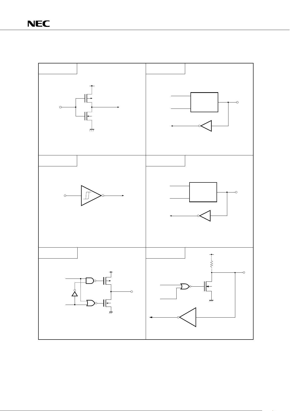
3.3 PIN INPUT/OUTPUT CIRCUITS
The following shows a simplified input/output circuit diagram for each pin of the
µ
PD75108.
TYPE A
TYPE E
TYPE B
TYPE F
IN
V
DD
Input buffer of CMOS standard
P–ch
N–ch
IN
Schmitt trigger input with hysteresis characteristics
data
output
disable
Type D
Type A
IN/OUT
TYPE D
TYPE M
data
output
disable
Type D
Type B
IN/OUT
data
output
disable
OUT
Push – pull output that can be set in a output
high– impedance state (both P –ch and N –ch are off)
V
DD
P-ch
N-ch
I/O circuit consisting of Type D push-pull output circuit
and Type A input buffer
I/O circuit consisting of Type D push-pull output and Type
B Schmitt trigger input
V
DD
P.U.R.
(mask option)
IN/OUT
data
output
disable
N-ch
(+12 V
withstand)
Medium-voltage input
buffer (+12 V withstand)
P.U.R.: Pull-Up Resistor
µ
PD75104, 75106, 75108
12
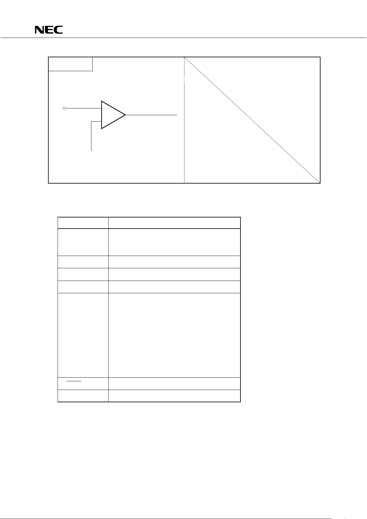
TYPE N
IN +
–
Comparator
V (threshold voltage)
REF
3.4 RECOMMENDED PROCESSING OF UNUSED PINS
Pin Recommended connections
PTH00-PTH03
TI0 Connect to VSS or VDD
TI1
P00 Connect to VSS
P01-P03 Connect to VSS or VDD
P10-P13 Connect to VSS
P20-P23
P30-P33
P40-P43
P50-P53
P60-P63 Input: Connect to VSS or VDD
P70-P73
P80-P83 Output: Open
P90-P93
P120-P123
P130-P133
P140-P143
RESET*
1
Connect to VDD
NC*
2
Open
*1: Connect this pin to the VDD pin only when a power-ON reset circuit
is provided as a mask option.
2: Connect the NC pin to the V
DD pin when
µ
PD75P108 and a printed
circuit board are shared.
µ
PD75104, 75106, 75108
13
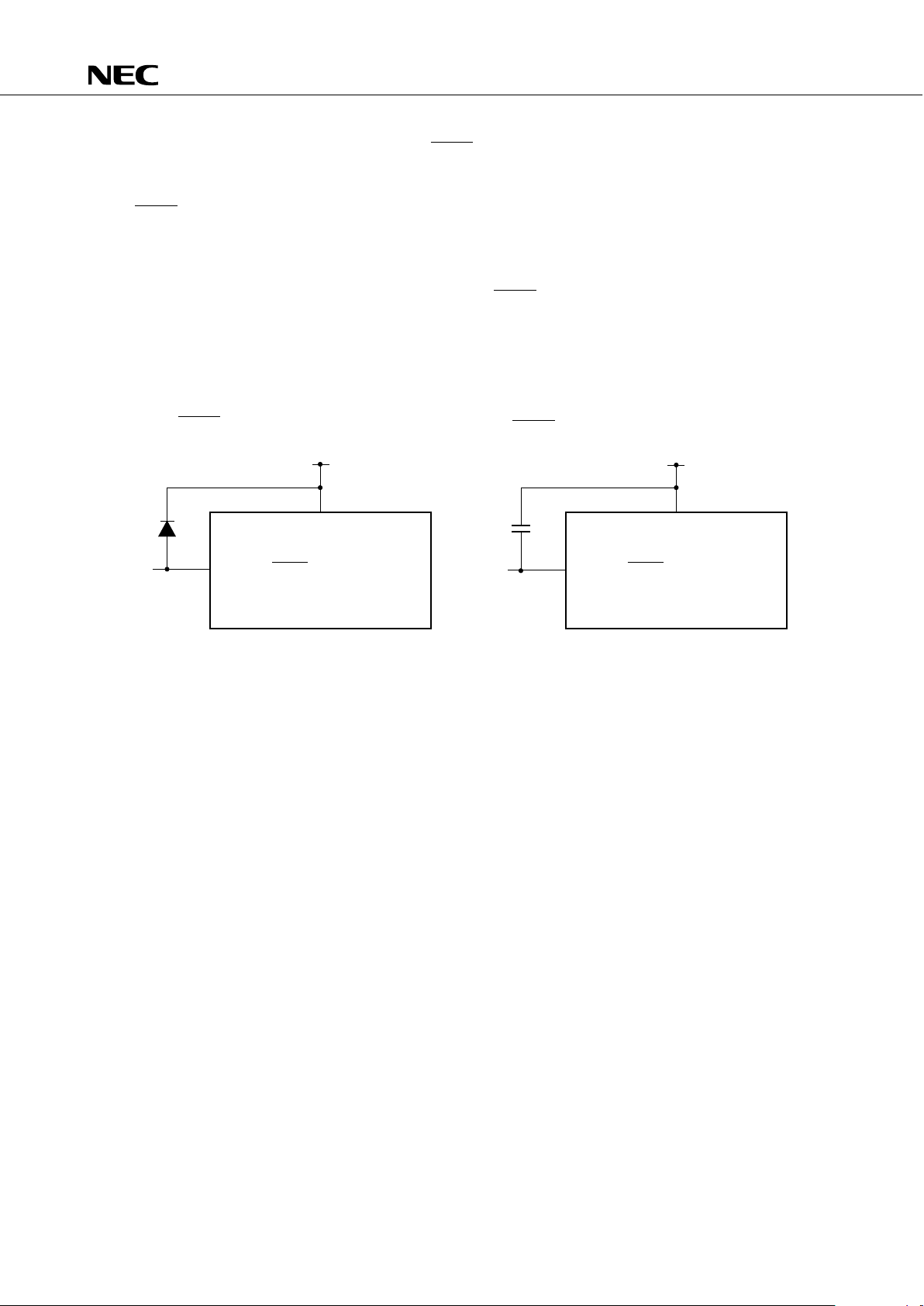
3.5 NOTES ON USING THE P00/INT4, AND RESET PINS
In addition to the functions described in Sections 3.1 and 3.2, an exclusive function for setting the test mode,
in which the internal fuctions of the
µ
PD75108 are tested (solely used for IC tests), is provided to the P00/INT4
and
RESET
pins.
If a voltage exceeding V
DD is applied to either of these pins, the
µ
PD75108 is put into test mode. Therefore,
even when the
µ
PD75108 is in normal operation, if noise exceeding the VDD is input into any of these pins, the
µ
PD75108 will enter the test mode, and this will cause problems for normal operation.
As an example, if the wiring to the P00/INT4 pin or the
RESET
pin is long, stray noise may be picked up
and the above montioned problem may occur.
Therefore, all wiring to these pins must be made short enough to not pick up stray noise. If noise cannot
be avoided, suppress the noise using a capacitor or diode as shown in the figure below.
• Connect a capacitor across P00/INT4 and
RESET
, and VDD.
• Connect a diode across P00/INT4 and
RESET
, and VDD.
VDD
VDD
P00/INT4, RESET
VDD
VDD
P00/INT4, RESET

µ
PD75104, 75106, 75108
14
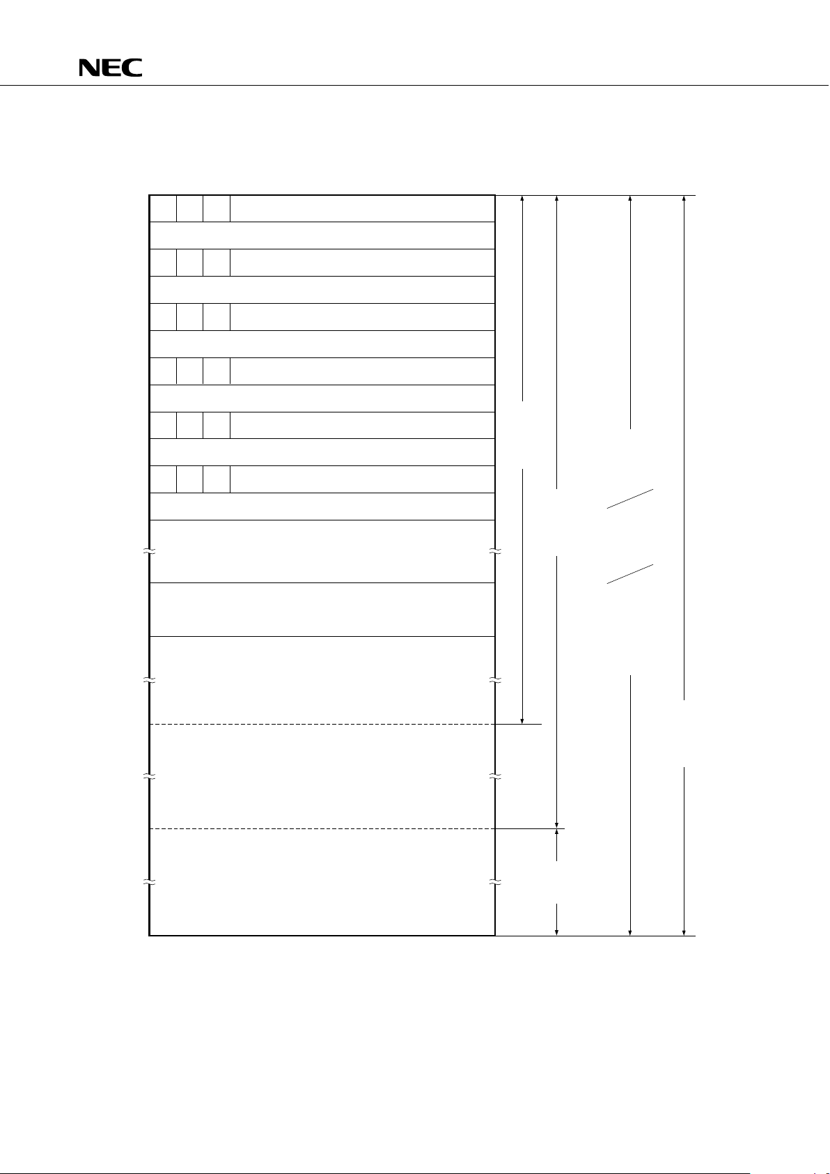
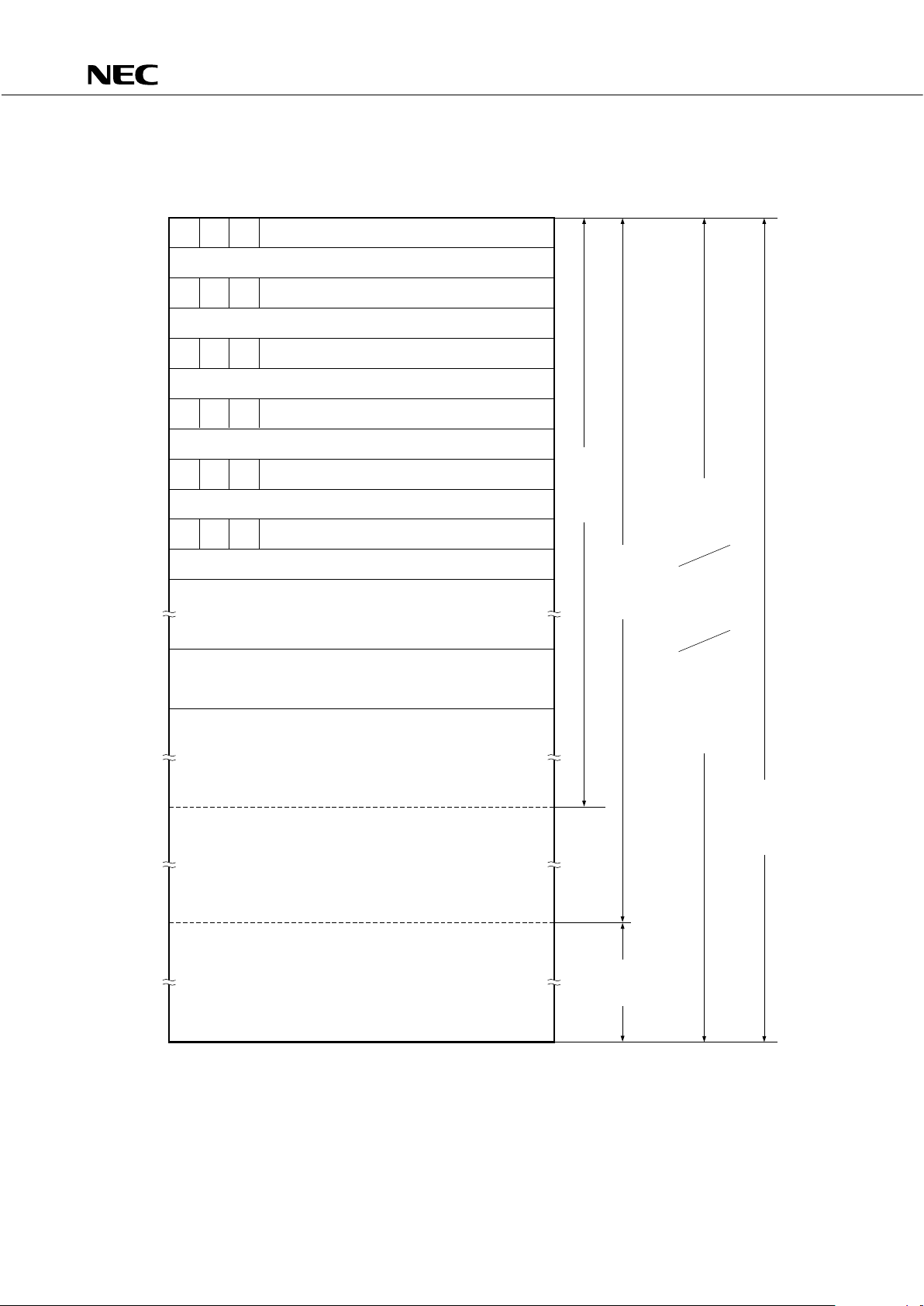
4. MEMORY CONFIGURATION
• Program memory (ROM) ... 8064 × 8 bits (0000H-1F7FH) : µPD75108
... 6016 × 8 bits (0000H-177FH) :
µ
PD75106
... 4096 × 8 bits (0000H-0FFFH) :
µ
PD75104
• 0000H, 0001H : Vector table to which address from which program is started is written after reset
• 0002H-000BH: Vector table to which address from which program is started is written after interrupt
• 0020H-007FH: Table area referenced by GETI instruction
• Data memory (RAM)
• Data area ....512 × 4 bits (000H–1FFH):
µ
PD75108
320 × 4 bits (000H-13FH) :
µ
PD75106, 75104
• Peripheral hardware area .... 128 × 4 bits (F80H–FFFH)
µ
PD75104, 75106, 75108
15
(a) µPD75108
765
MBE RBE 0
MBE RBE 0
MBE RBE 0
MBE RBE 0
MBE RBE 0
MBE RBE 0
Internal reset start address (upper 5 bits)
Internal reset start address (lower 8 bits)
INTBT/INT4 start address (upper 5 bits)
INTBT/INT4 start address (lower 8 bits)
INT0/INT1 start address (upper 5 bits)
INT0/INT1 start address (lower 8 bits)
INTSIO start address (upper 5 bits)
INTSIO start address (lower 8 bits)
INTT0 start address (upper 5 bits)
INTT0 start address (lower 8 bits)
INTT1 start address (upper 5 bits)
INTT1 start address (lower 8 bits)
0000H
0002H
0004H
0006H
0008H
000AH
0020H
007FH
0080H
07FFH
0800H
0FFFH
1000H
1F7FH
GETI instruction reference table
0
BRCB
! caddr
instruction
branch
address
CALLF
! faddr
instruction
entry
address
BR ! addr
instruction
branch address
CALL ! addr
instruction
subroutine
entry address
BR $addr
instruction
relational
branch address
(–15 to –1,
+2 to +16)
Branch destination
address and
subroutine entry
address for
GETI instruction
Address
BRCB ! caddr
instruction
branch address
Remarks: In addition to the above addresses, program can be branched to addresses specified by the PC
with the contents of its lower 8 bits changed by BR PCDE or BR PCXA instruction.
Fig. 4-1 Program Memory Map (1/3)
µ
PD75104, 75106, 75108
16
(b) µPD75106
Remarks: In addition to the above addresses, program can be branched to addresses specified by the PC
with the contents of its lower 8 bits changed by BR PCDE or BR PCXA instruction.
Fig. 4-1 Program Memory Map (2/3)
765
MBE RBE 0
MBE RBE 0
MBE RBE 0
MBE RBE 0
MBE RBE 0
MBE RBE 0
Internal reset start address (upper 5 bits)
Internal reset start address (lower 8 bits)
INTBT/INT4 start address (upper 5 bits)
INTBT/INT4 start address (lower 8 bits)
INT0/INT1 start address (upper 5 bits)
INT0/INT1 start address (lower 8 bits)
INTSIO start address (upper 5 bits)
INTSIO start address (lower 8 bits)
INTT0 start address (upper 5 bits)
INTT0 start address (lower 8 bits)
INTT1 start address (upper 5 bits)
INTT1 start address (lower 8 bits)
0000H
0002H
0004H
0006H
0008H
000AH
0020H
007FH
0080H
07FFH
0800H
0FFFH
1000H
177FH
GETI instruction reference table
0
BRCB
! caddr
instruction
branch
address
CALLF
! faddr
instruction
entry
address
BR ! addr
instruction
branch address
CALL ! addr
instruction
subroutine
entry address
BR $addr
instruction
relational
branch address
(–15 to +16)
Branch destination
address and
subroutine entry
address for
GETI instruction
Address
BRCB ! caddr
instruction
branch address
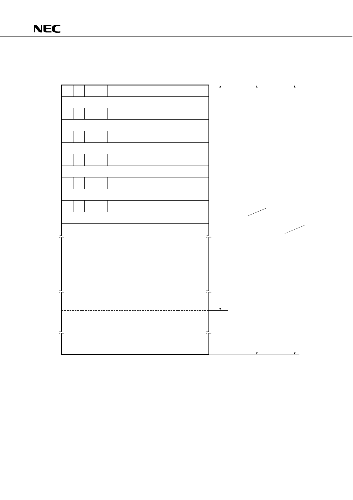
µ
PD75104, 75106, 75108
17
(c) µPD75106
765
MBE RBE 0
MBE RBE 0
MBE RBE 0
MBE RBE 0
MBE RBE 0
MBE RBE 0
Internal reset start address (upper 4 bits)
Internal reset start address (lower 8 bits)
INTBT/INT4 start address (upper 4 bits)
INTBT/INT4 start address (lower 8 bits)
INT0/INT1 start address (upper 4 bits)
INT0/INT1 start address (lower 8 bits)
INTSIO start address (upper 4 bits)
INTSIO start address (lower 8 bits)
INTT0 start address (upper 4 bits)
INTT0 start address (lower 8 bits)
INTT1 start address (upper 4 bits)
INTT1 start address (lower 8 bits)
000H
002H
004H
006H
008H
00AH
020H
07FH
080H
7FFH
800H
FFFH
GETI instruction reference table
0
CALLF
! faddr
instruction
entry
address
BRCB ! caddr
instruction
branch address
CALL ! addr
instruction
subroutine
entry address
Address
4
0
0
0
0
0
0
BR $addr
instruction
relational
branch address
(–15 to +16)
Branch destination
address and
subroutine entry
address for
GETI instruction
Remarks: In addition to the above addresses, program can be branched to addresses specified by the PC
with the contents of its lower 8 bits changed by BR PCDE or BR PCXA instruction.
Fig. 4-1 Program Memory Map (3/3)
µ
PD75104, 75106, 75108
18
(a) µPD75108
000H
01FH
0FFH
100H
1FFH
F80H
FFFH
Data memory
Memory bank
(32 × 4)
256× 4
Not provided
128× 4
Bank 0
General-purpose
register area
Stack area
Data memory
Static RAM
(512× 4)
Peripheral hardware area
256× 4 Bank 1
Bank 15
Fig. 4-2 Data Memory Map(1/2)
µ
PD75104, 75106, 75108
19
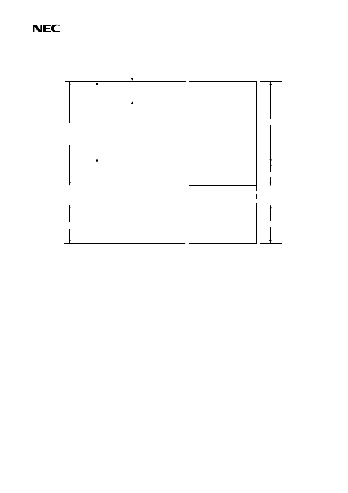
(b) µPD75106, 75104
000H
01FH
0FFH
100H
13FH
F80H
FFFH
Data memory
Memory bank
(32 × 4)
256× 4
Not provided
128× 4
Bank 0
General-purpose
register area
Stack area
General-
purpose
Static RAM
(320× 4)
Peripheral hardware area
64
× 4
Bank 1
Bank 15
Fig. 4-2 Data Memory Map(2/2)
µ
PD75104, 75106, 75108
20
5. PERIPHERAL HARDWARE FUNCTIONS
5.1 PORTS
I/O ports are classified into the following 3 kinds:
• CMOS input (PORT0, 1) : 8
• CMOS input/output (PORT2, 3, 4, 5, 6, 7, 8, 9): 32
•
N-ch open-drain input/output (PORT12, 13, 14) :12
Total : 52
PORT0
PORT1
PORT3
PORT6
PORT2
PORT4
PORT5
PORT7
PORT8
PORT9
PORT12
PORT13
PORT14
Function
4-bit input
4-bit I/O*
4-bit I/O*
(N-ch open- drain.
12V)
Table 5-1 Port Function
Operation and Features
Can always be read or tested regardless of operation mode of shared pin
Can be set in input or output mode bitwise
Can be set in input or output mode in units of 4 bits.
Ports 4 and 5, 6 and 7, 8 and 9 can be used in pairs
to input or output 8-bit data
Can be set in input or output mode in units of 4 bits.
Ports 12 and 13 can be used in pairs to input or
output 8-bit data
Port
(Symbol)
Remarks
Shared with SI, SO, SCK, and
INT0 to 4 pins
—
Port 2 pins are shared with
PTO0, PTO1, and PCL pins
Each bit can be connected to
pull-up resistor by mask option
*: Can directly drive LED.
µ
PD75104, 75106, 75108
21
5.2 CLOCK GENERATOR CIRCUIT
The clock generator circuit generates clocks to control CPU operation modes by supplying clocks to the CPU and
peripheral hardware. In addition, this circuit can change the instruction execution time.
• 0.95
µ
s/1.91 µs/15.3 µs (operating at 4.19 MHz)
· Basic interval timer (BT)
· Clock output circuit
· Timer/event counter
· Serial interface
f or
XX
f
X
1/2 1/16
1/8 to 1/4096
Frequency civider
X1
X2
System clock
generator
circuit
Oscillation
stops
Selector
1/4
Frequency
divider
· CPU
· Clock output
circuit
HALT F/F
S
RQ
PCC
PCC0
PCC1
PCC2
PCC3
4
Internal bus
HALT*
STOP*
Clears
PCC2,
PCC3
STOP F/F
Q
S
R
Wait release signal from BT
RES (internal reset) signal
Standby release signal from
interrupt control circuit
Φ
*: Execution of the instruction
Remarks 1: f
XX= Crystal/ceramic oscillator
2: f
X = External clock frequency
3: PCC: Processor clock control register
4: One clock cycle (t
CY) of Φ is one machine cycle of an instruction. For tCY, refer to AC
characteristics in 12. ELECTRICAL SPECIFICATIONS.
Fig. 5-1 Clock Generator Block Diagram
★
 Loading...