


NEC UPD75008GB-A-XXX-3B4, UPD75008GB-XXX-3B4, UPD75008CU-XXX, UPD75008CU-A-XXX, UPD75006GB-XXX-3B4 Datasheet
...
DESCRIPTION
The µPD75008 is one of the 75X Series 4-bit single-chip microcomputer.
In addition to high-speed operation with 0.95
µ
s minimum instruction execution time for the CPU, the
µ
PD75008 employs a serial bus interface with standard NEC format, the µPD75004 is a powerful product with
a high cost/performance ratio.
The µPD75P008 with PROM, which is provided with µPD75008, is applicable for evaluating systems under
development, or for small-scale production of developed systems.
Detailed functions are described in the following user’s manual. Be sure to read it for designing.
µ
PD7500X Series User’s Manual: IEM-5033
FEATURES
• Capable of high-speed operation and variable instruction execution time to power save
• 0.95
µ
s, 1.91 µs, 15.3 µs (Main system clock: operating at 4.19 MHz)
• 122
µ
s (Subsystem clock: operating at 32.768 kHz)
• 75X architecture comparable to that for an 8-bit microcomputer is employed
• Built-in NEC standard serial bus interface (SBI)
• Clock operation at reduced power dissipation (5
µ
A TYP. : operating at 3 V)
• Enhanced timer function (3 channels)
• Interrupt functions especially enhanced for applications, such as remote control receiver
APPLICATIONS
VCRs, CD players, telephones, cameras, blood pressure gauges, etc.
NEC Corporation 1990
Document No. IC-2633C
(O. D. No. IC-7673E)
Date Published November 1993 P
Printed in Japan
DATA SHEET
MOS INTEGRATED CIRCUIT
µ
PD75004, 75006, 75008
The information in this document is subject to change without notice.
4-BIT SINGLE-CHIP MICROCOMPUTER
The mark ★ shows major revised points.
Unless otherwise specified, µPD75008 is treated as the representative model throughout this manual.

µ
PD75004, 75006, 75008
2
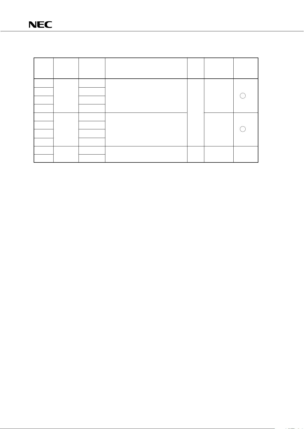
ORDERING INFORMATION
Part Number Package Quality Grade
µ
PD75004CU-xxx 42-pin plastic shrink DIP (600 mil) Standard
µ
PD75004GB-xxx-3B4 44-pin plastic QFP (■■10 mm) Standard
µ
PD75006CU-xxx 42-pin plastic shrink DIP (600 mil) Standard
µ
PD75006GB-xxx-3B4 44-pin plastic QFP (■■10 mm) Standard
µ
PD75008CU-xxx 42-pin plastic shrink DIP (600 mil) Standard
µ
PD75008GB-xxx-3B4 44-pin plastic QFP (■■10 mm) Standard
Remarks: xxx is ROM code number.
Please refer to “Quality Grade on NEC Semiconductor Devices” (Document Number IEI-1209) published by
NEC Corporation to know the specification of quality grade on the devices and its recommended applications.
µ
PD75004, 75006, 75008
3
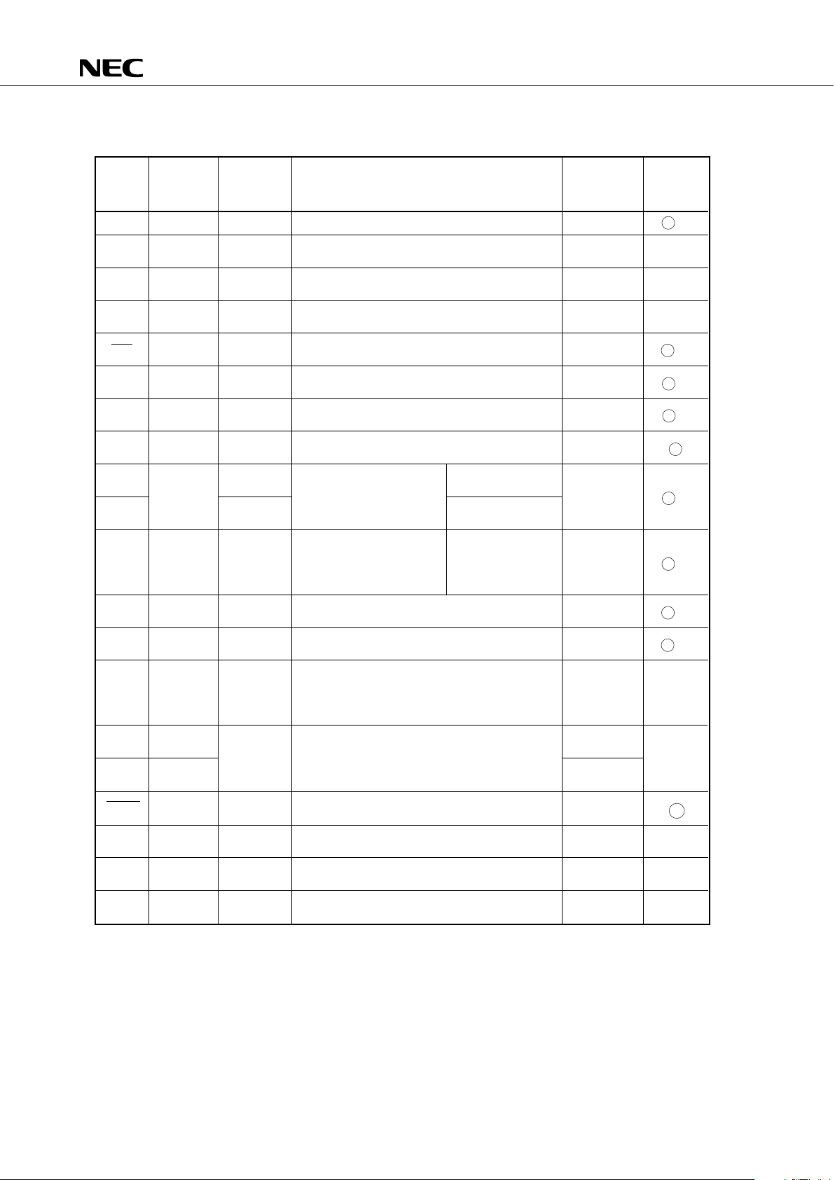
FUNCTIONAL OUTLINE
Item Function
Instruction 0.95, 1.91, and 15.3 µs, (Main system clock: operating at 4.19 MHz)
Execution Time 122 µs (Subsystem clock: operating at 32.768 kHz)
4096 × 8-bit (µPD75004)
ROM 6016 × 8-bit (µPD75006)
8064 × 8-bit (µPD75008)
RAM 512 × 4-bit
General-Purpose • 4-bit manipulation: 8
Registers • 8-bit manipulation: 4
8 CMOS Input pins Internal pull-up resistor
specification by software
18 CMOS input/output pins is possible. : 25
34 Can directly drive LED: 4
8 N-ch open-drain Withstand voltage: 10V
input/output Internal pull-up resistor
Can directly drive LED: 8 specification by mask option
is possible.
Timer/event counter
Timer 3 chs Basic interval timer: Also serves as watchdog timer
Watch timer: Buzzer output possible
Serial 3-line serial I/O mode
Interface 2-line serial I/O mode
SBI mode
Bit Sequential 16 bits
Buffer
Clock Output Function Φ, fx/23, fx/24, fx/2
6
Vector Interrupt External: 3, Internal: 3
Test Input External: 1, Internal: 1
System Clock Main system clock oscillation ceramic/crystal oscillator
Oscillator Subsystem clock oscillation crysal ocillator
Standby Function STOP/HALT mode
Operating –40 to +85°C
Temperature Range
Operating Supply 2.7 to 6.0 V
Voltage
Package 42-pin plastic shrink DIP (600 mil)
44-pin plastic QFP (■■10 mm)
Internal
Memory
I/O Port

µ
PD75004, 75006, 75008
4
CONTENTS
1. PIN CONFIGURATION (TOP VIEW)............................................................................................... 6
2. BLOCK DIAGRAM ........................................................................................................................... 8
3. PIN FUNCTIONS.............................................................................................................................. 9
3.1 PORT PINS............................................................................................................................................. 9
3.2 NON PORT PINS................................................................................................................................... 11
3.3 PIN INPUT/OUTPUT CIRCUITS ........................................................................................................... 12
3.4 SELECTION OF MASK OPTION .......................................................................................................... 14
3.5 RECOMMENDED PROCESSING OF UNUSED PINS.......................................................................... 14
3.6 NOTES ON USING THE P00/INT4, AND RESET PINS...................................................................... 15
4. MEMORY CONFIGURATION .......................................................................................................... 16
5. PERIPHERAL HARDWARE FUNCTIONS........................................................................................ 20
5.1 PORTS .................................................................................................................................................... 20
5.2 CLOCK GENERATOR CIRCUIT ............................................................................................................ 21
5.3 CLOCK OUTPUT CIRCUIT.................................................................................................................... 22
5.4 BASIC INTERVAL TIMER ..................................................................................................................... 23
5.5 WATCH TIMER ...................................................................................................................................... 24
5.6 TIMER/EVENT COUNTER ..................................................................................................................... 24
5.7 SERIAL INTERFACE .............................................................................................................................. 26
5.8 BIT SEQUENTIAL BUFFER................................................................................................................... 28
6. INTERRUPT FUNCTIONS................................................................................................................ 28
7. STANDBY FUNCTIONS .................................................................................................................. 30
8. RESET FUNCTION........................................................................................................................... 31
9. INSTRUCTION SET ......................................................................................................................... 33
10. ELECTRICAL SPECIFICATIONS ...................................................................................................... 40
11. CHARACTERISTIC CURVES ........................................................................................................... 53

µ
PD75004, 75006, 75008
5
12. PACKAGE DRAWINGS ................................................................................................................... 58
13. RECOMMENDED SOLDERING CONDITIONS ............................................................................... 61
APPENDIX A. DEVELOPMENT TOOLS .............................................................................................. 62
APPENDIX B. RELATED DOCUMENTS .............................................................................................. 63
µ
PD75004, 75006, 75008
6
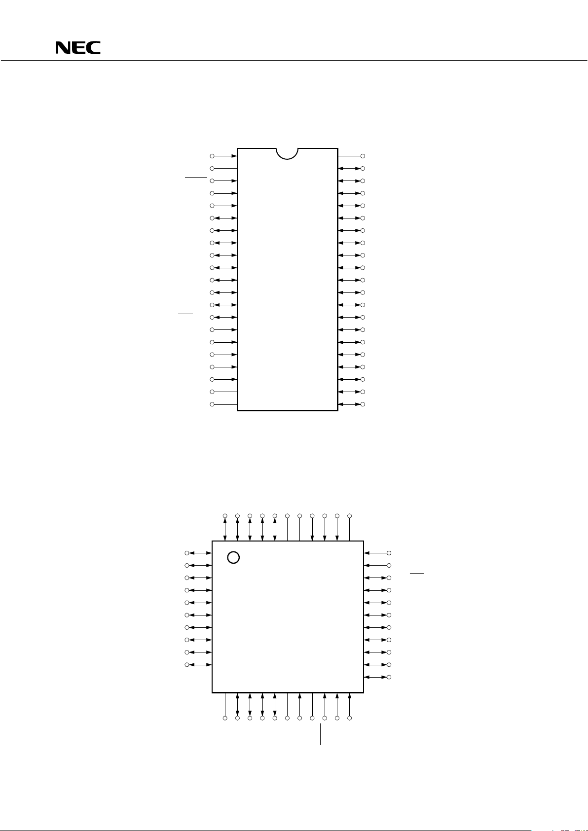
1. PIN CONFIGURATION (Top View)
• 42-pin plastic shrink DIP (600 mil)
P72/KR6
NC
P03/TI0
P73/KR7
PD75004GB–xxx–3B4
µ
P20/PTO0
P21
P22/PCL
P23/BUZVNC
P10/INT0
P11/INT1
P12/INT2
NC
P43
P42
P40
V
XT1
XT2
RESET
X1
X2
1
44 43 42 41 40 39 38 37 36 35 34
12 13 14 15 16 17 18 19 20 21 22
P71/KR5
P70/KR4
P63/KR3
P62/KR2
P61/KR1
P60/KR0
P53
P52
P51
P50
2
3
4
5
6
7
8
9
10
11
33
32
31
30
29
28
27
26
25
24
23
P00/INT4
P01/SCK
P02/SO/SB0
P03/SI/SB1
P80
P81
P30
P31
P32
P33
P41
DD
SS
PD75006GB–xxx–3B4
µ
PD75008GB–xxx–3B4
µ
XT1
V
PD75004CU-xxx
µ
1
XT2
RESET
X1
X2
P33
P32
P31
P30
P81
P80
SI/SB1/P03
SO/SB0/P02
SCK/P01
INT4/P00
TI0/P13
INT2/P12
INT1/P11
INT0/P10
NC
2
3
4
5
6
7
8
9
10
11
12
13
14
15
16
17
18
19
20
42
41
40
39
38
37
36
35
34
33
32
31
30
29
28
27
26
25
24
23
P40
P41
P42
P43
P50
P51
P52
P53
P60/KR0
P61/KR1
P62/KR2
P63/KR3
P70/KR4
P71/KR5
P72/KR6
P73/KR7
P20/PTO0
P21
P22/PCL
21 22
SS
P23/BUZ
PD75006CU-xxx
µ
PD75008CU-xxx
µ
VDD
• 44-pin plastic QFP (■■ 10 mm)

µ
PD75004, 75006, 75008
7
Pin names
P00-P03 : Port 0 SO : Serial Output
P10-P13 : Port 1 SB0,SB1 : Serial Bus 0,1
P20-P23 : Port 2 RESET : Reset Input
P30-P33 : Port 3 TI0 : Timer Input 0
P40-P43 : Port 4 PTO0 : Programmable Timer Output 0
P50-P53 : Port 5 BUZ : Buzzer Clock
P60-P63 : Port 6 PCL : Programmable Clock
P70-P73 : Port 7 INT0, 1, 4 : External Test Interrupt 0,1,4
P80-P81 : Port 8 INT2 : External Test Input 2
KR0-KR7 : Key Return X1, 2 : Main System Clock Oscillation 1,2
SCK : Serial Clock XT1, 2 : Subsystem Clock Oscillation 1,2
SI : Serial Input NC : No Connection
µ
PD75004, 75006, 75008
8
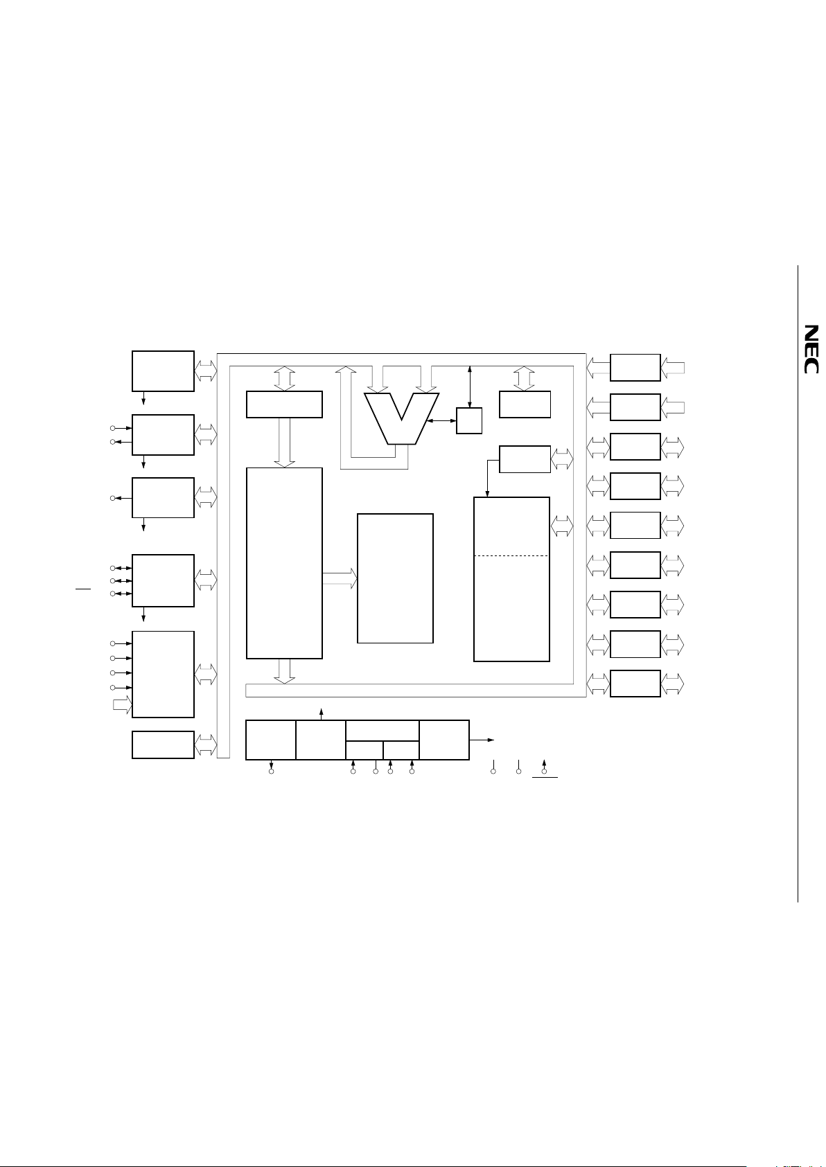
2. BLOCK DIAGRAM
TI0/P13
BASIC
INTERVAL
TIMER
INTBT
TIMER/EVENT
COUNTER
#0
INTT0
PTO0/P20
BUZ/P23
WATCH
TIMER
INTW
INTCSI
CLOCKED
SERIAL
INTERFACE
SI/SB1/P03
SO/SB0/P02
SCK/P01
PROGRAM
COUNTER *
ALU
CY
SP (8)
BANK
INT0/P10
INT1/P11
INT2/P12
INT4/P00
KR0/P60
–KR7/P73
INTERRUPT
CONTROL
BIT SEQ.
BUFFER (16)
PROGRAM
MEMORY
(ROM)
4096 8 BITS
( PD75004)
6016 8 BITS
( PD75006)
8064 8 BITS
( PD75008)
×
DECODE
AND
CONTROL
GENERAL REG.
DATA
MEMORY
(RAM)
512 4 BITS
×
f /2
X
N
V DD V SS RESET
PCL/P22 XT1 XT2 X1 X2
SUB MAIN
CLOCK
OUTPUT
CONTROL
CLOCK
DIVIDER
SYSTEM CLOCK
GENERATOR
STAND BY
CONTROL
CPU
CLOCK
PORT 8
P80-P812
PORT 6
P60-P634
PORT 5
P50-P534
PORT 4
P40-P434
PORT 3
P30-P33
4
PORT 2
P20-P234
PORT 1
P10-P134
PORT 0
P00-P034
×
µ
µ
PORT 7
P70-P734
×
µ
*: For PD75004, 12 bits. For PD75006 and PD75008, 13 bits.
µµµ
µ
PD75004, 75006, 75008
9
3. PIN FUNCTIONS
3.1 PORT PINS (1/2)
Input/
Output
Circuit
TYPE*
1
P00
P01
P02
P03
P10
P11
P12
P13
P20
P21
P22
P23
P30*
2
P31*
2
P32*
2
P33*
2
P40-43*
2
P50-53*
2
Pin Name
Input/Output Function 8-Bit I/O When Reset
Also Served
As
INT4
SCK
SO/SB0
SO/SB1
INT0
INT1
INT2
TI0
PTO0
—
PCL
BUZ
—
—
—
—
—
—
4-bit input port (PORT0)
Pull-up resistors can be specified in 3-bit
units for the P01 to P03 pins by software.
With noise elimination function
4-bit input port (PORT1)
Internal pull-up resistors can be
specified in 4-bit units by software.
4-bit input/output port (PORT2)
Internal pull-up resistors can be
specified in 4-bit units by software.
Programmable 4-bit input/output port
(PORT3)
This port can be specified for input/
output in bit units.
Internal pull-up resistors can be
specified in 4-bit units by software.
N-ch open-drain 4-bit input/output port
(PORT4)
Internal pull-up resistors can be
specified in bit units. (mask option)
Resistive voltage is 10 V in the opendrain mode.
N-ch open-drain 4-bit input/output port
(PORT5)
Internal pull-up resistors can be
specified in bit units. (mask option)
Resistive voltage is 10 V in the opendrain mode.
Input
Input
Input
Input
High level
(with internal
pull-up
resistor) or
high impedance
B
B -C
E-B
E-B
M
M
X
X
X
X
*1: Circles indicate Schmitt trigger inputs.
2: Can directly drive LED.
Input
Input/
Output
Input/
Output
Input/
Output
Input
Input/
Output
Input/
Output
Input/
Output
Input/
Output
●●
F -A
M -C
F -B
High level
(with internal
pull-up
resistor) or
high impedance
µ
PD75004, 75006, 75008
10
P60
P61
P62
P63
P70
P71
P72
P73
P80
P81
KR0
KR1
KR2
KR3
KR4
KR5
KR6
KR7
—
—
●●
Input/
Output
Input/
Output
Input/
Output
Also Served
As
3.1 PORT PINS (2/2)
Input/
Output
Circuit
TYPE*
1
Programmable 4-bit input/output port
(PORT6)
This port can be specified for input/
output in bit units.
Internal pull-up resistors can be
specified in 4-bit units by software.
Input
F -A
4-bit input/output port (PORT7)
Internal pull-up resistors can be
specified in 4-bit units by software.
Input
F -A
Pin Name Input/Output Function 8-Bit I/O When Reset
2-bit input/output port (PORT8)
Internal pull-up resistors can be
specified in 2-bit units by software.
X
Input
E-B
*1: Circles indicate Schmitt trigger inputs.
2: Can directly drive LED.
µ
PD75004, 75006, 75008
11
TI0
PTO0
PCL
BUZ
SCK
SO/SB0
SI/SB1
INT4
INT0
INT1
INT2
KR0-KR3
KR4-KR7
P13
P20
P22
P23
P01
P02
P03
P00
P10
P11
P12
P60-P63
P70-P73
Input
Input
Input
Input
Input
Input
Input
Input
Input
Input
Input
Input
B -C
E-B
E-B
E-B
F -A
F -B
M -C
B
B -C
B -C
F -A
F -A
Pin Name Input/Output
Also Served
As
Functon When Reset
Input/
Output
Circuit
TYPE*
1
3.2 NON PORT PINS
Timer/event counter external event pulse Input
Timer/event counter output
Clock output
Fixed frequency output (for buzzer or for trimming the system clock)
Serial clock input/output
Serial data output
Serial bus input/output
Serial data input
Serial bus input/output
Edge detection vector interrupt input (both
rising and falling edge detection are effective)
Edge detection vector
interrupt input (detection
edge can be selected)
Edge detection testable
input (rising edge detection)
Clock synchronous
Asynchronous
Asynchronous
X1, X2
RESET
NC *
2
VDD
VSS
Input
—
Input
—
—
—
—
—
—
—
B
—
—
—
—
—
—
—
Input —
—
*1: Circles indicate Schmitt trigger inputs.
2: When sharing the printed circut board with the
µ
PD75P008, the NC pin must be directly
connected to V
DD.
Input
Input/
Output
Input/
Output
Input/
Output
Input/
Output
Input/
Output
Input/
Output
Input
Input
Input
Input/
Output
Input/
Output
XT1
XT2
—
Input
—
Input
—
Parallel falling edge detection testable input
Parallel falling edge detection testable input
To connect the crystal/ceramic oscillator to the
main system clock generator. When inputting the
external clock, input the external clock to pin X1,
and the reverse phase of the external clock to pin
X2.
To connect the crystal oscillator to the subsystem
clock generator.
When the external clock is used, pin XT1 inputs
the external clock. In this case, pin XT2 must be
left open.
System reset input
No connection
Positive power supply
GND
µ
PD75004, 75006, 75008
12
3.3 PIN INPUT/OUTPUT CIRCUITS
The following shows a simplified input/output circuit diagram for each pin of the
µ
PD75008.
TYPE A (for TYPE E–B)
TYPE D (for TYPE E –B, F
TYPE B
TYPE E–B
IN
V
DD
Input buffer of CMOS standard
data
output
disable
OUT
P–ch
N–ch
Push–pull output that can be set in a output
high–impedance state (both P–ch and N–ch are off)
IN
Schmitt trigger input with hysteresis characteristics
data
output
disable
Type D
Type A
P.U.R.
enable
V
DD
P.U.R.
P–ch
IN/OUT
P.U.R. : Pull–Up Resistor
P.U.R.
enable
V
DD
P.U.R.
P–ch
TYPE B–C
TYPE F–A
IN
data
output
disable
Type D
Type B
P.U.R.
enable
V
DD
P.U.R.
P–ch
IN/OUT
P.U.R. : Pull–Up ResistorP.U.R. : Pull
–Up Resistor
A)–
V
DD
µ
PD75004, 75006, 75008
13
TYPE M–C
TYPE F–B
data
output
disable
P.U.R.
enable
V
DD
IN/OUT
Middle voltage input buffer
(withstand voltage: +10 V)
P.U.R. : Pull–Up Resistor
data
output
disable
P.U.R.
enable
V
DD
P.U.R.
P–ch
N-ch
P-ch
output
disable
(P)
output
disable
(N)
V
DD
(Mask option)
P.U.R. : Pull–Up Resistor
IN/OUT
data
output
disable
P.U.R.
enable
V
DD
P.U.R.
IN/OUT
P–ch
N-ch
P.U.R. : Pull–Up Resistor
N-ch
(withstand
voltage:
+10 V)
TYPE M
µ
PD75004, 75006, 75008
14
3.4 SELECTION OF MASK OPTION
The following mask operations are available and can be specified for each pin.
Table 3-1 Mask Option Selection
Pin Mask Option
P40-P43,
P50-P53
• With pull-up resistor
• Without pull-up resistor
*: Mask option can be specified in bit units.
3.5 RECOMMENDED PROCESSING OF UNUSED PINS
Table 3-2 Processing of Unused Pins
Pin Recommended Connections
P00/INT4 Connect to VSS
P01/SCK
P02/SO/SB0 Connect to VSS or VDD
P03/SI/SB1
P10/INT0-P12/INT2
P13/TI0
P20/PTO0
P21
P22/PCL
P23/BUZ
P30-P33 Input : Connect to VSS or VDD
P40-P43 Output: Open
P50-P53
P60-P63
P70-P73
P80-P81
XT1 Connect to VSS or VDD
XT2 Open
Connect to VSS
★
µ
PD75004, 75006, 75008
15
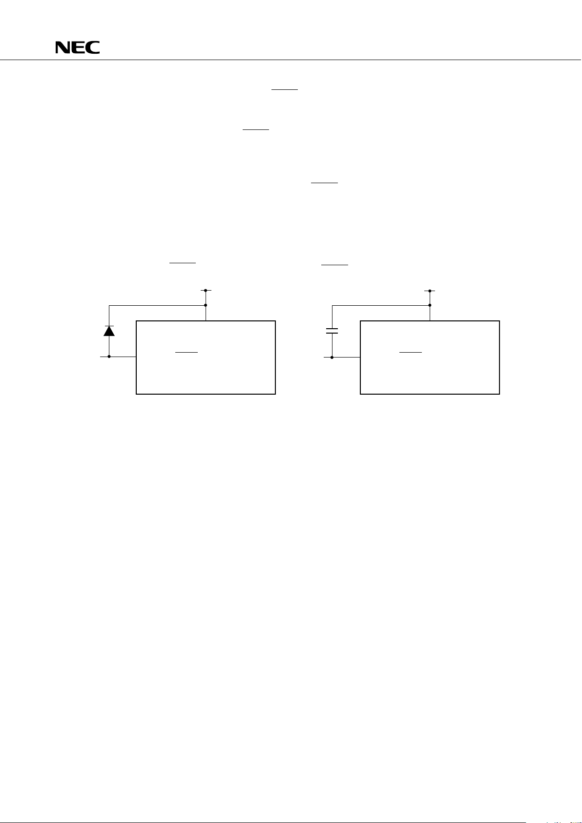
3.6 NOTES ON USING THE P00/INT4, AND RESET PINS
In addition to the functions described in Sections 3.1 PORT PINS and 3.2 NON PORT PINS, an exclusive
function for setting the test mode, in which the internal fuctions of the
µ
PD75008 are tested (solely used for
IC tests), is provided to the P00/INT4 and
RESET
pins.
If a voltage exceeding V
DD is applied to either of these pins, the
µ
PD75008 is put into test mode. Therefore,
even when the
µ
PD75008 is in normal operation, if noise exceeding the VDD is input into any of these pins, the
µ
PD75008 will enter the test mode, and this will cause problems for normal operation.
As an example, if the wiring to the P00/INT4 pin or the
RESET
pin is long, stray noise may be picked up
and the above montioned problem may occur.
Therefore, all wiring to these pins must be made short enough to not pick up stray noise. If noise cannot
be avoided, suppress the noise using a capacitor or diode as shown in the figure below.
• Connect a capacitor across P00/INT4 and
RESET, and V
DD.
VDD
VDD
P00/INT4, RESET
VDD
VDD
P00/INT4, RESET
Low VF
diode
• Connect a diode having a low VF across
P00/INT4 and RESET, and V
DD. (0.3 V max.)
★

µ
PD75004, 75006, 75008
16
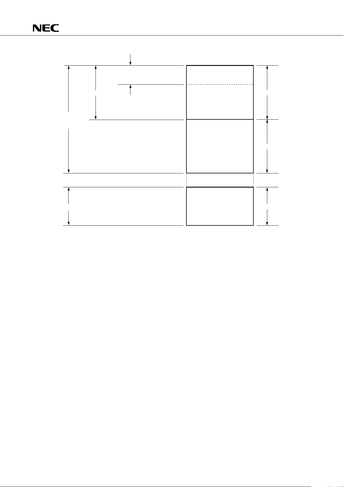
4. MEMORY CONFIGURATION
• Program memory (ROM) ... 4096 × 8 bits (0000H-0FFFH) :
µ
PD75004
... 6016 × 8 bits (0000H-177FH) :
µ
PD75006
... 8064 × 8 bits (0000H-1F7FH) :
µ
PD75008
• 0000H-0001H: Vector table to which address from which program is started is written after reset
• 0002H-000BH: Vector table to which address from which program is started is written after interrupt
• 0020H-007FH: Table area referenced by GETI instruction
• Data memory (RAM)
• Data area .... 512 × 4 bits (000H–1FFH)
• Peripheral hardware area .... 128 × 4 bits (F80H–FFFH)
765
MBE 0 0
MBE 0 0
MBE 0 0
MBE 0 0
MBE 0 0
MBE 0 0
Internal reset start address (upper 4 bits)
Internal reset start address (lower 8 bits)
INTBT/INT4 start address (upper 4 bits)
INTBT/INT4 start address (lower 8 bits)
INT0 start address (upper 4 bits)
INT0 start address (lower 8 bits)
INT1 start address (upper 4 bits)
INT1 start address (lower 8 bits)
INTCSI start address (upper 4 bits)
INTCSI start address (lower 8 bits)
INTT0 start address (upper 4 bits)
INTT0 start address (lower 8 bits)
000H
002H
004H
006H
008H
00AH
020H
07FH
080H
7FFH
800H
FFFH
GETI instruction reference table
0
CALLF
!faddr
instruction
entry
address
BRCD ! caddr
instruction
branch address
CALL ! addr
instruction
subroutine
entry address
BR $addr
instruction
relational
branch address
(–15 to –1,
+2 to +16)
Branch destination
address and
subroutine entry
address for
GETI instruction
Address
4
0
0
0
0
0
0
Fig. 4-1 Program Memory Map (µPD75004)
µ
PD75004, 75006, 75008
17
765
MBE 0 0
MBE 0 0
MBE 0 0
MBE 0 0
MBE 0 0
MBE 0 0
Internal reset start address (upper 5 bits)
Internal reset start address (lower 8 bits)
INTBT/INT4 start address (upper 5 bits)
INTBT/INT4 start address (lower 8 bits)
INT0 start address (upper 5 bits)
INT0 start address (lower 8 bits)
INT1 start address (upper 5 bits)
INT1 start address (lower 8 bits)
INTCSI start address (upper 5 bits)
INTCSI start address (lower 8 bits)
INTT0 start address (upper 5 bits)
INTT0 start address (lower 8 bits)
0000H
0002H
0004H
0006H
0008H
000AH
0020H
007FH
0080H
07FFH
0800H
0FFFH
1000H
177FH
GETI instruction reference table
0
BRCB
! caddr
instruction
branch
address
CALLF
! faddr
instruction
entry
address
BR ! addr
instruction
branch address
CALL ! addr
instruction
subroutine
entry address
BR $addr
instruction
relational
branch address
(–15 to –1,
+2 to +16)
Branch destination
address and
subroutine entry
address for
GETI instruction
Address
BRCB ! caddr
instruction
branch address
Fig. 4-2 Program Memory Map (µPD75006)
µ
PD75004, 75006, 75008
18
765
MBE 0 0
MBE 0 0
MBE 0 0
MBE 0 0
MBE 0 0
MBE 0 0
Internal reset start address (upper 5 bits)
Internal reset start address (lower 8 bits)
INTBT/INT4 start address (upper 5 bits)
INTBT/INT4 start address (lower 8 bits)
INT0 start address (upper 5 bits)
INT0 start address (lower 8 bits)
INT1 start address (upper 5 bits)
INT1 start address (lower 8 bits)
INTCSI start address (upper 5 bits)
INTCSI start address (lower 8 bits)
INTT0 start address (upper 5 bits)
INTT0 start address (lower 8 bits)
0000H
0002H
0004H
0006H
0008H
000AH
0020H
007FH
0080H
07FFH
0800H
0FFFH
1000H
1F7FH
GETI instruction reference table
0
BRCB
! caddr
instruction
branch
address
CALLF
! faddr
instruction
entry
address
BR ! addr
instruction
branch address
CALL ! addr
instruction
subroutine
entry address
BR $addr
instruction
relational
branch address
(–15 to –1,
+2 to +16)
Branch destination
address and
subroutine entry
address for
GETI instruction
Address
BRCB ! caddr
instruction
branch address
Fig. 4-3 Program Memory Map (µPD75008)
µ
PD75004, 75006, 75008
19
000H
007H
008H
0FFH
100H
1FFH
F80H
FFFH
Data memory
Memory bank
(8 × 4)
256× 4
(248× 4)
Not provided
128× 4
0
1
15
General-purpose
register area
Stack area
Data area
Static RAM
(512× 4)
Peripheral hardware area
256× 4
Fig. 4-4 Data Memory Map
µ
PD75004, 75006, 75008
20
5. PERIPHERAL HARDWARE FUNCTIONS
5.1 PORTS
I/O ports are classified into the following 3 kinds:
• CMOS input (PORT0, 1) : 8
• CMOS input/output (PORT2, 3, 6, 7, and 8) : 18
• N-ch open-drain input/output (PORT4, 5) : 8
Total : 34
Remarks
Multiplexed with SO/SB0,
SI/SB1, SCK, INT0-2, 4,
and TIO
Port 6 is multiplexed with
KR0 to KR3.
Port 2 is multiplexed with
PTO0, PCL, and BUZ.
Port 7 is multiplexed with
KR4-KR7.
Can be connected to a
pull-up resistor in 1-bit
units by using mask
option.
—
PORT0
PORT1
PORT3*
PORT6
PORT2
PORT7
PORT4*
PORT5*
PORT8
Function
4-bit input
4-bit input/output
4-bit input/output
(N-ch open-drain,
10 V)
2-bit input/output
Table 5-1 Port Function
Operation and Feature
Can be always read or tested regardless of operation mode of multiplexed pin.
Can be set in input or output mode in 1-bit units.
Can be set in input or output mode in 4-bit units.
Ports 6 and 7 are used in pairs to input/output data
in 8-bit units.
Can be set in input or output mode in 4-bit units.
Ports 4 and 5 are used in pairs to input/output data
in 8-bit units.
Can be set input or output mode in 2-bit units.
*: Can directly drive LED.
Port Name
(Symbol)
 Loading...