


NEC UPD70216HLP-20, UPD70216HLP-16, UPD70208HLP-10, UPD70208HLP-12, UPD70208HGK-20-9EU Datasheet
...
DATA SHEET
MOS INTEGRATED CIRCUIT
µ
PD70208H, 70216H
V40HLTM, V50HL
TM
16/8, 16-BIT MICROPROCESSOR
DESCRIPTION
The µPD70208H (V40HL) is a high-speed, low-power 16-/8-bit microprocessor based on the µPD70208 (V40TM) with
16-bit architecture, 8-bit data bus, and general-purpose peripheral functions.
µ
PD70216H (V50HL) is a high-speed, low-power 16-bit microprocessor based on the µPD70216 (V50TM) with 16-
The
bit architecture, 16-bit data bus, and general-purpose peripheral functions.
The V40HL and V50HL offer 20 MHz operation, and in addition to the conventional standby functions, also allows the
clock to be stopped by the use of fully static internal circuitry, thus achieving greatly reduced power consumption. It is also
capable of 3 V operation in addition to the previous 5 V operation, making it ideally suited to battery driven systems.
Details are given in the following manuals. Be sure to read when carrying out design work.
• V40HL, V50HL User’s Manual – Hardware (U11610E)
TM
• 16-bit V series
FEATURES
User’s Manual – Instruction (U11301J: Japanese version)
• High-speed, low-power version of V40 and V50
• High-performance CPU (V20
• Minimum instruction execution time: 100 ns (20 MHz, 5 V)
• Memory addressing space: 1M bytes
• High-speed multiply/divide instructions: 0.95 to 2.8
• Maskable (ICU) & non-maskable (NMI) interrupt inputs
•µPD8080AF emulation function
• Standby functions, clock stoppage capability
TM
/V30TM software compatible)
200 ns (10 MHz, 3 V)
1.9 to 5.6 µs (10 MHz, 3 V)
µ
s (20 MHz, 5 V)
• Standard peripheral LSI functions on chip
• Clock generator (CG)
• Programmable wait control unit (WCU)
• Refresh control unit (REFU)
µ
• Timer/counter unit (TCU) ···
• Serial control unit (SCU) ··· µPD71051 subset
• Interrupt control unit (ICU) ··· µPD71059 subset
• DMA control unit (DMAU) ··· µPD71071/71037 subset (functions of either selectable)
PD71054 subset
• Operating frequency: 10/12.5/16/20 MHz (at 5 V, with 20/25/32/40 MHz supplied externally)
5/6.25/8/10 MHz (at 3 V, with 10/12.5/16/20 MHz supplied externally)
The information in this document is subject to change without notice. Before using this document, please
confirm that this is the latest version.
Not all devices/types available in every country. Please check with local NEC representative for availability
and additional information.
Document No. U13225EJ4V0DS00 (4th edition)
Date Published April 1999 N CP(K)
Printed in Japan
The mark shows the the major revised points.
©
1995

µ
PD70208H, 70216H
ORDERING INFORMATION
(1) V40HL
Part Number Package Frequency (MHz)
µ
PD70208HGF-10-3B9 80-pin plastic QFP (14 × 20 mm) 10
(Resin thickness 2.7 mm)
µ
PD70208HGF-12-3B9 80-pin plastic QFP (14 × 20 mm) 12.5
(Resin thickness 2.7 mm)
µ
PD70208HGF-16-3B9 80-pin plastic QFP (14 × 20 mm) 16
(Resin thickness 2.7 mm)
µ
PD70208HGF-20-3B9 80-pin plastic QFP (14 × 20 mm) 20
(Resin thickness 2.7 mm)
µ
PD70208HGK-10-9EU 80-pin plastic TQFP (Fine pitch) (12 × 12 mm) 10
(Resin thickness 1.0 mm)
µ
PD70208HGK-12-9EU 80-pin plastic TQFP (Fine pitch) (12 × 12 mm) 12.5
(Resin thickness 1.0 mm)
µ
PD70208HGK-16-9EU 80-pin plastic TQFP (Fine pitch) (12 × 12 mm) 16
(Resin thickness 1.0 mm)
µ
PD70208HGK-20-9EU 80-pin plastic TQFP (Fine pitch) (12 × 12 mm) 20
(Resin thickness 1.0 mm)
µ
PD70208HLP-10 68-pin plastic QFJ (950 × 950 mil) 10
µ
PD70208HLP-12 68-pin plastic QFJ (950 × 950 mil) 12.5
µ
PD70208HLP-16 68-pin plastic QFJ (950 × 950 mil) 16
µ
PD70208HLP-20 68-pin plastic QFJ (950 × 950 mil) 20
Max. Operating
(2) V50HL
Part Number Package Frequency (MHz)
µ
PD70216HGF-10-3B9 80-pin plastic QFP (14 × 20 mm) 10
(Resin thickness 2.7 mm)
µ
PD70216HGF-12-3B9 80-pin plastic QFP (14 × 20 mm) 12.5
(Resin thickness 2.7 mm)
µ
PD70216HGF-16-3B9 80-pin plastic QFP (14 × 20 mm) 16
(Resin thickness 2.7 mm)
µ
PD70216HGF-20-3B9 80-pin plastic QFP (14 × 20 mm) 20
(Resin thickness 2.7 mm)
µ
PD70216HGK-10-9EU 80-pin plastic TQFP (Fine pitch) (12 × 12 mm) 10
(Resin thickness 1.0 mm)
µ
PD70216HGK-12-9EU 80-pin plastic TQFP (Fine pitch) (12 × 12 mm) 12.5
(Resin thickness 1.0 mm)
µ
PD70216HGK-16-9EU 80-pin plastic TQFP (Fine pitch) (12 × 12 mm) 16
(Resin thickness 1.0 mm)
µ
PD70216HGK-20-9EU 80-pin plastic TQFP (Fine pitch) (12 × 12 mm) 20
(Resin thickness 1.0 mm)
µ
PD70216HLP-10 68-pin plastic QFJ (950 × 950 mil) 10
µ
PD70216HLP-12 68-pin plastic QFJ (950 × 950 mil) 12.5
µ
PD70216HLP-16 68-pin plastic QFJ (950 × 950 mil) 16
µ
PD70216HLP-20 68-pin plastic QFJ (950 × 950 mil) 20
Max. Operating
2
Data Sheet U13225EJ4V0DS00
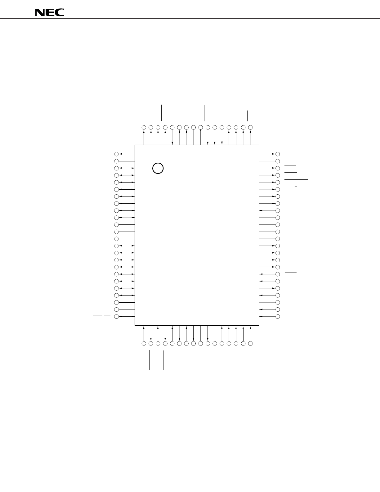
PIN CONFIGURATION (Top View)
(1) V40HL
• 80-pin Plastic QFP (14 × 20 mm)
µ
PD70208HGF-10-3B9
µ
PD70208HGF-12-3B9
µ
PD70208HGF-16-3B9
µ
PD70208HGF-20-3B9
A17/PS1
A18/PS2
A19/PS3
REFRQ
HLDRQ
HLDAK
RESOUT
VDDVDDRESET
READY
NMI
BS2
BS1
µ
PD70208H, 70216H
BS0
MRD
A16/PS0
NC
A15
A14
A13
A12
A11
A10
A9
A8
GND
NC
GND
AD7
AD6
AD5
AD4
AD3
AD2
AD1
AD0
NC
NC
END/TC
80 79 78 77 76 75 74 73 72 71 70 69 68 67 66 65
1
2
3
4
5
6
7
8
9
10
11
12
13
14
15
16
17
18
19
20
21
22
23
24
25 26 27 28 29 30 31 32 33 34 35 36 37 38 39 40
64
63
62
61
60
59
58
57
56
55
54
53
52
51
50
49
48
47
46
45
44
43
42
41
IORD
NC
MWR
IOWR
BUSLOCK
BUFR/W
BUFEN
CLKOUT
X1
X2
GND
NC
GND
High
ASTB
QS0
QS1
POLL
TCTL2
TOUT2
TCLK
NC
INTP7
INTP6
D
D
IC
X
X
DMAAK1
DMARQ0
DMARQ1
DMAAK0
DMAAK2
DMARQ2
DMARQ3/R
DMAAK3/T
INTAK/SRDY/TOUT1
Caution Leave IC pin open.
Data Sheet U13225EJ4V0DS00
DD
V
INTP1
INTP2
INTP3
INTP4
INTP5
3
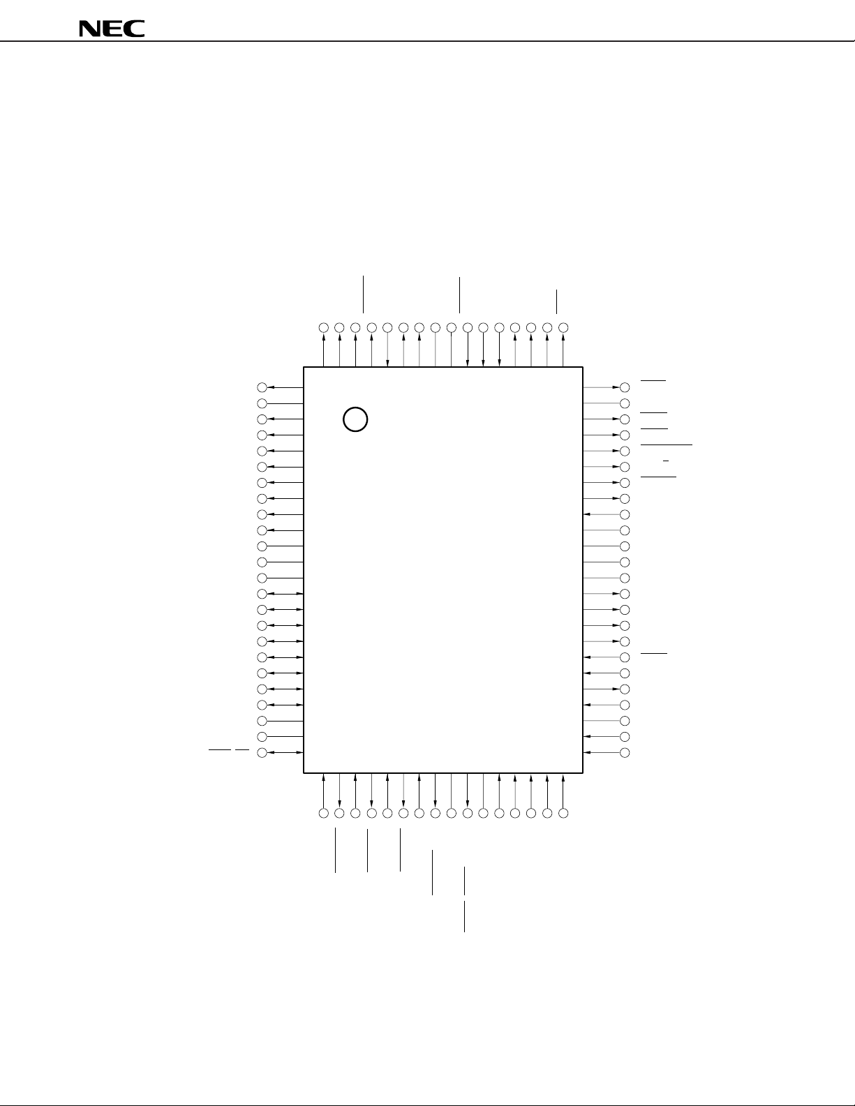
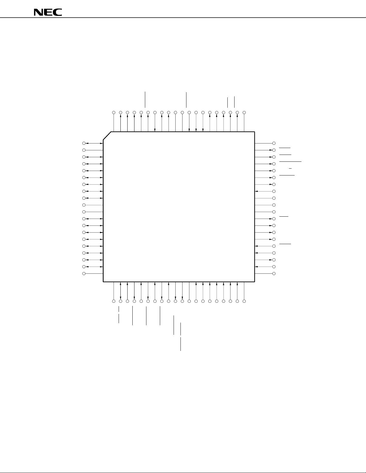
• 80-pin Plastic TQFP (Fine pitch) (12 × 12 mm)
µ
PD70208HGK-10-9EU
µ
PD70208HGK-12-9EU
µ
PD70208HGK-16-9EU
µ
PD70208HGK-20-9EU
NC
A16/PS0
A17/PS1
A18/PS2
A19/PS3
REFRQ
HLDRQ
HLDAK
80 79 78 77 76 75 74 73 72 71 70 69 68 67 66 65 64 63 62 61
A15
NC
A14
A13
A12
A11
A10
A9
A8
GND
GND
AD7
AD6
AD5
AD4
AD3
AD2
AD1
AD0
NC
1
2
3
4
5
6
7
8
9
10
11
12
13
14
15
16
17
18
19
20
21 22 23 24 25 26 27 28 29 30 31 32 33 34 35 36 37 38 39 40
RESOUT
VDDVDDRESET
READY
NMI
BS2
BS1
BS0
MRD
µ
PD70208H, 70216H
IORD
NC
60
59
58
57
56
55
54
53
52
51
50
49
48
47
46
45
44
43
42
41
NC
MWR
IOWR
BUSLOCK
BUFR/W
BUFEN
CLKOUT
X1
X2
GND
GND
High
ASTB
QS0
QS1
POLL
TCTL2
TOUT2
TCLK
NC
D
D
NC
END/TC
DMARQ0
4
DMAAK1
DMARQ1
DMAAK0
Data Sheet U13225EJ4V0DS00
X
DMAAK2
DMARQ2
DMARQ3/R
DD
X
V
INTP1
INTP2
DMAAK3/T
INTAK/SRDY/TOUT1
INTP3
INTP4
INTP5
INTP6
NC
INTP7
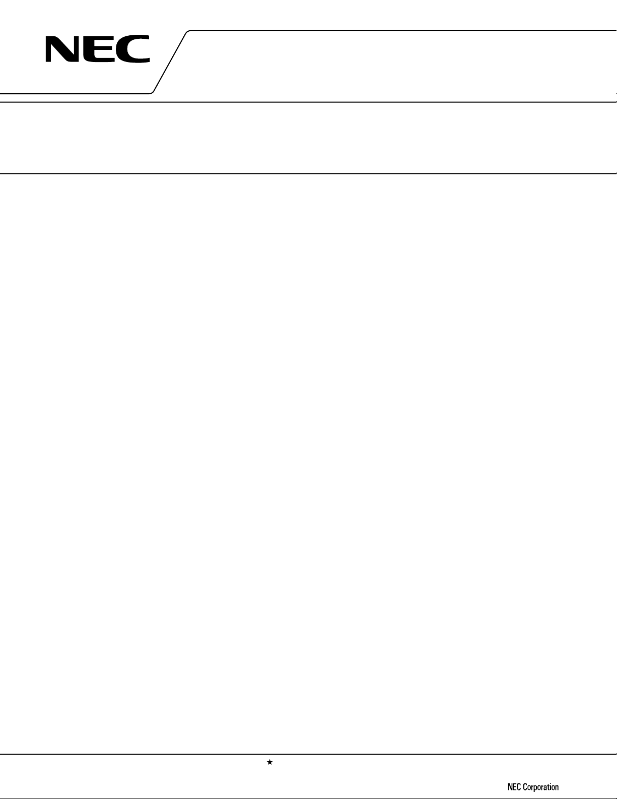
• 68-pin Plastic QFJ (950 × 950 mil)
µ
PD70208HLP-10
µ
PD70208HLP-12
µ
PD70208HLP-16
µ
PD70208HLP-20
A16/PS0
A17/PS1
A18/PS2
A19/PS3
REFRQ
HLDRQ
HLDAK
RESOUT
VDDRESET
READY
NMI
BS2
BS1
BS0
µ
PD70208H, 70216H
MRD
IORD
A15
A14
A13
A12
A11
A10
A9
A8
GND
AD7
AD6
AD5
AD4
AD3
AD2
AD1
AD0
9 8 7 6 5 4 3 2 1 68 67 66 65 64 63 62 61
10
11
12
13
14
15
16
17
18
19
20
21
22
23
24
25
26
27
28 29 30 31 32 33 34 35 36 37 38 39 40 41 42 43
XD
XD
INTP1
INTP2
END/TC
DMARQ0
DMAAK1
DMARQ1
DMAAK0
DMAAK2
DMARQ2
DMARQ3/R
DMAAK3/T
INTP3
INTP4
INTP5
60
59
58
57
56
55
54
53
52
51
50
49
48
47
46
45
44
INTP6
INTP7
MWR
IOWR
BUSLOCK
BUFR/W
BUFEN
CLKOUT
X1
X2
GND
High
ASTB
QS0
QS1
POLL
TCTL2
TOUT2
TCLK
INTAK/SRDY/TOUT1
Data Sheet U13225EJ4V0DS00
5
(2) V50HL
• 80-pin Plastic QFP (14 × 20 mm)
µ
PD70216HGF-10-3B9
µ
PD70216HGF-12-3B9
µ
PD70216HGF-16-3B9
µ
PD70216HGF-20-3B9
A17/PS1
A18/PS2
A19/PS3
REFRQ
HLDRQ
HLDAK
RESOUT
VDDVDD
RESET
READY
NMI
BS2
BS1
µ
PD70208H, 70216H
BS0
MRD
A16/PS0
NC
AD15
AD14
AD13
AD12
AD11
AD10
AD9
AD8
GND
NC
GND
AD7
AD6
AD5
AD4
AD3
AD2
AD1
AD0
NC
NC
END/TC
80 79 78 77 76 75 74 73 72 71 70 69 68 67 66 65
1
2
3
4
5
6
7
8
9
10
11
12
13
14
15
16
17
18
19
20
21
22
23
24
25 26 27 28 29 30 31 32 33 34 35 36 37 38 39 40
64
63
62
61
60
59
58
57
56
55
54
53
52
51
50
49
48
47
46
45
44
43
42
41
IORD
NC
MWR
IOWR
BUSLOCK
BUFR/W
BUFEN
CLKOUT
X1
X2
GND
NC
GND
UBE
ASTB
QS0
QS1
POLL
TCTL2
TOUT2
TCLK
NC
INTP7
INTP6
DD
IC
DMARQ0
DMARQ1
DMAAK0
DMAAK1
DMAAK2
DMARQ2
XD
DMAAK3/T
DMARQ3/RXD
V
INTP1
INTP2
INTP3
INTP4
INTAK/SRDY/TOUT1
INTP5
Caution Leave IC pin open.
6
Data Sheet U13225EJ4V0DS00
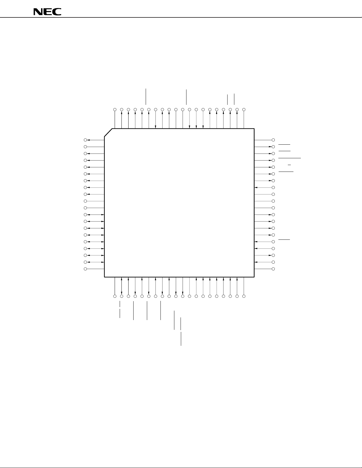
• 80-pin Plastic TQFP (Fine pitch) (12 × 12 mm)
µ
PD70216HGK-10-9EU
µ
PD70216HGK-12-9EU
µ
PD70216HGK-16-9EU
µ
PD70216HGK-20-9EU
NC
A16/PS0
A17/PS1
A18/PS2
A19/PS3
REFRQ
HLDRQ
HLDAK
80 79 78 77 76 75 74 73 72 71 70 69 68 67 66 65 64 63 62 61
AD15
NC
AD14
AD13
AD12
AD11
AD10
AD9
AD8
GND
GND
AD7
AD6
AD5
AD4
AD3
AD2
AD1
AD0
NC
1
2
3
4
5
6
7
8
9
10
11
12
13
14
15
16
17
18
19
20
21 22 23 24 25 26 27 28 29 30 31 32 33 34 35 36 37 38 39 40
RESOUT
VDDVDDRESET
READY
NMI
BS2
BS1
BS0
MRD
µ
PD70208H, 70216H
IORD
NC
60
59
58
57
56
55
54
53
52
51
50
49
48
47
46
45
44
43
42
41
NC
MWR
IOWR
BUSLOCK
BUFR/W
BUFEN
CLKOUT
X1
X2
GND
GND
UBE
ASTB
QS0
QS1
POLL
TCTL2
TOUT2
TCLK
NC
NC
END/TC
DMARQ0
D
D
X
X
DMAAK1
DMARQ1
DMAAK0
DMAAK2
DMARQ2
DMAAK3/T
DMARQ3/R
Data Sheet U13225EJ4V0DS00
DD
V
INTP1
INTP2
INTP3
INTP4
INTP5
INTAK/SRDY/TOUT1
INTP6
INTP7
NC
7

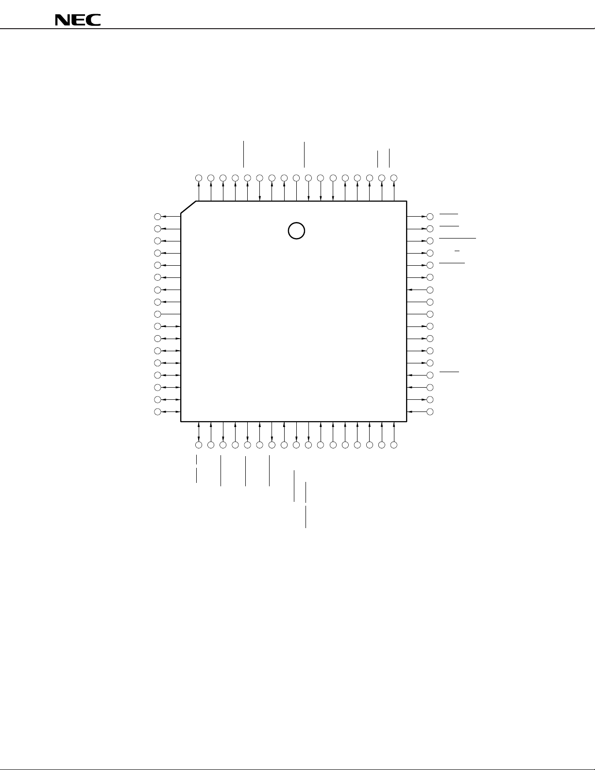
• 68-pin Plastic QFJ (950 × 950 mil)
µ
PD70216HLP-10
µ
PD70216HLP-12
µ
PD70216HLP-16
µ
PD70216HLP-20
A16/PS0
A17/PS1
A18/PS2
A19/PS3
REFRQ
HLDRQ
HLDAK
RESOUT
VDDRESET
READY
NMI
BS2
BS1
BS0
µ
PD70208H, 70216H
MRD
IORD
AD15
AD14
AD13
AD12
AD11
AD10
AD9
AD8
GND
AD7
AD6
AD5
AD4
AD3
AD2
AD1
AD0
9 8 7 6 5 4 3 2 1 68 67 66 65 64 63 62 61
10
11
12
13
14
15
16
17
18
19
20
21
22
23
24
25
26
27
28 29 30 31 32 33 34 35 36 37 38 39 40 41 42 43
D
D
X
X
INTP1
INTP2
END/TC
DMARQ0
DMAAK1
DMARQ1
DMAAK0
DMAAK2
DMARQ2
DMARQ3/R
DMAAK3/T
INTP3
INTP4
INTP5
60
59
58
57
56
55
54
53
52
51
50
49
48
47
46
45
44
INTP6
INTP7
MWR
IOWR
BUSLOCK
BUFR/W
BUFEN
CLKOUT
X1
X2
GND
UBE
ASTB
QS0
QS1
POLL
TCTL2
TOUT2
TCLK
INTAK/SRDY/TOUT1
8
Data Sheet U13225EJ4V0DS00
PIN NAMES
A8-A15 : Address Bus
A16/PS0-A19/PS3 : Address/Processor Status
AD0-AD15 : Address Bus/Data Bus
ASTB : Address Strobe
BS0-BS2 : Bus Status
BUFEN : Buffer Enable
BUFR/W : Buffer Read/Write
BUSLOCK : Bus Lock
CLKOUT : Clock Output
DMAAK0-DMAAK2 : DMA Acknowledge
DMAAK3/TXD : DMA Acknowledge/Transmit Data
DMARQ0-DMARQ2 : DMA Request
DMARQ3/RXD : DMA Request/Receive Data
END/TC : End/Terminal Count
GND : Ground
High : High Level Output
HLDAK : Hold Acknowledge
HLDRQ : Hold Request
IC : Internally Connected
INTAK/SRDY/TOUT1 : Interrupt Acknowledge/Serial Ready/Timer Output 1
INTP1-INTP7 : Interrupt Request from Peripherals
IORD : I/O Read
IOWR : I/O Write
MRD : Memory Read
MWR : Memory Write
NC : No Connection
NMI : Non-Maskable Interrupt Request
POLL : Poll
QS0, QS1 : Queue Status
READY : Ready
REFRQ : Refresh Request
RESET : Reset
RESOUT : Reset Output
TCLK : Timer Clock
TCTL2 : Timer Control 2
TOUT2 : Timer Output 2
UBE : Upper Byte Enable
DD : Power Supply
V
X1, X2 : Crystal
µ
PD70208H, 70216H
Data Sheet U13225EJ4V0DS00
9
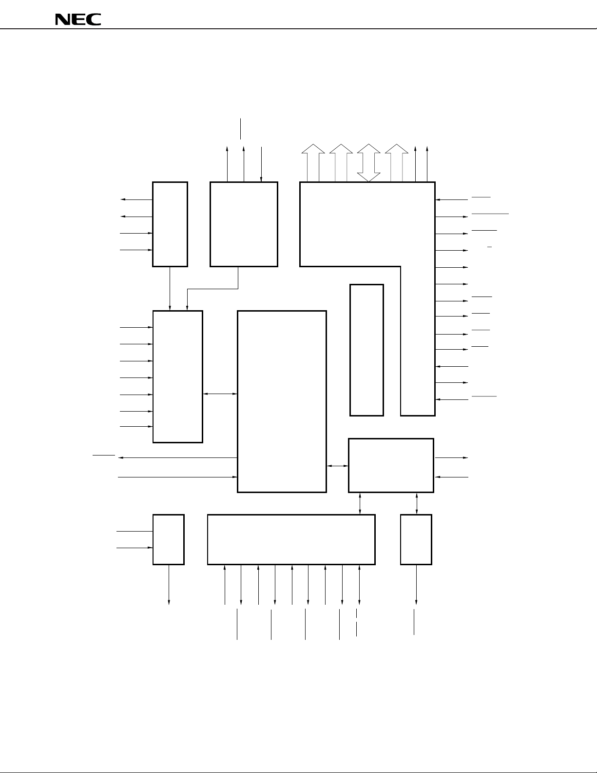
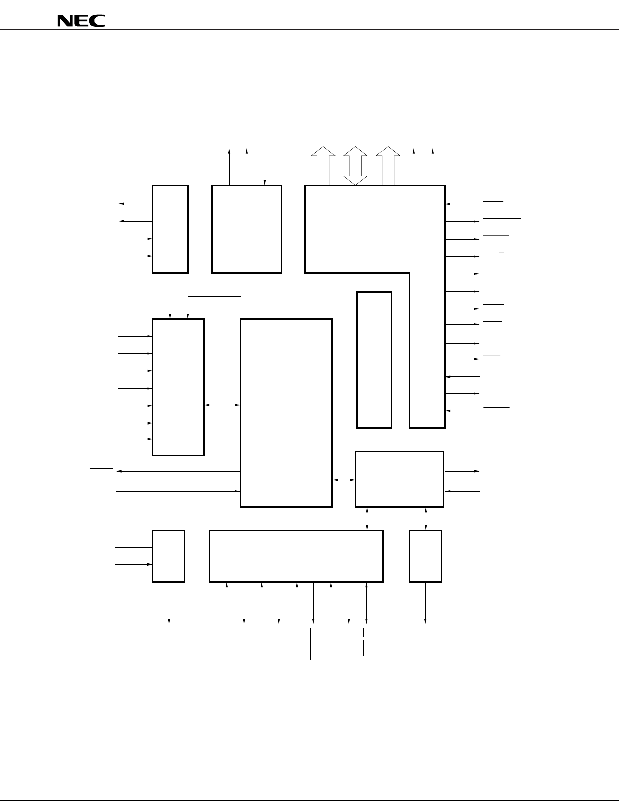
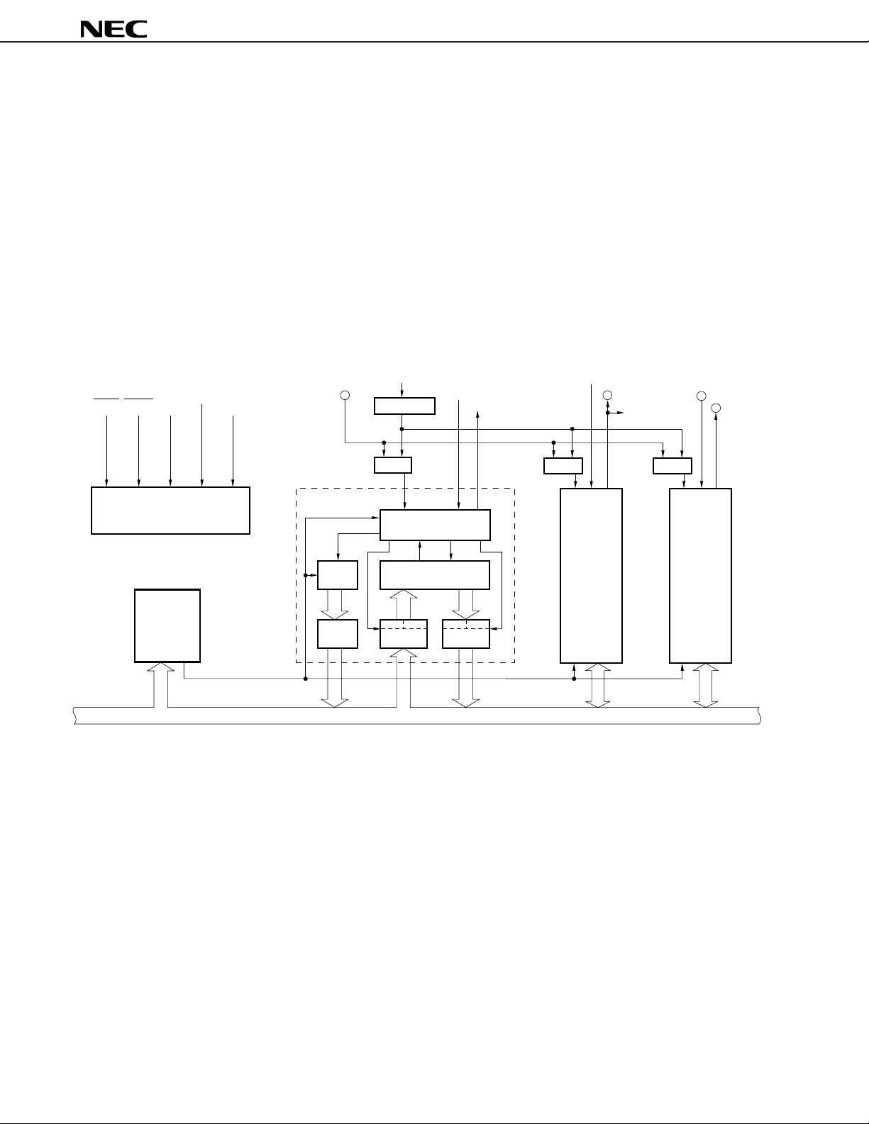
BLOCK DIAGRAM
(1) V40HL
µ
PD70208H, 70216H
TOUT2
TOUT1
TCTL2
TCLK
INTP7
INTP6
INTP5
INTP4
INTP3
INTP2
TCU
ICU
XD
T
SCU
SRDY
XD
R
CPU
A16/PS0-A19/PS3
A8-A15
WCU
AD0-AD7
BIU
QS1
BS0-BS2
QS0
POLL
BUSLOCK
BUFEN
BUFR/W
High
ASTB
IOWR
IORD
MWR
MRD
READY
RESOUT
RESET
INTP1
INTAK
NMI
X2
X1
CG
CLKOUT
DMAAK0
DMARQ0
DMAU
DMAAK1
DMARQ1
DMAAK2
DMARQ2
DMARQ3
CPU : Central Processing Unit REFU : Reflesh Control Unit
CG : Clock Generator TCU : Timer/Count Unit
BIU : Bus Interface Unit SCU : Serial Control Unit
BAU : Bus Arbitration Unit ICU : Interrupt Control Unit
WCU : Wait Control Unit DMAU : DMA Control Unit
10
Data Sheet U13225EJ4V0DS00
END/TC
DMAAK3
BAU
HLDAK
HLDRQ
REFU
REFRQ
(2) V50HL
µ
PD70208H, 70216H
TOUT2
TOUT1
TCTL2
TCLK
INTP7
INTP6
INTP5
INTP4
INTP3
INTP2
TCU
ICU
XD
T
SCU
SRDY
RXD
CPU
A16/PS0-A19/PS3
AD0-AD15
BIU
WCU
BS0-BS2
QS1
QS0
POLL
BUSLOCK
BUFEN
BUFR/W
UBE
ASTB
IOWR
IORD
MWR
MRD
READY
RESOUT
RESET
INTP1
INTAK
NMI
X2
X1
CG DMAU
CLKOUT
DMAAK0
DMARQ0
DMAAK1
DMARQ1
DMARQ2
DMAAK2
DMARQ3
END/TC
DMAAK3
BAU
HLDAK
HLDRQ
REFU
REFRQ
Data Sheet U13225EJ4V0DS00
11
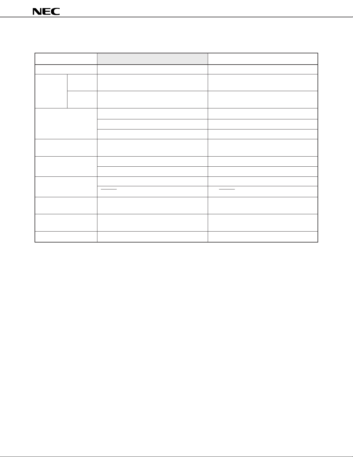
DIFFERENCES FROM V40 AND V50
Item V40, V50V40HL, V50HL
µ
PD70208H, 70216H
Operating supply voltage
Operating
frequency
Clock generator
(CG)
Internal I/O relocation
function
Wait control unit (WCU)
Refresh control unit
(REFU)
Serial control unit (SCU)
DMA control unit (DMAU)
Standby functions
VDD = 5 V
VDD = 3 V
3 V, 5 V
MAX. : 10, 12.5, 16, 20 MHz
MIN. : DC
MAX. : 5, 6.25, 8, 10 MHz
MIN. : DC
Variable scaling factor
Variable instruction cycle time
Maximum input frequency: 40 MHz
Switchable 8-bit boundary or 16-bit boundary
relocation function
Memory space: 5 divisions
I/O space: 3 divisions
Refresh address: 16 bits
REFRQ extended timing supported
Dedicated baud rate generator incorporated
µ
PD71071/71037 subset (either function
selectable)
HALT mode, STOP mode
Note 1
Note 2
5 V
MAX. : 8, 10 MHz
MIN. : 2 MHz
No operation
Fixed scaling factor
Fixed instruction cycle time
Maximum input frequency: 20 MHz
V40: Relocation possible on 8-bit boundary
V50: Relocation possible on 16-bit boundary
Memory space: 3 divisions
I/O space: Not divided
Refresh address: 9 bits
No REFRQ extended timing
No dedicated baund rate generator
incorporated
µ
PD71071 subset
HALT mode only
Notes 1. Divided into 3 when a reset is performed.
2. Not divided when a reset is performed.
12
Data Sheet U13225EJ4V0DS00

µ
PD70208H, 70216H
CONTENTS
1. PIN FUNCTIONS ................................................................................................................................... 15
1.1 LIST OF PIN FUNCTIONS........................................................................................................................... 15
1.2 PROCESSING OF UNUSED PINS.............................................................................................................. 17
2. MEMORY AND I/O CONFIGURATION ................................................................................................ 19
2.1 MEMORY SPACE......................................................................................................................................... 19
2.2 I/O SPACE .................................................................................................................................................... 21
3. CPU ........................................................................................................................................................ 22
4. CG (CLOCK GENERATOR) ................................................................................................................. 24
5. BIU (BUS INTERFACE UNIT) .............................................................................................................. 24
6. BAU (BUS ARBITRATION UNIT) ........................................................................................................ 25
7. WCU (WAIT CONTROL UNIT) ................................................................................................................ 27
7.1 FEATURES ................................................................................................................................................... 27
7.2 RELATION BETWEEN WCU AND READY PIN ........................................................................................ 28
8. REFU (REFRESH CONTROL UNIT).................................................................................................... 29
8.1 FEATURES ................................................................................................................................................... 29
8.2 REFRESH OPERATIONS ............................................................................................................................ 29
9. TCU (TIMER/COUNTER UNIT) ............................................................................................................ 30
9.1 FEATURES ................................................................................................................................................... 30
9.2 TCU INTERNAL BLOCK DIAGRAM........................................................................................................... 30
10. SCU (SERIAL CONTROL UNIT) .......................................................................................................... 31
10.1 FEATURES ................................................................................................................................................... 31
10.2 SCU INTERNAL BLOCK DIAGRAM ........................................................................................................... 31
11. ICU (INTERRUPT CONTROL UNIT) .................................................................................................... 32
11.1 FEATURES ................................................................................................................................................... 32
11.2 ICU INTERNAL BLOCK DIAGRAM ............................................................................................................ 32
12. DMAU (DMA CONTROL UNIT) ............................................................................................................ 33
12.1 FEATURES ................................................................................................................................................... 33
12.2 DMAU INTERNAL BLOCK DIAGRAM ....................................................................................................... 33
13. STANDBY FUNCTIONS........................................................................................................................ 34
14. RESET OPERATION ............................................................................................................................. 3 4
15. INSTRUCTION SET............................................................................................................................... 35
Data Sheet U13225EJ4V0DS00
13

µ
PD70208H, 70216H
16. ELECTRICAL SPECIFICATIONS......................................................................................................... 66
16.1 AT 5 V OPERATION .................................................................................................................................... 66
16.2 AT 3 V OPERATION .................................................................................................................................... 75
17. PACKAGE DRAWINGS ........................................................................................................................ 100
18. RECOMMENDED SOLDERING CONDITIONS ................................................................................... 103
14
Data Sheet U13225EJ4V0DS00
µ
PD70208H, 70216H
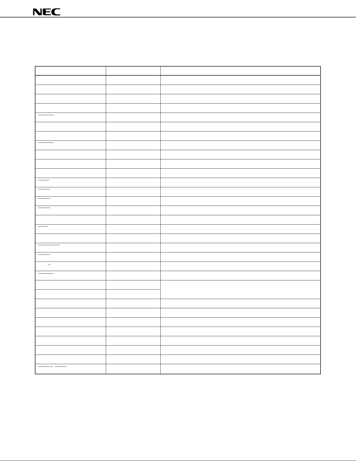
1. PIN FUNCTIONS
1.1 LIST OF PIN FUNCTIONS
Pin Name Input/Output Function
Note 3
Note 3
Note 3
Note 3
Note 3
Note 2, 3
Note 2, 3
Note 3
Note 3
Note 3
Note 1, 3
Note 3
3-state I/O Time-division address/data bus
3-state I/O Time-division address/data bus
3-state output Address bus
3-state output Time-division address/processor status
3-state output Memory read strobe
3-state output Memory read strobe
3-state output I/O read strobe
3-state output I/O write strobe
3-state output Data bus upper byte enable
3-state output High level output
3-state output Bus lock
3-state output Buffer read/write
3-state output Buffer enable
3-state output Bus status
AD0 to AD15
AD0 to AD7
A8 to A15
A16/PS0 to A19/PS3
REFRQ Output Refresh request
HLDRQ Input Bus hold request
HLDAK Output Bus hold acknowledge
RESET Input Reset
RESOUT Output System reset output
READY Input Bus cycle end
NMI Input Non-maskable interrupt
MRD
MWR
IORD
IOWR
ASTB Output Address strobe
Note 1, 3
UBE
Note 2
High
BUSLOCK
POLL Input Floating-point operation processor polling
BUFR/W
BUFEN
X1 Input Crystal/external clock
X2 —
CLKOUT Output Clock output
BS0 to BS2
QS0, QS1 Output Queue status
TOUT2 Output Timer 2 output
TCTL2 Input Timer 2 control
TCLK Input Timer clock
INTP1 to INTP7 Input Maskable interrupts
INTAK/SRDY/TOUT1 Output Interrupt acknowledge/serial reception ready/timer 1 output
Notes 1. V50HL only
2. V40HL only
3. These pins are provided with a latch. Therefore, when they go into a high-impedance state, they hold
the status before the high-impedance state until driven by an external device. It is not necessary to pull
up or down the data bus. To invert the level of the pin that goes into a high-impedance state by an
external device, a drive current higher than the latch invert current (I
Data Sheet U13225EJ4V0DS00
ILH, IILL) is necessary.
15
µ
PD70208H, 70216H
Pin Name Input/Output Function
DMAAK3/TXD Output DMA acknowledge 3/serial transmit data
DMARQ3/RXD Input DMA request 3/serial receive data
DMAAK0 to DMAAK2 Output DMA acknowledge
DMARQ0 to DMARQ2 Input DMA request
END/TC I/O DMA service forcible termination/DMA service completion
VDD — Positive power supply pin
GND — Ground potential pin
IC — Internal connection pin (External connection impossible)
16
Data Sheet U13225EJ4V0DS00
µ
PD70208H, 70216H
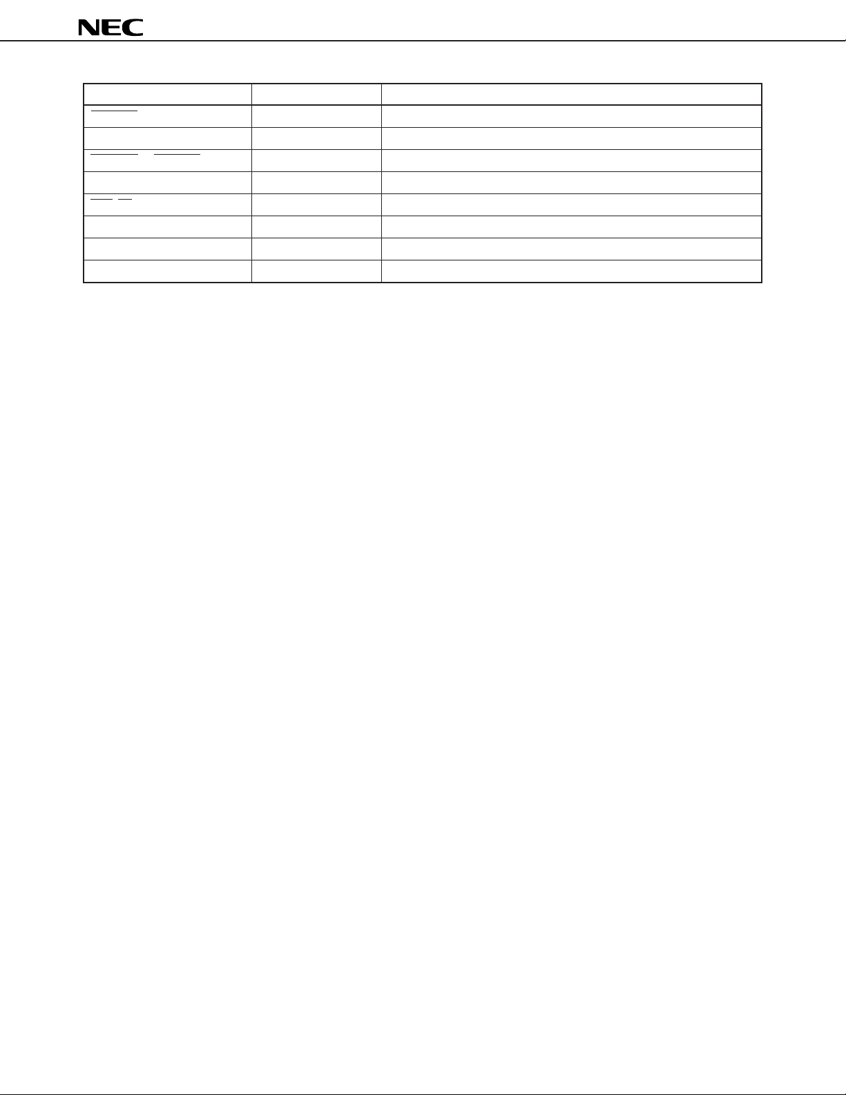
1.2 PROCESSING OF UNUSED PINS
Table 1-1 shows the processing (recommended connection) of the unused pins. Use of a resistor with a resistance of
1 to 10 kΩ is recommended to connect these pins to VDD or GND via resistor.
Table 1-1. Processing of Unused Pins
Pin Name Input/Output Recommended Connection
AD0 to AD15
AD0 to AD7
A8 to A15
A16/PS0 to A19/PS3 3-state output
REFRQ Output
HLDRQ Input Connect to GND via resistor
HLDAK Output Open
RESOUT Output Open
READY Input Connect to VDD via resistor
NMI Input Connect to GND via resistor
MRD 3-state output Open
MWR 3-state output
IORD 3-state output
IOWR 3-state output
ASTB Output
Note 1
UBE
Note 2
High
BUSLOCK 3-state output
POLL Input Connect to GND via resistor
BUFR/W 3-state output Open
BUFEN 3-state output
CLKOUT Output Open
BS0 to BS2 3-state output
QS0, QS1 Output
TOUT2 Output
TCTL2 Input Connect to GND via resistor
TCLK Input
INTP1 to INTP7 Input Open
INTAK/SRDY/TOUT1 Output
DMAAK3/TxD Output
DMARQ3/RxD Input Connect to GND via resistor
DMAAK0 to DMAAK2 Output Open
DMARQ0 to DMARQ2 Input Connect to GND via resistor
END/TC I/O Individually connect to VDD via resistor
Note 1
Note 2
Note 2
3-state I/O Open
3-state I/O
3-state output
3-state output
Output
Notes 1. V50HL only
2. V40HL only
Data Sheet U13225EJ4V0DS00
17
µ
PD70208H, 70216H
Remark The circuit configuration of the latch is as illustrated below. To invert the level of the pin with a latch, a drive
current higher than the latch invert current is necessary.
(1) Output pin
(2) I/O pin
Hi-Z
control
Hi-Z
control
Output buffer
Output buffer
Input buffer
Latch
Output pin
address bus,
control bus
Latch
I/O pin
(data bus)
18
Data Sheet U13225EJ4V0DS00
2. MEMORY AND I/O CONFIGURATION
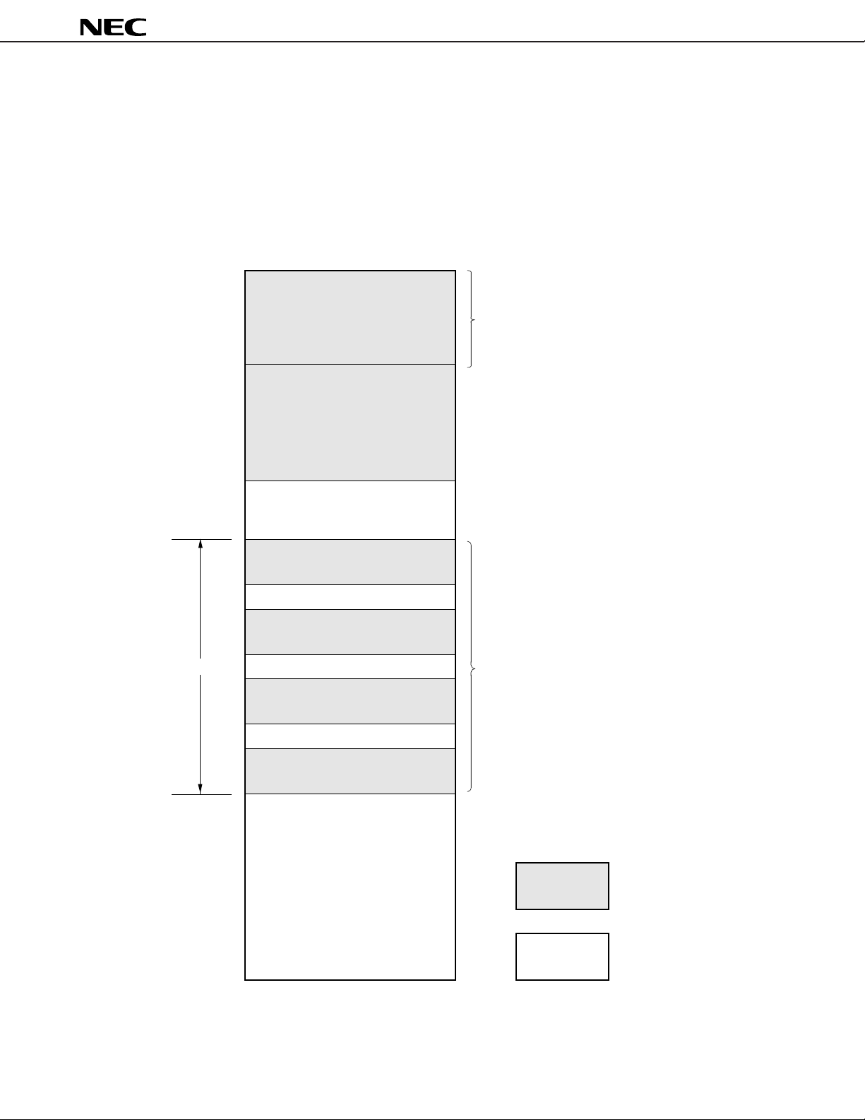
2.1 MEMORY SPACE
The V40HL and V50HL can access a 1M-byte (512K-word) memory space.
Figure 2-1. Memory Map
FFFFFH
Reserved
FFFFCH
FFFFBH
Dedicated
FFFF0H
FFFEFH
General Use
µ
PD70208H, 70216H
A0-A19
00400H
003FFH
Interrupt Vector Table
00000H
Figure 2-2. Interface with Memory (1/2)
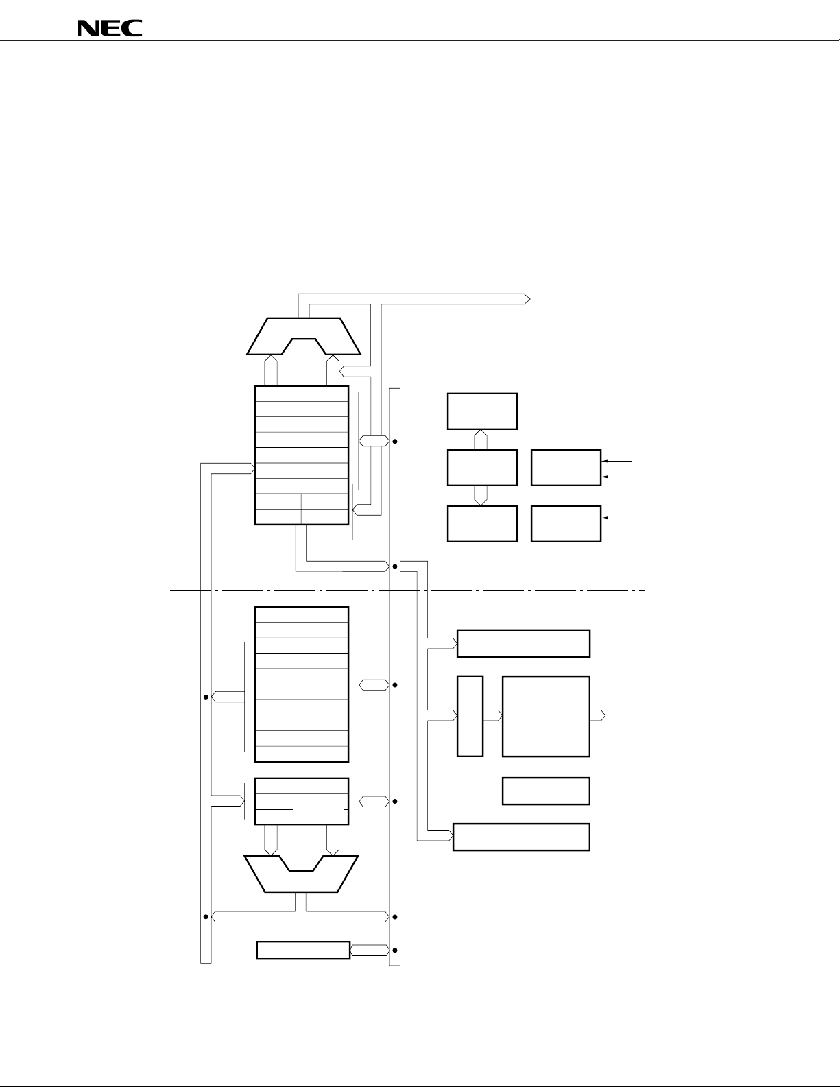
(a) V40HL
Address Bus (20)
Memory
1M Byte
8
D0-D7
Data Bus (8)
Data Sheet U13225EJ4V0DS00
19
Figure 2-2. Interface with Memory (2/2)
(b) V50HL
µ
PD70208H, 70216H
A1-A19
A0
UBE
D0-D15
Address Bus (19)
19 19
BSEL BSEL
Memory
Upper Bank
512K Byte
D8-D15 D0-D7
8
Data Bus (16)
Memory
Lower Bank
512K Byte
8
20
Data Sheet U13225EJ4V0DS00
µ
PD70208H, 70216H
2.2 I/O SPACE
In the V40HL and V50HL, I/Os up to 64K bytes (32K words) can be accessed in an area independent of the memory.
The various on-chip peripheral LSIs are set by accessing the system I/O area.
Extended functions added to those of the V40 and V50 are mapped onto unused V40 and V50 registers and the reserved
area.
The I/O map is shown in Figure 2-3.
Figure 2-3. I/O Map
FFFFH
Area used for setting of I/O boundary,
System I/O Area
FFE0H
FFDFH
Reserved Area
WCU, REFU, baud rate generator, etc.,
and DMAU, ICU, TCU and SCU allocation.
FF00H
FEFFH
256 Bytes
DMAU
ICU
The DMAU, ICU, TCU and SCU
are allocated within any 256 bytes.
TCU
SCU
Internal I/O Area
0000H
Data Sheet U13225EJ4V0DS00
External I/O Area
21
µ
PD70208H, 70216H
3. CPU
The CPU has the same functions as the V20HLTM and V30HLTM. In hardware terms, there are some changes regarding
the use of the bus with on-chip peripherals, but in software terms the CPU is fully compatible.
The internal block diagram of the CPU is shown in Figure 3-1.
Figure 3-1. Internal Block Diagram of CPU (1/2)
(a) V40HL
Internal Address/Data Bus (20)
To BIU
ADM
TC
TA
TB
Q0
Q2
PS
SS
DS0
DS1
PFP
DP
TEMP
LC
PC
AW
BW
CW
DW
IX
IY
BP
SP
SHIFTER
Q1
Q3
T-STATE
CONTROL
CYCLE
DECISION
QUEUE
CONTROL
EFFECTIVE ADDRESS
GENERATOR
ADDRESS
REGISTER
µ
Queue Data Bus (8)
INSTRUCTION DECODER
INTERRUPT
CONTROL
STANDBY
CONTROL
INSTRUCTION
µ
ROM
SEQUENCE
µ
CONTROL
BCU
EXU
29
Micro Data Bus
NMI
INT
(From ICU)
CLOCK
(From CG)
22
Sub Data Bus
(16)
ALU
PSW
Main Data Bus
(16)
Data Sheet U13225EJ4V0DS00
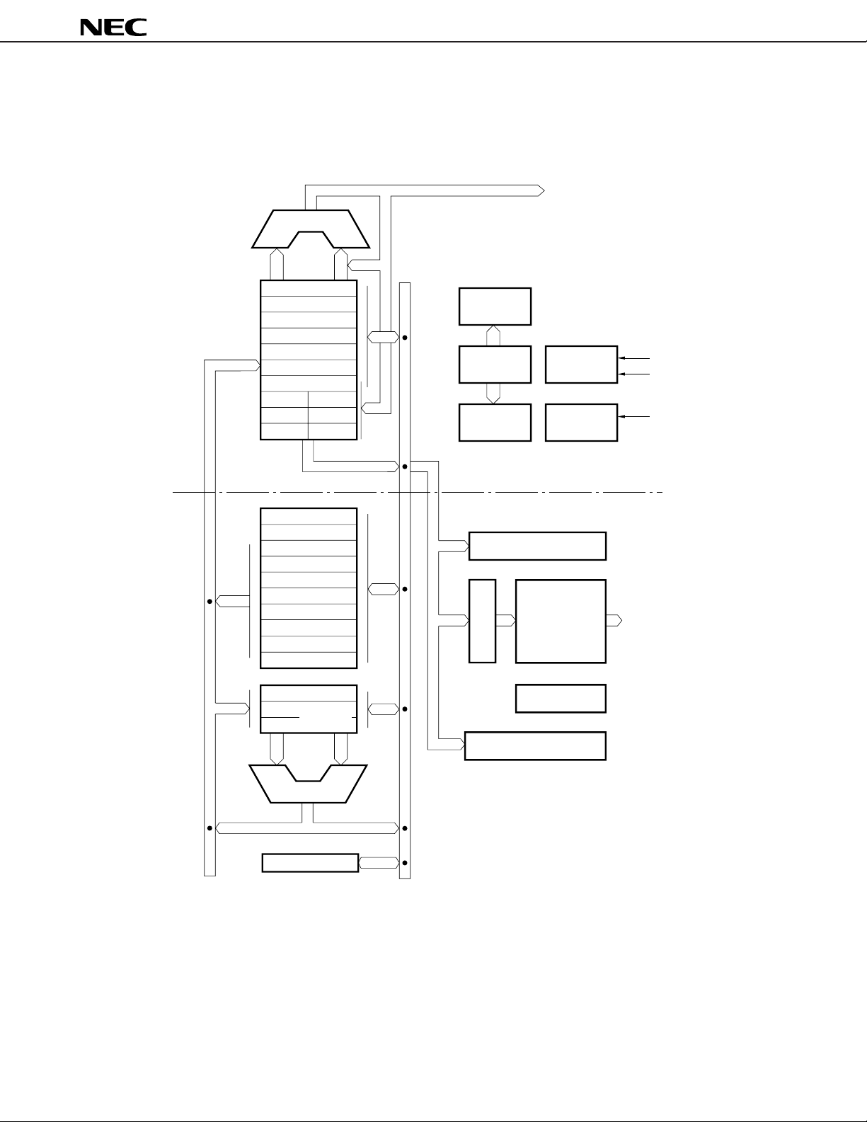
Figure 3-1. Internal Block Diagram of CPU (2/2)
(b) V50HL
Internal Address/Data Bus (20)
To BIU
ADM
µ
PD70208H, 70216H
PS
SS
DS0
DS1
PFP
DP
TEMP
Q0
Q2
Q4 Q5
LC
PC
AW
BW
CW
DW
IX
IY
BP
SP
TC
TA
SHIFTER
TB
Q1
Q3
T-STATE
CONTROL
CYCLE
DECISION
QUEUE
CONTROL
EFFECTIVE ADDRESS
GENERATOR
ADDRESS
REGISTER
µ
Queue Data Bus (8)
INSTRUCTION DECODER
INTERRUPT
CONTROL
STANDBY
CONTROL
INSTRUCTION
µ
ROM
SEQUENCE
µ
CONTROL
BCU
EXU
29
Micro Data Bus
NMI
INT
(From ICU)
CLOCK
(From CG)
Sub Data Bus
(16)
ALU
PSW
Main Data Bus
(16)
Data Sheet U13225EJ4V0DS00
23
µ
PD70208H, 70216H
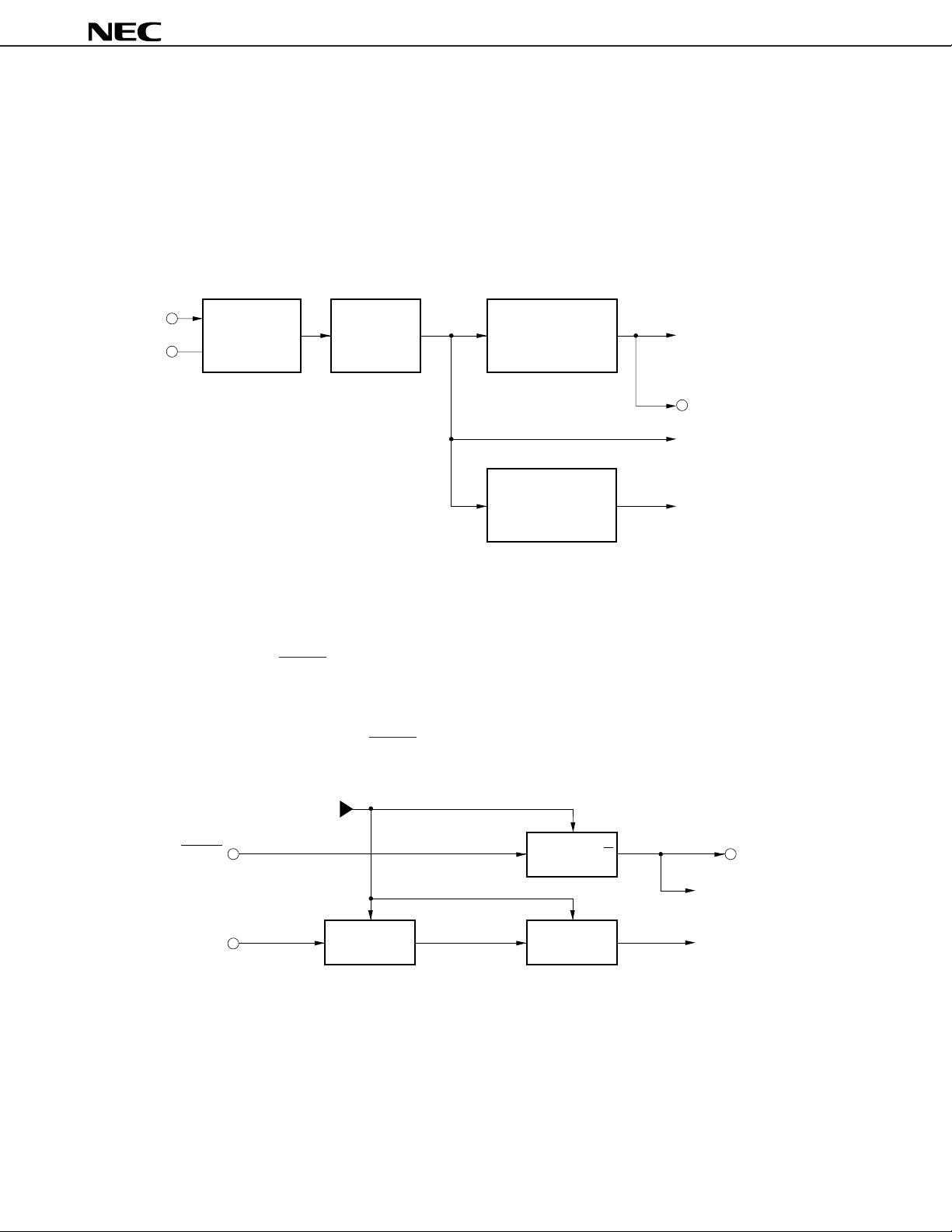
4. CG (CLOCK GENERATOR)
The CG generates a clock at a frequency of 1/2, 1/4, 1/8 or 1/16 that of the crystal and oscillator connected to the X1
and X2 pins, supplies it as the CPU operating clock and outputs it externally as the CLKOUT pin output.
The interrupt cycle time can be changed according to the oscillator scaling factor. The scaling factor can be set by a
system I/O area register.
Figure 4-1. Internal Block Diagram of CG
X1
X2
Oscillator
f
XX
Divide-by-2
Scaler
Divide-by-1-to-8
Scaler
Divide-by-2-to-16
Scaler
f
X
CPU, DMAU, REFU, SCU
CLKOUT
Baud Rate Counter (BRC)
TCU
5. BIU (BUS INTERFACE UNIT)
The BIU controls the data bus, address bus and control bus pins. These buses are used by the CPU, DMAU (DMA control
unit) and REFU (refresh control unit).
The BIU synchronizes the RESET input signal and READY input signal using the CLOCK signal generated by the clock
generator (CG). In addition to being supplied to the inside of the V40HL and V50HL, the synchronized reset signal is also
output externally from the RESOUT pin. The synchronized READY signal is supplied to the internal CPU, DMAU and REFU.
Figure 5-1. RESET and READY Signal Synchronization
24
RESET
READY
CLOCK
CK ↑
QD
Data Sheet U13225EJ4V0DS00
CK ↓
CK ↓
QD
QD
RESOUT
To Internal Units
To Internal Units
6. BAU (BUS ARBITRATION UNIT)
The BAU performs bus arbitration among bus masters.
A list of bus masters (units which can acquire the bus) is shown below.
Table 6-1. Bus Masters
Bus Master Bus Cycle
µ
PD70208H, 70216H
CPU
DMAU
REFU
External bus master
(HLDRQ pin input)
The relative priorities of the bus masters are shown below.
High CPU (when BUSLOCK prefix is used)
REFU (highest priority: when given number of requests are reached)
DMAU
HLDRQ pin
CPU (normal CPU cycle)
Low REFU (lowest priority: cycle steal)
BAU bus arbitration is performed as follows.
A bus master such as the CPU, DMAU, REFU, etc., incorporated in the V40HL and V50HL normally release the bus at
the end of the bus cycle currently being executed, as shown in Figure 6-1. However, in the case of a bus master connected
to the HLDRQ pin, or cascaded external DMA controllers, for instance, the situation is as shown in Figure 6-2. The V40HL
and V50HL request return of the bus by inactivating the acknowledge signal (HLDAK), and on receiving this request, the
external bus master holding the bus should release the bus by dropping the bus hold request signal (HLDRQ). The V40HL
and V50HL-internal bus master with the highest priority is kept waiting until the bus hold request signal is dropped. This
is called a bus wait operation.
Program fetch, data read/write
DMA cycle
Refresh cycle
Bus cycle driven by external device
Data Sheet U13225EJ4V0DS00
25
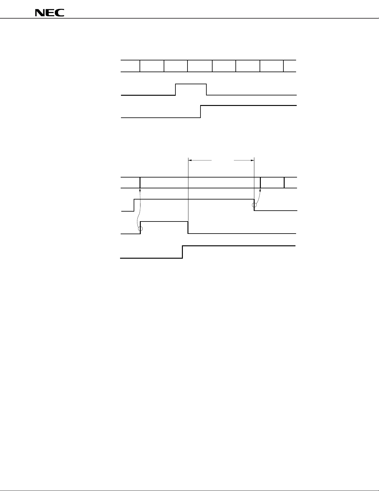
Figure 6-1. Internal Bus Cycles
µ
PD70208H, 70216H
Bus Cycle
Internal DMA Request
Internal Refresh Request
(Highest Priority)
Bus Cycle
HLDRQ Pin
HLDAK Pin
CPU CPU DMA Refresh Refresh Refresh
Figure 6-2. Bus Wait Operation
Bus Wait
Bus Release Refresh
Note
Internal Refresh Request
(Highest Priority)
Note The period in which the external bus master which has been given the bus after its release by the V40HL and
V50HL can use the bus.
26
Data Sheet U13225EJ4V0DS00
µ
PD70208H, 70216H
7. WCU (WAIT CONTROL UNIT)
The WCU has the function of automatically inserting a wait state (TW) of 0 to 3 clock cycles in a CPU, DMAU or REFU
bus cycle.
7.1 FEATURES
Automatic setting of 0 to 3 waits for a CPU memory bus cycle
•
1M-byte memory space can be divided into 5
•
64K-byte I/O space can be divided into 3
•
Automatic setting of 0 to 3 waits for an external I/O cycle
•
Automatic setting of 0 to 3 waits for a DMA cycle
•
Automatic setting of 0 to 3 waits for a refresh cycle
•
Same as V40 and V50 directly after a reset (memory space divided into 3, no division of I/O space)
•
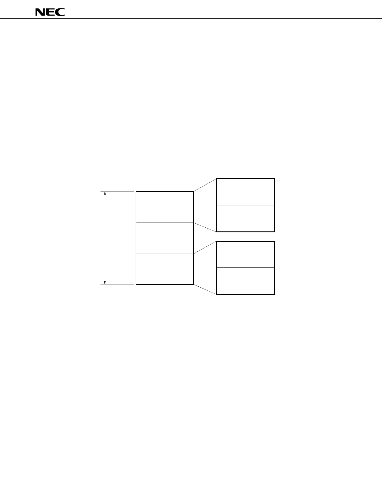
Figure 7-1. Example of Memory Space Division
Upper Sub
FFFFFH
Memory Block
Upper Memory Block
1 M-Byte
Memory Area
00000H
Remark The division specification and the size of each block are set by means of a system I/O area register.
Middle Memory Block
Lower Memory Block
Lower Sub
Memory Block
Data Sheet U13225EJ4V0DS00
27
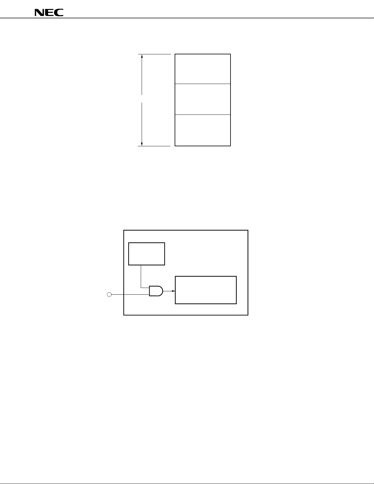
Figure 7-2. Example of I/O Space Division
FFFFH
Upper I/O Block
µ
PD70208H, 70216H
64K-Byte I/O Area
0000H
Remark The division specification and the size of each block are set by means of a system I/O area register.
7.2 RELATION BETWEEN WCU AND READY PIN
When wait cycles exceeding 3 clock cycles are necessary, the WCU and the READY signal pin can be used in
combination. The number of wait cycles specified by the WCU set value or the number of wait cycles under READY control,
whichever is larger, is inserted.
Figure 7-3. WCU and READY Control
WCU
Middle I/O Block
Lower I/O Block
V40HL/V50HL
28
READY
Bus Control
Data Sheet U13225EJ4V0DS00

µ
PD70208H, 70216H
8. REFU (REFRESH CONTROL UNIT)
The REFU generates refresh cycles required for refreshing of external DRAM. Refresh enabling/disabling and the refresh
interval can be set programmably.
8.1 FEATURES
Lowest-priority refreshing/highest-priority refreshing
•
7-refresh queue
•
16-bit refresh address
•
REFRQ extended timing supported (REFRQ active from T1 state)
•
8.2 REFRESH OPERATIONS
The REFU has two priorities. Normally, it has the lowest priority, and a refresh cycle cannot be started unless the bus
is completely idle. However, if there are 7 or more pending refresh requests, it is given the highest priority, and it requests
the bus master holding the bus to relinquish it. (See 6. BAU.)
The refresh address is output on A0 to A15. Every refresh cycle the refresh address is incremented by 1 (for the V40HL)
or by 2 (for the V50HL), and the next refresh address is generated.
In a refresh cycle, a low-level signal is output on the low address pins (A16 to A19).
This refresh address is not affected by a reset. When the device is powered on, the refresh address is undefined.
Data Sheet U13225EJ4V0DS00
29
µ
PD70208H, 70216H
9. TCU (TIMER/COUNTER UNIT)
The TCU incorporates 3 counters, and can be used as a timer, event counter, rate generator, etc. Functionally it is a
subset of the
9.1 FEATURES
3 × 16-bit counters
•
Six programmable count modes
•
Binary/BCD count
•
Multiple latch command
•
Choice of two input clocks: internal/external
•
9.2 TCU INTERNAL BLOCK DIAGRAM
µ
PD71054.
IORDIOWR
Read/Write Control
Register)
Note 1
TMD
(Mode
Note 2
TCU
Selection
Signal
TCLK
(External)
TCT #0
Status
Register
(8)
Status
Latch
(8) (8) (8)
CLOCK
Prescaler
Down Counter (16)
H(8) L(8)
Count
Register
Internal Data Bus
Notes 1. A0 or A1 (Set by a system I/O area register)
2. A1 or A2 (Set by a system I/O area register)
Control Logic
(16)
H(8) L(8)
TCTL0=High
TOUT0 (To INTL0)
(16)
Count
Latch
TCTL1=High
TOUT1
(External
)
TCTL2
To INTL2/SCU
SWSWSW
TCT #1 TCT #2
(External)
TOUT2
(External)
30
Data Sheet U13225EJ4V0DS00
 Loading...