


Motorola MC74LVX4245DW, MC74LVX4245DT Datasheet
SEMICONDUCTOR TECHNICAL DATA
"
!
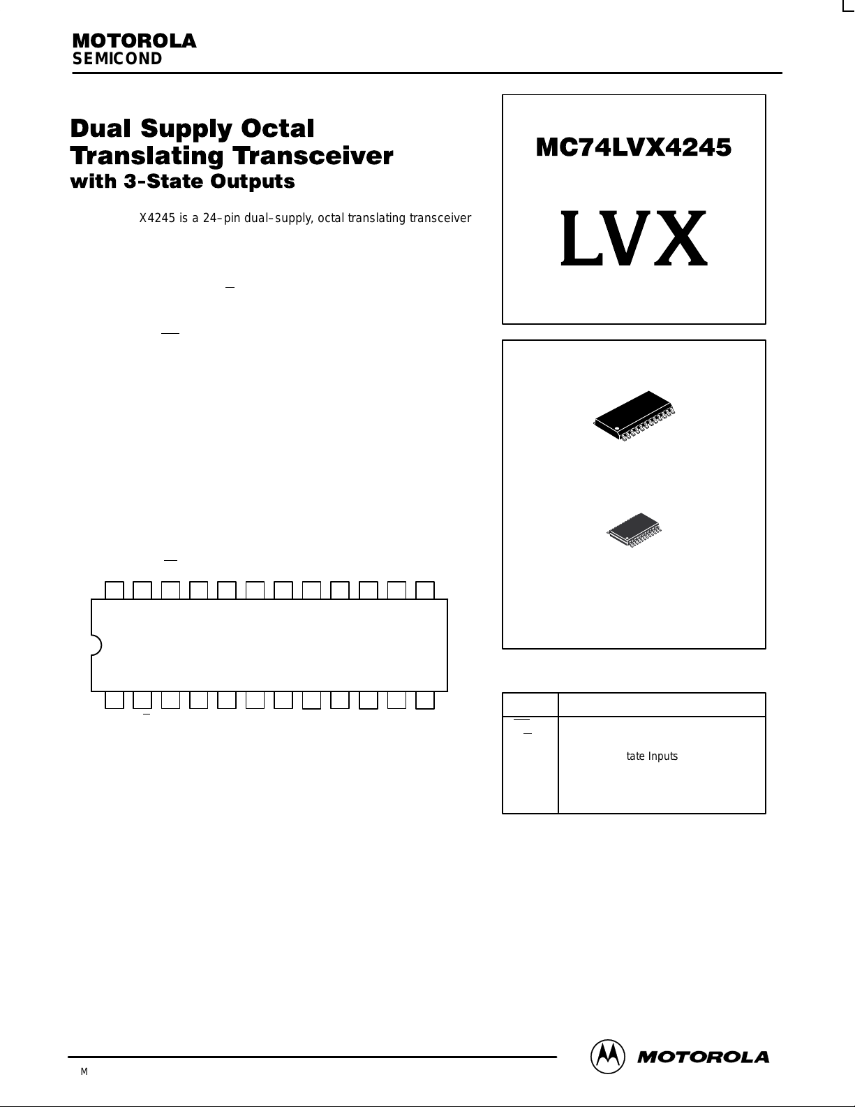
The 74LVX4245 is a 24–pin dual–supply, octal translating transceiver
that is designed to interface between a 5V bus and a 3V bus in a mixed
3V/5V supply environment such as laptop computers using a 3.3V CPU
and 5V LCD display. The A port interfaces with the 5V bus; the B port
interfaces with the 3V bus.
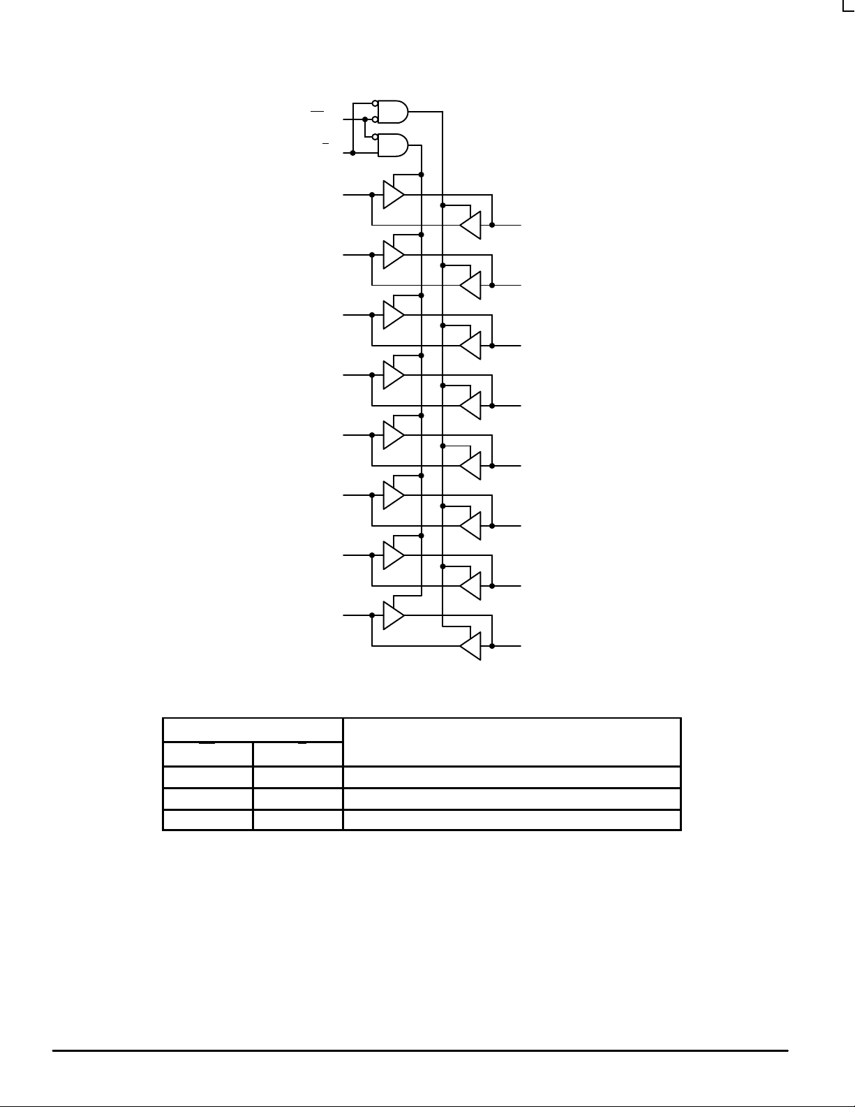
The Transmit/Receive (T/R
Transmit (active–High) enables data from the A port to the B port.
Receive (active–Low) enables data from the B port to the A port. The
Output Enable (OE
placing them in 3–State.
) input, when High, disables both A and B ports by
• Bi–directional Interface Between 5V and 3V Buses
• Control Inputs Compatible with TTL Level
• 5V Data Flow at A Port and 3V Data Flow at B Port
• Outputs Source/Sink 24mA at 5V Bus and 12mA at 3V Bus
• Guaranteed Simultaneous Switching Noise Level and Dynamic
Threshold Performance
• Available in SOIC and TSSOP Packages
• Functionally Compatible with the 74 Series 245
) input determines the direction of data flow.
LVX
LOW–VOLTAGE CMOS
DW SUFFIX
24–LEAD PLASTIC SOIC PACKAGE
CASE 751E–04
V
V
OE
CCB
CCB
2324 22 21 20 19 18
21 34567
V
T/R
CCA
B0 B1 B2 B3 B4 B5 B6
A0 A1 A2 A3 A4 A5 A6 A7
Figure 1. 24–Lead Pinout
(Top View)
17
B7 GND
16
9
8
15
10
14
13
11
12
GND GND
24–LEAD PLASTIC TSSOP PACKAGE
PIN NAMES
Pins
OE
T/R
A0–A7
B0–B7
DT SUFFIX
CASE 948H–01
Function
Output Enable Input
Transmit/Receive Input
Side A 3–State Inputs or 3–State
Outputs
Side B 3–State Inputs or 3–State
Outputs
7/97
Motorola, Inc. 1997
1
REV 2
MC74LVX4245
OPERATING MODE
OE
T/R 2
22
A0
A1
A2
A3
A4
A5
A6
A7
10
3
21
B0
4
20
B1
5
19
B2
6
18
B3
7
17
B4
8
16
B5
9
15
B6
14
B7
Figure 2. Logic Diagram
INPUTS
OE T/R
L L B Data to A Bus
L H A Data to B Bus
H X Z
H = High Voltage Level; L = Low V oltage Level; Z = High Impedance State; X = High or Low Voltage Level
and Transitions are Acceptable; For ICC reasons, Do Not Float Inputs
MOTOROLA LVX Data — Low–Voltage CMOS Logic
2
Non–Inverting
BR1492 — Rev 0
MC74LVX4245
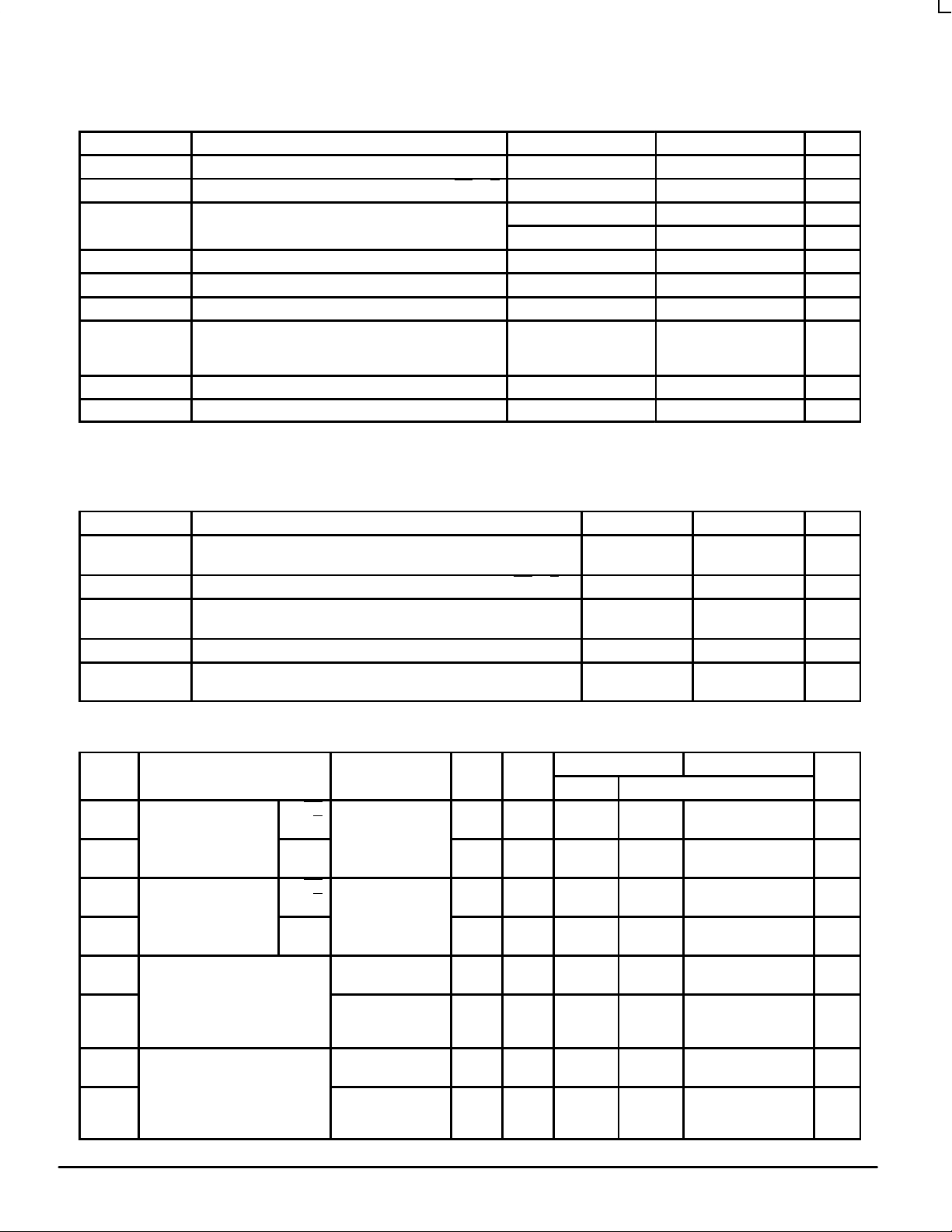
ABSOLUTE MAXIMUM RATINGS*
Symbol Parameter Value Condition Unit
V
, V
CCA
CCB
V
I
V
I/O
I
IK
I
OK
I
O
ICC, I
GND
T
STG
Latchup DC Latchup Source/Sink Current ±300 mA
* Absolute maximum continuous ratings are those values beyond which damage to the device may occur. Exposure to these conditions or conditions
beyond those indicated may adversely affect device reliability. Functional operation under absolute–maximum–rated conditions is not implied.
RECOMMENDED OPERATING CONDITIONS
Symbol Parameter Min Max Unit
V
, V
CCA
CCB
V
I
V
I/O
T
A
∆t/∆V Minimum Input Edge Rate
DC Supply Voltage –0.5 to +7.0 V
DC Input Voltage OE, T/R –0.5 to V
DC Input/Output Voltage An –0.5 to V
Bn –0.5 to V
DC Input Diode Current OE, T/R ±20 VI < GND mA
DC Output Diode Current ±50 VO < GND; VO > V
DC Output Source/Sink Current ±50 mA
DC Supply Current Per Output Pin
Storage Temperature Range –65 to +150 °C
Supply Voltage V
Input Voltage OE, T/R 0 V
Input/Output Voltage An
Operating Free–Air Temperature –40 +85 °C
VIN from 30% to 70% of VCC; VCC at 3.0V , 4.5V, 5.5V
Maximum Current at I
Maximum Current at I
CCA
CCB
V
CCA
CCB
Bn
+0.5 V
CCA
+0.5 V
CCA
+0.5 V
CCB
±50
±200
±100
4.5
2.7
0
0
0 8 ns/V
V
V
5.5
3.6
CCA
CCA
CCB
CC
mA
mA
V
V
V
DC ELECTRICAL CHARACTERISTICS
Symbol Parameter Condition V
V
IHA
V
IHB
V
ILA
V
ILB
V
OHA
V
OHB
V
OLA
V
OLB
LVX Data — Low–Voltage CMOS Logic
BR1492 — Rev 0
Minimum HIGH Level
Input Voltage
Maximum LOW Level
Input Voltage
Minimum HIGH Level
Output Voltage
Maximum LOW Level
Output Voltage
An,OE
T/R
Bn
An,OE
T/R
Bn
V
≤ 0.1V
OUT
or
≥ VCC – 0.1V
V
≤ 0.1V
OUT
or
≥ VCC – 0.1V
I
= –100µA
OUT
IOH = –24mA
I
= –100µA
OUT
IOH = –12mA
IOH = –8mA
I
= 100µA
OUT
IOL = 24mA
I
= 100µA
OUT
IOL = 12mA
IOL = 8mA
TA = 25°C TA = –40 to +85°C
CCAVCCB
5.5
4.5
5.0
5.0
5.5
4.5
5.0
5.0
4.5
4.5
4.5
4.5
4.5
4.5
4.5
4.5
4.5
4.5
3 MOTOROLA
3.3
3.3
3.6
2.7
3.3
3.3
2.7
3.6
3.0
3.0
3.0
3.0
2.7
3.0
3.0
3.0
3.0
2.7
Typ Guaranteed Limits Unit
4.50
4.25
2.99
2.80
2.50
0.002
0.18
0.002
0.1
0.1
2.0
2.0
2.0
2.0
0.8
0.8
0.8
0.8
4.40
3.86
2.9
2.4
2.4
0.10
0.36
0.10
0.31
0.31
2.0
2.0
2.0
2.0
0.8
0.8
0.8
0.8
4.40
3.76
2.9
2.4
2.4
0.10
0.44
0.10
0.40
0.40
V
V
V
V
V
V
V
V
 Loading...