

MOTOROLA MC10EP116FA, MC10EP116FAR2 Datasheet
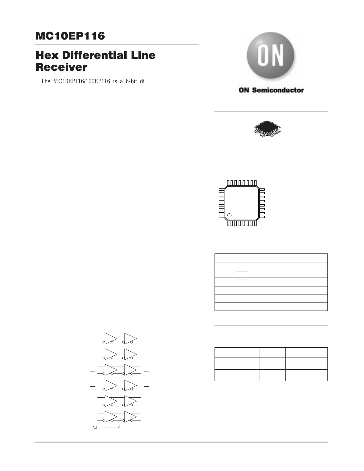
MC10EP116
Hex Differential Line
Receiver
The MC10EP116/100EP116 is a 6-bit differential line receiver
based on the EP16 device. The 3.0GHz bandwidth provided by the
high frequency outputs makes the device ideal for buffering of very
high speed oscillators.
A VBB pin is available to AC couple an input signal to the device.
More information on AC coupling can be found in the design
handbook interfacing with ECLinPS on our website.
The design incorporates two stages of gain, internal to the device,
making it an excellent choice for use in high bandwidth amplifier
applications.
The differential inputs have internal clamp structures which will
force the Q output of a gate in an open input condition to go to a LOW
state. Thus, inputs of unused gates can be left open and will not affect
the operation of the rest of the device. Note that the input clamp will
take affect only if both inputs fall 2.5V below VCC. All VCC and V
pins must be externally connected to power supply to guarantee proper
operation.
• 230ps Typical Propagation Delay
• High Bandwidth to 3.0 GHz Typical
• PECL mode: 3.0V to 5.5V V
• ECL mode: 0V V
with VEE = –3.0V to –5.5V
CC
with VEE = 0V
CC
• Internal Input Resistors: Pulldown on D, Pulldown and Pullup on D
• Q Output will default LOW with inputs open or at V
EE
• ESD Protection: 2KV HBM, 100V MM
• V
BB
Output
• New Differential Input Common Mode Range
• Moisture Sensitivity Level 2
For Additional Information, See Application Note AND8003/D
• Flammability Rating: UL–94 code V–0 @ 1/8”,
Oxygen Index 28 to 34
• Transistor Count: 729 devices
EE
http://onsemi.com
32–LEAD TQFP
FA SUFFIX
CASE 873A
MARKING DIAGRAM*
MC10
EP116
AWLYYWW
32
1
*For additional information, see Application Note
AND8002/D
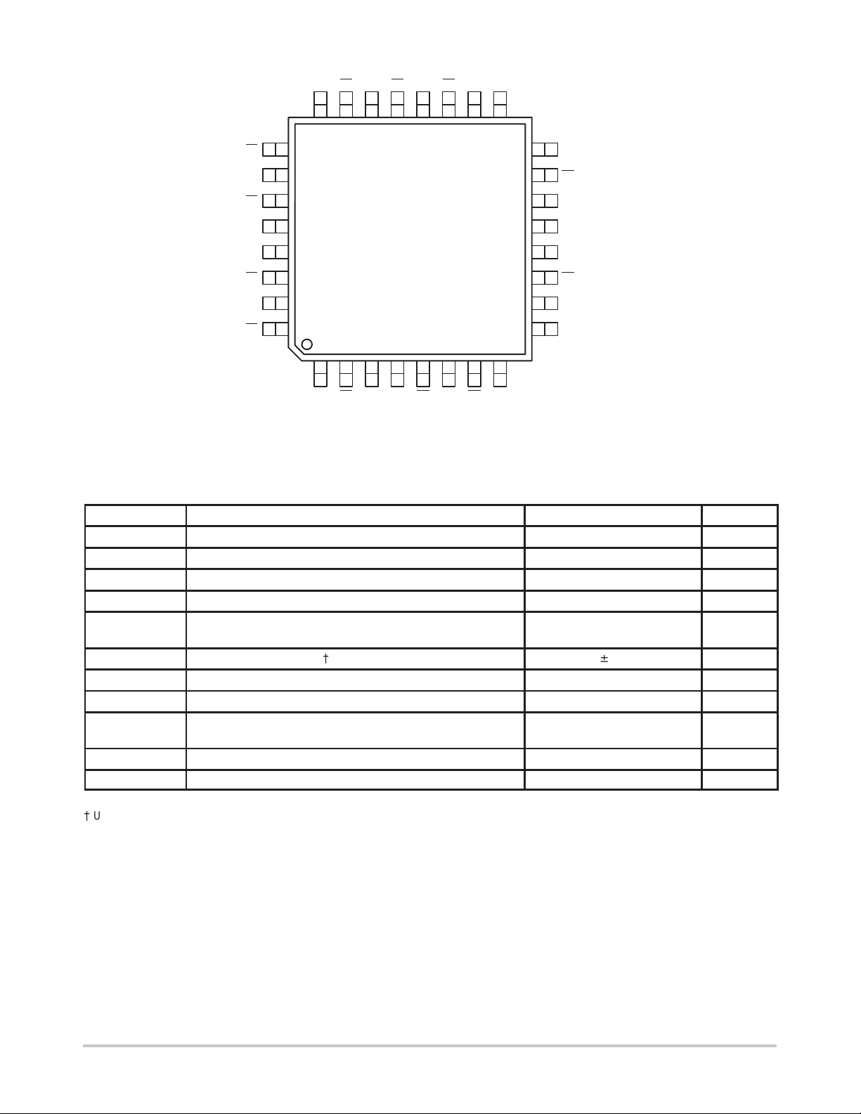
PIN DESCRIPTION
PIN
D[0:5], D[0:5]
Q[0:5], Q[0:5] ECL Differential Data Outputs
VBB
VCC Positive Supply
VEE Negative, 0 Supply
A = Assembly Location
WL = Wafer Lot
YY = Year
WW = Work Week
FUNCTION
ECL Differential Data Inputs
Reference Voltage Output
LOGIC DIAGRAM
D
0
D
0
D
1
D
1
D
2
D
2
D
3
D
3
D
4
D
4
D
5
D
5
V
BB
Semiconductor Components Industries, LLC, 2000
March, 2000 – Rev . 3
Q
0
Q
0
Q
1
Q
1
Q
2
Q
2
Q
3
Q
3
Q
4
Q
4
Q
5
Q
5
1 Publication Order Number:
MC10EP1 16FA TQFP 250 Units/Tray
MC10EP1 16FAR2 TQFP 2000 Tape & Reel
ORDERING INFORMATION
Device Package Shipping
MC10EP116/D
D4
D3
D3
VEE
D2
D2
D1
D1
MC10EP116
24 23 22 21 20 19 18 17
25
26
27
28
MC10EP116
29
30
31
32
12345678
VCCQ4Q4Q5Q5D5D4 D5
16
15
14
13
12
11
10
9
VCC
Q3
Q3
VCC
VCC
Q2
Q2
VCC
D0
VEEQ1Q1Q0Q0VBBD0
Figure 1. 32–Lead LQFP Pinout (Top View)
Warning: All VCC and VEE pins must be externally connected
to Power Supply to guarantee proper operation.
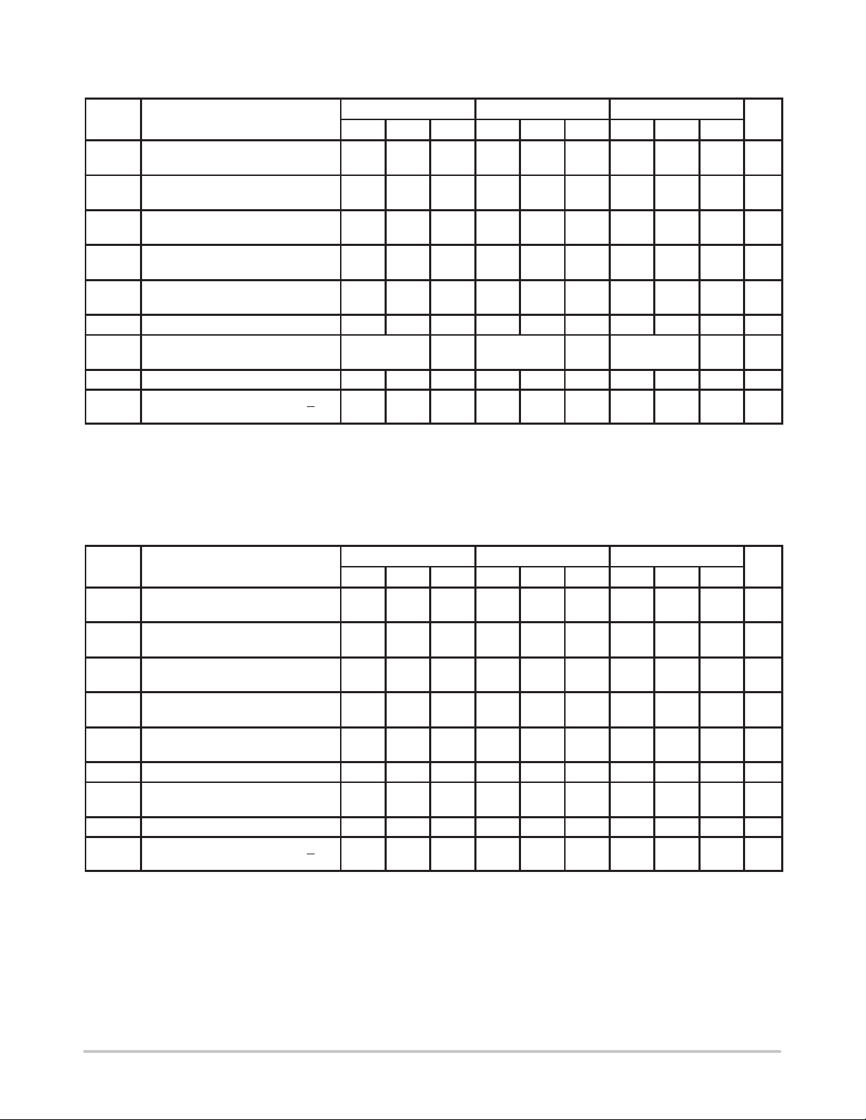
MAXIMUM RATINGS*
Symbol Parameter Value Unit
V
EE
V
CC
V
I
V
I
I
out
I
BB
T
A
T
stg
θ
JA
θ
JC
T
sol
* Maximum Ratings are those values beyond which damage to the device may occur.
{
Use for inputs of same package only.
Power Supply (VCC = 0V) –6.0 to 0 VDC
Power Supply (VEE = 0V) 6.0 to 0 VDC
Input Voltage (VCC = 0V, VI not more negative than VEE) –6.0 to 0 VDC
Input Voltage (VEE = 0V, VI not more positive than VCC) 6.0 to 0 VDC
Output Current Continuous
VBB Sink/Source Current
Operating Temperature Range –40 to +85 °C
Storage Temperature –65 to +150 °C
Thermal Resistance (Junction–to–Ambient) Still Air
Thermal Resistance (Junction–to–Case) 12 to 17 °C/W
Solder Temperature (<2 to 3 Seconds: 245°C desired) 265 °C
{
Surge
500lfpm
50
100
± 0.5 mA
80
55
mA
°C/W
http://onsemi.com
2
MC10EP116
DC CHARACTERISTICS, ECL/LVECL (VCC = 0V; VEE = –5.5V to –3.0V) (Note 4.)
–40°C 25°C 85°C
Symbol Characteristic Min Typ Max Min Typ Max Min Typ Max Unit
IEE
V
OH
V
OL
V
IH
V
IL
V
BB
V
IHCMR
I
IH
I
IL
NOTE: 10EP circuits are designed to meet the DC specifications shown in the above table after thermal equilibrium has been established. The
1. VCC = 0V, VEE = V
2. All loading with 50 ohms to VCC–2.0 volts.
3. V
4. Input and output parameters vary 1:1 with VCC.
Power Supply Current
(Note 1.)
Output HIGH Voltage
(Note 2.)
Output LOW Voltage
(Note 2.)
Input HIGH Voltage
Single Ended
Input LOW Voltage
Single Ended
Output Voltage Reference –1575 –1475 –1375 –1540 –1440 –1340 –1515 –1415 –1315 mV
Input HIGH Voltage Common Mode
Range (Note 3.)
Input HIGH Current 150 150 150 µA
Input LOW Current D
circuit is in a test socket or mounted on a printed circuit board and transverse airflow greater than 500lfpm is maintained.
min varies 1:1 with VEE, max varies 1:1 with VCC.
IHCMR
EEmin
to V
EEmax
D
, all other pins floating.
55 95 55 80 95 55 95 mA
–1135 –1060 –885 –1070 –945 –820 –1010 –885 –760 mV
–1995 –1810 –1685 –1995 –1745 –1620 –1995 –1685 –1560 mV
–1210 –885 –1145 –820 –1085 –760 mV
–1935 –1610 –1870 –1545 –1810 –1485 mV
VEE+2.0 0.0 VEE+2.0 0.0 VEE+2.0 0.0 V
0.5
–150
0.5
–150
0.5
–150
µA
DC CHARACTERISTICS, LVPECL (VCC = 3.3V ± 0.3V, VEE = 0V) (Note 8.)
–40°C 25°C 85°C
Symbol Characteristic Min Typ Max Min Typ Max Min Typ Max Unit
IEE
V
OH
V
OL
V
IH
V
IL
V
BB
V
IHCMR
I
IH
I
IL
NOTE: 10EP circuits are designed to meet the DC specifications shown in the above table after thermal equilibrium has been established. The
5. VCC = 3.0V, VEE = 0V, all other pins floating.
6. All loading with 50 ohms to VCC–2.0 volts.
7. V
8. Input and output parameters vary 1:1 with VCC.
Power Supply Current
(Note 5.)
Output HIGH Voltage
(Note 6.)
Output LOW Voltage
(Note 6.)
Input HIGH Voltage
Single Ended
Input LOW Voltage
Single Ended
Output Voltage Reference 1725 1825 1925 1760 1860 1960 1785 1885 1985 mV
Input HIGH Voltage Common Mode
Range (Note 7.)
Input HIGH Current 150 150 150 µA
Input LOW Current D
circuit is in a test socket or mounted on a printed circuit board and transverse airflow greater than 500lfpm is maintained.
min varies 1:1 with VEE, max varies 1:1 with VCC.
IHCMR
D
55 95 55 80 95 55 95 mA
2165 2240 2415 2230 2355 2480 2290 2415 2540 mV
1305 1490 1615 1305 1555 1680 1305 1615 1740 mV
2090 2415 2155 2480 2215 2540 mV
1365 1690 1430 1755 1490 1815 mV
2.0 3.3 2.0 3.3 2.0 3.3 V
0.5
–150
0.5
–150
0.5
–150
µA
http://onsemi.com
3
 Loading...