


 Loading...
MITSUBISHI MICROCOMPUTERS
M37702M2LXXXGP, M37702S1LGP M37702M2LXXXHP, M37702S1LHP
SINGLE-CHIP 16-BIT CMOS MICROCOMPUTER
DESCRIPTION
The M37702M2LXXXGP is a single-chip 16-bit microcomputer designed with high-performance CMOS silicon gate technology. This is housed in a small 80-pin plastic molded QFP. This singlechip microcomputer has a large 16 M bytes address space, three instruction queue buffers, and two data buffers for high-speed instruction execution. The CPU is a 16-bit parallel processor that can also be switched to perform 8-bit parallel processing. This microcomputer is suitable for communication, office, business and industrial equipment controller that require high-speed processing of large data.
The strong points of the M37702M2LXXXGP, M37702S1LGP, M37702M2LXXXHP and M37702S1LHP are the low supply voltage and small package.
The differences between M37702M2LXXXGP, M37702S1LGP, M37702M2LXXXHP and M37702S1LHP are the ROM size and the package as shown below. Therefore, the following descriptions will be for the M37702M2LXXXGP unless otherwise noted.
Type name |
ROM size |
Package |
|
|
|
M37702M2LXXXGP |
16 K bytes |
80-pin plastic molded QFP (80P6S-A) |
|
|
|
M37702S1LGP |
External |
80-pin plastic molded QFP (80P6S-A) |
|
|
|
M37702M2LXXXHP |
16 K bytes |
80-pin plastic molded fine-pitch QFP (80P6D-A) |
|
|
|
M37702S1LHP |
External |
80-pin plastic molded fine-pitch QFP (80P6D-A) |
FEATURES
∙ Number of basic instructions .................................................. |
103 |
|
∙ Memory size |
ROM ................................................ |
16 K bytes |
|
RAM ................................................. |
512 bytes |
∙ Instruction execution time |
|
|
The fastest instruction at 8 MHz frequency ....................... |
500 ns |
|
∙ Single low supply voltage ........................................... |
2.7 – 5.5 V |
|
∙ Low power dissipation |
|
|
(At 3 V supply voltage, 8 MHz frequency) .............. |
12 mW (Typ.) |
|
(At 5 V supply voltage, 8 MHz frequency) .............. |
30 mW (Typ.) |
|
∙ Wide operating temperature range ............................. |
–40 – 80°C |
|
∙ Interrupts ............................................................ |
|
19 types 7 levels |
∙ Multiple function 16-bit timer ................................................ |
5 + 3 |
|
∙ UART (may also be synchronous) .............................................. |
2 |
|
∙ 8-bit A-D converter ............................................. |
8-channel inputs |
|
∙12-bit watchdog timer
∙Programmable input/output
(ports P0, P1, P2, P3, P4, P5, P6, P7, P8) .............................. |
68 |
∙ Small package |
|
M37702M2LXXXGP, M37702S1LGP |
|
.................................................. 80-pin QFP (0.65 mm lead pitch) M37702M2LXXXHP, M37702S1LHP
.................................... 80-pin fine-pitch QFP (0.5 mm lead pitch)
APPLICATION
Control devices for communication equipment such as cellular radio telephones, cordless telephones, and radio communications Control devices for office equipment such as copiers, printers, typewriters, facsimiles, word processors, and personal computers Control devices for industrial equipments such as ME, NC, and measuring instruments
NOTE
Refer to “Chapter 5 PRECAUTIONS” when using this microcomputer.

MITSUBISHI MICROCOMPUTERS
M37702M2LXXXGP, M37702S1LGP
M37702M2LXXXHP, M37702S1LHP
SINGLE-CHIP 16-BIT CMOS MICROCOMPUTER
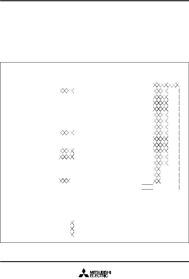
PIN CONFIGURATION (TOP VIEW)
|
|
|
|
|
|
|
|
|
|
|
|
|
|
|
/RXD1 |
/TXD1 |
|
/A0 |
|
/A1 |
|
/A2 |
|
/A3 |
/A4 |
/A5 |
/A6 |
|
/A7 |
|
/A8/D8 |
/A9/D9 |
/A10/D10 |
/A11/D11 |
/A12/D12 |
|
/A13/D13 |
/A14/D14 |
/A15/D15 |
/A16/D0 |
/A17/D1 |
|
|
|
|
|
|
|
|
|
|
|
|
|
||||||||||||||
|
|
|
|
|
|
|
|
|
|
|
|
|
|
|
P86 |
P87 |
|
P00 |
|
P01 |
|
P02 |
|
P03 |
P04 |
P05 |
P06 |
|
P07 |
|
P10 |
P11 |
P12 |
P13 |
P14 |
|
P15 |
P16 |
P17 |
P20 |
P21 |
|
|
|
|
|
|
|
|
|
|
|
|
|
||||||||||||||
|
|
|
|
|
|
|
|
|
|
|
|
|
|
|
|
|
|
|
|
|
|
|
|
|
|
|
|
|
|
|
|
|
|
|
|
|
|
|
|
|
|
|
|
|
|
|
|
|
|
|
|
|
|
|
|
|
|
|
|
|
|
|
|
|
|
|
|
|
|
|
|
|
|
|
|
|
|
|
|
|
|
|
|
60 |
|
59 |
|
58 |
|
57 |
|
56 |
|
55 |
|
54 |
|
53 |
|
52 |
|
51 |
|
50 |
|
49 |
|
48 |
|
47 |
|
46 |
|
45 |
|
44 |
|
43 |
|
42 |
|
41 |
|
|
|
|
|
|
|
|
|
|
|
|
|
|
|
|
|
P85/CLK1 |
|
|
|
|
|
|
|
|
|
|
|
|
|
|
|
|
|
|
|
|
|
|
|
|
|
|
|
|
|
|
|
|
|
|
|
|
|
|
|
|
|
|
|
|
|
|
|
P22/A18/D2 |
||||||||||||||||||
|
61 |
|
|
|
|
|
|
|
|
|
|
|
|
|
|
|
|
|
|
|
|
|
|
|
|
|
|
|
|
|
|
|
|
|
|
|
|
|
|
|
|
40 |
||||||||||||||||||||||||||
P84 |
|
|
|
|
|
|
|
|
|
|
|
|
|
|
|
|
|
|
|
|
|
|
|
|
|
|
|
|
|
|
|
|
|
|
|
|
|
|
|
|
|
|
|
|
|
|
|
|
|
|
|
|
P23/A19/D3 |
|||||||||||||||
/CTS1/RTS1 |
|
62 |
|
|
|
|
|
|
|
|
|
|
|
|
|
|
|
|
|
|
|
|
|
|
|
|
|
|
|
|
|
|
|
|
|
|
|
|
|
|
|
|
39 |
|
|
|
|
|||||||||||||||||||||
|
|
P83/TXD0 |
|
|
|
|
|
|
|
|
|
|
|
|
|
|
|
|
|
|
|
|
|
|
|
|
|
|
|
|
|
|
|
|
|
|
|
|
|
|
|
|
|
|
|
|
|
|
|
|
P24/A20/D4 |
|||||||||||||||||
|
|
|
63 |
|
|
|
|
|
|
|
|
|
|
|
|
|
|
|
|
|
|
|
|
|
|
|
|
|
|
|
|
|
|
|
|
|
|
|
|
|
|
|
|
38 |
|
|
|
|
||||||||||||||||||||
|
|
P82/RXD0 |
|
|
|
|
|
|
|
|
|
|
|
|
|
|
|
|
|
|
|
|
|
|
|
|
|
|
|
|
|
|
|
|
|
|
|
|
|
|
|
|
|
|
|
|
|
|
|
|
|
P25/A21/D5 |
||||||||||||||||
|
|
64 |
|
|
|
|
|
|
|
|
|
|
|
|
|
|
|
|
|
|
|
|
|
|
|
|
|
|
|
|
|
|
|
|
|
|
|
|
|
|
|
|
37 |
|
|
|
|
|||||||||||||||||||||
|
|
P81/CLK0 |
|
|
|
|
|
|
|
|
|
|
|
|
|
|
|
|
|
|
|
|
|
|
|
|
|
|
|
|
|
|
|
|
|
|
|
|
|
|
|
|
|
|
|
|
|
|
|
|
P26/A22/D6 |
|||||||||||||||||
|
65 |
|
|
|
|
|
|
|
|
|
|
|
|
|
|
|
|
|
|
|
|
|
|
|
|
|
|
|
|
|
|
|
|
|
|
|
|
|
|
|
|
36 |
||||||||||||||||||||||||||
P80 |
|
|
|
|
|
|
|
|
|
|
|
|
|
|
|
|
|
|
|
|
|
|
|
|
|
|
|
|
|
|
|
|
|
|
|
|
|
|
|
|
|
|
|
|
|
|
|
|
|
|
|
|
|
|
|
P27/A23/D7 |
||||||||||||
/CTS0/RTS0 |
|
66 |
|
|
|
|
|
|
|
|
|
|
|
|
|
|
|
|
|
|
|
|
|
|
|
|
|
|
|
|
|
|
|
|
|
|
|
|
|
|
|
|
35 |
|||||||||||||||||||||||||
|
|
|
|
|
|
VCC |
|
|
|
|
|
|
|
|
|
|
|
|
|
M37702M2LXXXGP |
|
|
|
|
|
|
|
|
|
|
|
|
|
|
|
|
|
|
|
|
|
|
|
|
|
|||||||||||||||||||||||
|
|
|
|
|
|
|
67 |
|
|
|
|
|
|
|
|
|
|
|
|
|
|
|
|
|
|
|
|
|
34 |
|
|
|
|
P30/R/W |
||||||||||||||||||||||||||||||||||
|
|
|
|
|
AVCC |
|
|
|
|
|
|
|
|
|
|
|
|
|
|
|
|
|
|
|
|
|
|
|
|
|
|
|
|
|
|
|||||||||||||||||||||||||||||||||
|
|
|
|
|
|
|
68 |
|
|
|
|
|
|
|
|
|
|
|
|
|
|
|
|
|
|
|
or |
|
|
|
|
|
|
|
|
|
|
|
|
|
|
|
|
|
|
33 |
|
|
|
|
P31/ |
BHE |
|
|
|
|||||||||||||
|
|
|
|
|
|
VREF |
|
|
|
|
|
|
|
|
|
|
|
|
|
|
|
|
|
|
|
|
|
|
|
|
|
|
|
|
|
|
|
|
|
|
|
|
|
|
|
|
|
|
|
|
|
|
|
|
|
|
P32/ALE |
|||||||||||
|
|
69 |
|
|
|
|
|
|
|
|
|
|
|
|
|
M37702S1LGP |
|
|
|
|
|
|
|
|
|
|
|
32 |
|
|
|
|
||||||||||||||||||||||||||||||||||||
|
|
|
|
|
AVSS |
|
|
|
|
|
|
|
|
|
|
|
|
|
|
|
|
|
|
|
|
|
|
|
|
|
|
|
|
|
|
|
|
|||||||||||||||||||||||||||||||
|
|
|
|
|
|
70 |
|
|
|
|
|
|
|
|
|
|
|
|
|
|
|
|
|
|
|
|
|
|
|
|
|
|
|
|
|
|
|
|
|
|
|
|
|
|
|
|
31 |
|
|
|
|
|
|
|
|
|
|
|
|
|
||||||||
|
|
|
|
|
|
|
|
|
|
|
|
|
|
|
|
|
|
|
|
|
|
|
|
|
or |
|
|
|
|
|
|
|
|
|
|
|
|
|
|
|
|
|
|
|
|
P33/HLDA |
||||||||||||||||||||||
|
|
|
|
|
|
VSS |
|
|
|
|
|
|
|
|
|
|
|
|
|
|
|
|
|
|
|
|
|
|
|
|
|
|
|
|
|
|
|
|
|
|
|
|
|
|
|
|
|
|
|
|
||||||||||||||||||
|
|
|
|
|
|
|
71 |
|
|
|
|
|
|
|
|
|
|
|
M37702M2LXXXHP |
|
|
|
|
|
|
|
|
|
|
30 |
|
|
|
|
Vss |
|||||||||||||||||||||||||||||||||
|
|
|
|
|
|
|
|
|
|
|
|
|
|
|
|
|
|
|
|
|
|
|
|
|
|
|
|
|
|
|
|
|
|
|
|
|
|
|
|
|
|
|
|
|
|
|
|
|
|
|||||||||||||||||||
P77/AN7/ADTRG |
|
72 |
|
|
|
|
|
|
|
|
|
|
|
|
|
|
|
|
|
|
|
or |
|
|
|
|
|
|
|
|
|
|
|
|
|
|
|
|
|
29 |
|
|
|
|
E |
|||||||||||||||||||||||
|
|
P76/AN6 |
|
|
|
|
|
|
|
|
|
|
|
|
|
|
|
|
|
|
|
|
|
|
|
|
|
|
|
|
|
|
|
|
|
|
|
|
|
|
|
|
|
|
|
|
XOUT |
|||||||||||||||||||||
|
|
|
73 |
|
|
|
|
|
|
|
|
|
|
|
|
|
M37702S1LHP |
|
|
|
|
|
|
|
|
|
|
|
28 |
|
|
|
|
|||||||||||||||||||||||||||||||||||
|
|
P75/AN5 |
|
|
|
|
|
|
|
|
|
|
|
|
|
|
|
|
|
|
|
|
|
|
|
|
|
|
|
|
|
|
|
|
XIN |
|||||||||||||||||||||||||||||||||
|
|
|
74 |
|
|
|
|
|
|
|
|
|
|
|
|
|
|
|
|
|
|
|
|
|
|
|
|
|
|
|
|
|
|
|
|
|
|
|
|
|
|
|
|
27 |
|
|
|
|
||||||||||||||||||||
|
|
P74/AN4 |
|
|
|
|
|
|
|
|
|
|
|
|
|
|
|
|
|
|
|
|
|
|
|
|
|
|
|
|
|
|
|
|
|
|
|
|
|
|
|
|
|
|
|
|
|
|
|
|
|
|
|
|
|
|
|
|
|
|||||||||
|
|
|
75 |
|
|
|
|
|
|
|
|
|
|
|
|
|
|
|
|
|
|
|
|
|
|
|
|
|
|
|
|
|
|
|
|
|
|
|
|
|
|
|
|
26 |
|
|
|
|
RESET |
|||||||||||||||||||
|
|
P73/AN3 |
|
|
|
|
|
|
|
|
|
|
|
|
|
|
|
|
|
|
|
|
|
|
|
|
|
|
|
|
|
|
|
|
|
|
|
|
|
|
|
|
|
|
|
|
|
|
|
|
CNVSS |
|||||||||||||||||
|
|
|
76 |
|
|
|
|
|
|
|
|
|
|
|
|
|
|
|
|
|
|
|
|
|
|
|
|
|
|
|
|
|
|
|
|
|
|
|
|
|
|
|
|
25 |
|
|
|
|
||||||||||||||||||||
|
|
P72/AN2 |
|
|
|
|
|
|
|
|
|
|
|
|
|
|
|
|
|
|
|
|
|
|
|
|
|
|
|
|
|
|
|
|
|
|
|
|
|
|
|
|
|
|
|
|
|
|
|
BYTE |
||||||||||||||||||
|
|
77 |
|
|
|
|
|
|
|
|
|
|
|
|
|
|
|
|
|
|
|
|
|
|
|
|
|
|
|
|
|
|
|
|
|
|
|
|
|
|
|
|
24 |
|
|
|
|
|||||||||||||||||||||
|
|
|
|
|
|
|
|
|
|
|
|
|
|
|
|
|
|
|
|
|
|
|
|
|
|
|
|
|
|
|
|
|
|
|
|
|
|
|
|
|
|
|
|
|
||||||||||||||||||||||||
|
|
|
|
|
|
|
|
|
|
|
|
|
|
|
|
|
|
|
|
|
|
|
|
|
|
|
|
|
|
|
|
|
|
|
|
|
|
|
|
|
|
|
|
|
|
|
|
|
|
|
|
|
|
|
|
|
|
|
|
|
|
|
|
|
|
|
|
|
|
|
P71/AN1 |
|
78 |
|
|
|
|
|
|
|
|
|
|
|
|
|
|
|
|
|
|
|
|
|
|
|
|
|
|
|
|
|
|
|
|
|
|
|
|
|
|
|
|
23 |
|
|
|
|
P40/ |
HOLD |
|
||||||||||||||||
|
|
|
|
|
|
|
|
|
|
|
|
|
|
|
|
|
|
|
|
|
|
|
|
|
|
|
|
|
|
|
|
|
|
|
|
|
|
|
|
|
|
|
|
|
|
|
|
|
|
|
|
|
|
|
|
|||||||||||||
|
|
P70/AN0 |
|
79 |
|
|
|
|
|
|
|
|
|
|
|
|
|
|
|
|
|
|
|
|
|
|
|
|
|
|
|
|
|
|
|
|
|
|
|
|
|
|
|
|
22 |
|
|
|
|
P41/RDY |
||||||||||||||||||
|
|
P67/TB2IN |
|
|
|
|
|
|
|
|
|
|
|
|
|
|
|
|
|
|
|
|
|
|
|
|
|
|
|
|
|
|
|
|
|
|
|
|
|
|
|
|
|
|
|
|
|
|
|
|
P42/φ1 |
|||||||||||||||||
|
80 |
|
|
|
|
|
|
|
|
|
|
|
|
|
|
|
|
|
|
|
|
|
|
|
|
|
|
|
|
|
|
|
|
|
|
|
|
|
|
|
|
21 |
|
|
|
|
||||||||||||||||||||||
|
|
|
|
|
|
|
|
|
|
|
|
|
|
|
|
|
|
|
|
|
|
|
|
|
|
|
|
|
|
|
|
|
|
|
|
|
|
|
|
|
|
|
|
|
|
|
|
|
|
|
|
|
|
|
|
|
|
|
|
|
|
|
|
|
|
|
|
|
|
|
|
|
|
|
|
|
|
|
|
|
|
|
|
1 |
|
2 |
|
3 |
|
4 |
|
5 |
|
6 |
|
7 |
|
8 |
|
9 |
|
10 |
|
11 |
|
12 |
|
13 |
|
14 |
|
15 |
|
16 |
|
17 |
|
18 |
|
19 |
|
20 |
|
|
|
|
|
|
|
|
|
|
|
|
|
|
|
|
|
|
|
|
|
|
|
|
|
|
|
|
|
|
|
|
|
|
|
|
|
|
|
|
|
|
|
|
|
|
|
|
|
|
|
|
|
|
P45/VDA |
P44/QCL |
P43/MX |
|
|
|
|
|
|
|
|
|
|
|
|
|
||||||||||||||
|
|
|
|
|
|
|
|
|
|
|
|
|
|
|
P66/TB1IN |
P65/TB0IN |
|
P64/INT2 |
|
P63/INT1 |
|
P62/INT0 |
|
P61/TA4IN |
P60/TA4OUT |
P57/TA3IN |
P56/TA3OUT |
|
P55/TA2IN |
|
P54/TA2OUT |
P53/TA1IN |
P52/TA1OUT |
P51/TA0IN |
P50/TA0OUT |
|
P47/DBC |
P46/VPA |
|
|
|
|
|
|
|
|
|
|
|
|
|
|||||||||||||||||
|
|
|
|
|
|
|
|
|
|
|
|
|
|
|
|
|
|
|
|
|
|
|
|
|
|
|
|
|
|
|
|
|
|
|
||||||||||||||||||||||||||||||||||
|
|
|
|
|
|
|
|
|
|
|
|
|
|
|
|
|
|
|
|
|
|
|
|
|
|
|
|
|
|
|
|
|
|
|
||||||||||||||||||||||||||||||||||
Outline
M37702M2LXXXGP, M37702S1LGP••••••80P6S-A
M37702M2LXXXHP, M37702S1LHP••••••80P6D-A
: Used in the evaluation chip mode only
2

MITSUBISHI MICROCOMPUTERS
M37702M2LXXXGP, M37702S1LGP M37702M2LXXXHP, M37702S1LHP
SINGLE-CHIP 16-BIT CMOS MICROCOMPUTER
Bus width |
selection input |
|
BYTE |
24 |
|
|
|
|
|
|
|
|
|
|
|
|
|
|
|
|
|
|
|
|
|
|
|
|
|
Reference |
voltage input |
VREF |
69 |
|
|
|
|
|
|
|
Instruction Register(8) |
|
|
|
|
|
|
|
|
|
|||||||||
|
AVCC |
|
|
|
|
|
|
|
|
|
|
|||
|
|
|
|
|
|
|
|
|
|
|
||||
|
|
|
|
|
|
|
|
|
|
|
||||
|
|
|
|
|
|
|
|
|
|
|
||||
|
(5V) |
|
68 |
|
|
|
|
|
|
|
|
|
|
|
|
|
|
|
|
|
|
|
|
|
|
|
|||
|
(0V) |
|
AVSS |
70 |
|
|
|
|
|
|
|
|
|
|
|
|
|
|
|
|
|
|
|
|
|
|
|||
|
(0V) |
CNVss |
25 |
|
|
|
|
|
|
|
|
|
|
|
|
|
|
|
|
|
|
|
|
|
|||||
|
(0V) |
|
VSS |
30 71 |
|
|
|
|
|
|
|
|
|
|
|
|
|
|
|
|
|
|
|
|
|
|
|||
|
|
|
|
|
|
|
|
|
|
|
|
|||
|
(5V) |
|
VCC |
67 |
|
|
|
|
|
|
|
|
|
|
|
|
|
|
|
|
|
|
|
|
|
|
|||
M37702M2LXXXGP BLOCK DIAGRAM |
Reset input |
|
RESET |
26 |
|
|
|
|
|
|
|
|
|
|
|
|
|
|
|
|
|
|
|
|
|
||||
|
|
|
|
|
|
|
|
|
||||||
|
|
|
|
|
|
|
|
|
|
|
|
|
||
Clock input Clock output Enable output |
|
XIN XOUT E |
27 28 29 |
|
|
|
|
|
|
|
|
|
|
|
|
|
|
|
|
|
|
Clock Generating Circuit |
|
||||||
|
|
|
|
|
|
|
|
|||||||
|
|
|
|
|
||||||||||
|
|
|
|
|
|
|
|
|||||||
|
|
|
|
|
|
|
|
|
|
|
|
|
||
Data Buffer DBH(8)
Data Buffer DBL(8)
Instruction Queue Buffer Q0(8)
Instruction Queue Buffer Q1(8)
Instruction Queue Buffer Q2(8)
Incrementer(24)

 Program Address Register PA(24)
Data Address Register DA(24)
Incrementer/Decrementer(24) |
Program Counter PC(16) |
Program Bank Register PG(8) |
Data Bank Register DT(8) |
Input Buffer Register IB(16)

 Processor Status Register PS(11)
Direct Page Register DPR(16)
Stack Pointer S(16)
Index Register Y(16)
Index Register X(16)
Accumulator B(16)
Accumulator A(16)
Arithmetic Logic
Unit(16)
|
Data Bus(Even) |
|
|
|
|
|||
|
Data Bus(Odd) |
|
|
|
|
|||
|
|
|
|
|
P0(8) |
52 53 54 55 56 57 58 |
Input/Output |
port P0 |
|
|
|
|
|
|
51 |
|
|
|
|
|
|
|
|
50 |
Input/Output |
portP1 |
Address Bus |
|
|
P1(8) |
46454447 48 49 |
||||
|
|
|
|
|
|
|||
|
|
|
|
|
|
43 |
|
|
|
|
|
|
|
P2(8) |
36 37 38 39 40 41 42 |
Input/Output |
port P2 |
|
|
|
|
|
|
35 |
|
|
|
|
|
|
A-D Converter(8) |
P3(4) |
31 32 33 34 |
Input/Output |
port P3 |
|
|
|
UART1(9) |
UART0(9) |
P4(8) |
17 18 19 20 21 22 23 |
Input/Output |
port P4 |
|
|
|
|
|
|
16 |
|
|
|
Watchdog Timer |
Timer TB2(16) |
Timer TB1(16) |
Timer TB0(16) |
P5(8) |
8 9 10 11 12 13 14 15 |
Input/Output |
port P5 |
Timer TA4(16) |
Timer TA3(16) |
Timer TA2(16) |
Timer TA1(16) |
Timer TA0(16) |
|
7 |
|
|
P6(8) |
80 1 2 3 4 5 6 |
Input/Output |
port P6 |
|||||
|
|
RAM |
|
512 Bytes |
P7(8) |
73 74 75 76 77 78 79 |
Input/Output |
port P7 |
|
|
|
|
|
|
72 |
|
|
|
|
ROM |
|
16K Bytes |
P8(8) |
60 61 62 63 64 65 66 |
Input/Output |
port P8 |
|
|
|
|
|
|
59 |
|
|
3

MITSUBISHI MICROCOMPUTERS
M37702M2LXXXGP, M37702S1LGP
M37702M2LXXXHP, M37702S1LHP
SINGLE-CHIP 16-BIT CMOS MICROCOMPUTER
FUNCTIONS OF M37702M2LXXXGP
Parameter |
Functions |
|||
|
|
|
|
|
Number of basic instructions |
103 |
|||
|
|
|
|
|
Instruction execution time |
500 ns (the fastest instruction at external clock 8 MHz frequency) |
|||
|
|
|
|
|
Memory size |
|
ROM |
16 K bytes |
|
|
|
|||
|
RAM |
512 bytes |
||
|
|
|||
|
|
|
|
|
Input/Output ports |
|
P0 – P2, P4 – P8 |
8-bit 8 |
|
|
|
|||
|
P3 |
4-bit 1 |
||
|
|
|||
|
|
|
|
|
Multi-function timers |
|
TA0, TA1, TA2, TA3, TA4 |
16-bit 5 |
|
|
TB0, TB1, TB2 |
16-bit 3 |
||
|
|
|||
Serial I/O |
(UART or clock synchronous serial I/O) 2 |
|||
A-D converter |
8-bit 1 (8 channels) |
|||
Watchdog timer |
12-bit 1 |
|||
Interrupts |
3 external types, 16 internal types |
|||
(Each interrupt can be set the priority levels to 0 – 7.) |
||||
|
|
|
||
|
|
|
|
|
Clock generating circuit |
Built-in (externally connected to a ceramic resonator or quartz |
|||
crystal resonator) |
||||
|
|
|
||
|
|
|
|
|
Supply voltage |
2.7 – 5.5 V |
|||
|
|
|
|
|
Power dissipation |
12 mW (at 3 V supply voltage, external clock 8 MHz frequency) |
|||
|
||||
30 mW (at 5 V supply voltage, external clock 8 MHz frequency) |
||||
|
|
|
||
|
|
|
|
|
Input/Output characteristic |
|
Input/Output voltage |
5 V |
|
|
|
|
||
Output current |
5 mA |
|||
|
|
|||
Memory expansion |
Maximum 16 M bytes |
|||
Operating temperature range |
–40 – 85°C |
|||
Device structure |
CMOS high-performance silicon gate process |
|||
Package |
|
M37702M2LXXXGP, M37702S1LGP |
80-pin plastic molded QFP (80P6S-A: 0.65 mm lead pitch) |
|
|
M37702M2LXXXHP, M37702S1LHP |
80-pin plastic molded fine-pitch QFP (80P6D-A: 0.5 mm lead pitch) |
||
|
|
|||
4

MITSUBISHI MICROCOMPUTERS
M37702M2LXXXGP, M37702S1LGP
M37702M2LXXXHP, M37702S1LHP
SINGLE-CHIP 16-BIT CMOS MICROCOMPUTER
PIN DESCRIPTION
Pin |
Name |
Input/Output |
Functions |
|
|
|
|
VCC, VSS |
Power supply |
|
Supply 2.7 – 5.5 V to VCC and 0 V to VSS. |
|
|
|
|
CNVSS |
CNVSS input |
Input |
This pin controls the processor mode. Connect to VSS for single-chip mode, and |
|
|
|
to VCC for external ROM types. |
|
|
|
|
______ |
|
|
|
RESET |
Reset input |
Input |
To enter the reset state, this pin must be kept at a “L” condition which should be |
|
|
|
maintained for the required time. |
|
|
|
|
XIN |
Clock input |
Input |
These are I/O pins of internal clock generating circuit. Connect a ceramic or quartz |
|
|
|
crystal resonator between XIN and XOUT. When an external clock is used, the clock |
|
|
|
|
XOUT |
Clock output |
Output |
source should be connected to the XIN pin and the XOUT pin should be left open. |
|
|
|
|
_ |
|
|
|
E |
Enable output |
Output |
Data or instruction read and data write are performed when output from this pin |
|
|
|
is “L”. |
|
|
|
|
BYTE |
Bus width selection |
Input |
In memory expansion mode or microprocessor mode, this pin determines |
|
input |
|
whether the external data bus is 8-bit width or 16-bit width. The width is 16 bits |
|
|
|
when “L” signal inputs and 8 bits when “H” signal inputs. |
|
|
|
|
AVCC, |
Analog supply input |
|
Power supply for the A-D converter. Connect AVCC to VCC and AVSS to VSS |
AVSS |
|
|
externally. |
|
|
|
|
VREF |
Reference voltage |
Input |
This is reference voltage input pin for the A-D converter. |
|
input |
|
|
|
|
|
|
P00 – P07 |
I/O port P0 |
I/O |
In single-chip mode, port P0 becomes an 8-bit I/O port. An I/O direction register |
|
|
|
is available so that each pin can be programmed for input or output. These ports |
|
|
|
are in input mode when reset. |
|
|
|
Address (A7 – A0) is output in memory expansion mode or microprocessor mode. |
|
|
|
|
P10 – P17 |
I/O port P1 |
I/O |
In single-chip mode, these pins have the same functions as port P0. When the |
|
|
|
BYTE pin is set to “L” in memory expansion mode or microprocessor mode and |
|
|
|
external_ data bus is 16-bit width, high-order data (D15 – D8) is_ input or output |
|
|
|
when E output is “L” and an address (A15 – A8) is output when E output is “H”. |
|
|
|
If the BYTE pin is “H” that is an external data bus is 8-bit width, only address |
|
|
|
(A15 – A8) is output. |
|
|
|
|
P20 – P27 |
I/O port P2 |
I/O |
In single-chip mode, these pins have the same functions as port P0. In memory |
|
|
|
expansion mode_ or microprocessor mode low-order data (D7 – D0) is_input or |
|
|
|
output when E output is “L” and an address (A23 – A16) is output when E output |
|
|
|
is “H”. |
|
|
|
|
P30 – P33 |
I/O port P3 |
I/O |
In single-chip mode, these pins have the same__functions____ as port P0._____In memory |
|
|
|
expansion mode or microprocessor mode, R/W, BHE, ALE and HLDA signals |
|
|
|
are output. |
|
|
|
|
P40 – P47 |
I/O port P4 |
I/O |
In single-chip mode, these pins have the same functions as port_____P0. In memory____ |
|
|
|
expansion mode or microprocessor mode, P40 and P41 become HOLD and RDY |
|
|
|
input pin respectively. Functions of other pins are the same as in single-chip |
|
|
|
mode. In single-chip mode or memory expansion mode, port P42 can be pro- |
|
|
|
grammed for φ1 output pin divided the clock to XIN pin by 2. In microprocessor |
|
|
|
mode. P42 always has the function as φ1 output pin. |
|
|
|
|
P50 – P57 |
I/O port P5 |
I/O |
In addition to having the same functions as port P0 in single-chip mode, these |
|
|
|
pins also function as I/O pins for timer A0, timer A1, timer A2 and timer A3. |
|
|
|
|
P60 – P67 |
I/O port P6 |
I/O |
In addition to having the same functions as port P0 in single-chip____mode,____these |
|
|
|
____pins also function as I/O pins for timer A4, external interrupt input INT0, INT1 and |
|
|
|
INT2 pins, and input pins for timer B0, timer B1 and timer B2. |
|
|
|
|
P70 – P77 |
I/O port P7 |
I/O |
In addition to having the same functions as port P0 in single-chip mode, these |
|
|
|
pins also function as analog input AN0 – AN7 input pins. P77 also has an A-D |
|
|
|
conversion trigger input function. |
|
|
|
|
P80 – P87 |
I/O port P8 |
I/O |
In addition to having the same functions____as____port P0 in single-chip mode, these |
|
|
|
pins also function as RXD, TXD, CLK, CTS/RTS pins for UART 0 and UART 1. |
|
|
|
|
|
|
|
|
5
MITSUBISHI MICROCOMPUTERS
M37702M2LXXXGP, M37702S1LGP M37702M2LXXXHP, M37702S1LHP
SINGLE-CHIP 16-BIT CMOS MICROCOMPUTER
BASIC FUNCTION BLOCKS
The M37702M2LXXXGP has the same functions as the M37702M2BXXXFP except for the reset circuit.
Refer to the section on the M37702M2BXXXFP.
Figure 1 shows the status of the internal registers when a reset occurs.
Figure 2 shows an example of a reset circuit. The reset input voltage must be held 0.55 V or lower when the power voltage reaches 2.7 V.
RESET CIRCUIT
______
Reset occurs when the RESET pin is returned to “H” level after holding it at “L” level when the power voltage is at 2.7 – 5.5 V. Program execution starts at the address formed by setting the address pins A23 – A16 to 0016, A15 – A8 to the contents of address FFFF16, and A7 – A0 to the contents of address FFFE16.
|
|
Address |
|
|
|
|
|
|
|
|
|
|
|
Address |
|
|
|
|
|
|
|
|
||||
|
|
|
|
|
|
|
|
|
|
|
|
(5E16)••• |
|
|
|
|
|
|
|
|
||||||
(1) Port P0 data direction register |
(0416)••• |
|
|
|
0016 |
|
|
|
(29) Processor mode register |
0016 |
|
|
|
|||||||||||||
|
|
|
|
|
|
|
|
|
|
|
|
|
|
|
|
|
|
|
|
|
|
|
|
|
||
(2) Port P1 data direction register |
(0516)••• |
|
|
|
0016 |
|
|
|
(30) Watchdog timer |
(6016)••• |
|
|
|
FFF16 |
|
|
|
|||||||||
|
|
|
|
|
|
|
|
|
|
|
|
|
|
|
|
|
|
|
|
|
|
|
|
|
|
|
(3) Port P2 data direction register |
(0816)••• |
|
|
|
0016 |
|
|
|
(31) Watchdog timer frequency selection |
(6116)••• |
|
|
|
|
|
|
|
0 |
||||||||
|
|
|
|
|
|
|
|
|
|
|
|
flag |
|
|
|
|
|
|
|
|
|
|
|
|
|
|
|
|
|
|
|
|
|
|
|
|
|
|
|
|
|
|
|
|
|
|
|
|
|
|
|
||
(4) Port P3 data direction register |
(0916)••• |
|
|
|
|
0 |
0 |
0 |
0 |
(32) |
A-D conversion interrupt control register (7016)••• |
|
|
|
|
0 |
0 |
0 |
0 |
|||||||
|
|
|
|
|
|
|
|
|
|
|
|
|
|
|
|
|
|
|
|
|
|
|
|
|
|
|
|
|
(0C16)••• |
|
|
|
|
|
|
|
|
|
|
|
|
|
|
|
|
|
|
|
|
|
|
|
|
(5) Port P4 data direction register |
|
|
|
0016 |
|
|
|
(33) |
UART 0 transmission interrupt control |
|
(7116)••• |
|
|
|
|
0 |
0 |
0 |
0 |
|||||||
|
|
|
|
|
|
|
|
|
|
|
|
|
register |
|
|
|
|
|
|
|
|
|
|
|
|
|
(6) Port P5 data direction register |
(0D16)••• |
|
|
|
0016 |
|
|
|
(34) |
UART 0 receive interrupt control register (7216)••• |
|
|
|
|
0 |
0 |
0 |
0 |
||||||||
|
|
|
|
|
|
|
|
|
|
|
|
|
|
|
|
|
|
|
|
|
|
|
|
|
|
|
(7) Port P6 data direction register |
(1016)••• |
|
|
|
0016 |
|
|
|
(35) |
UART 1 transmission interrupt control |
|
(7316)••• |
|
|
|
|
0 |
0 |
0 |
0 |
||||||
|
|
|
|
|
|
|
|
|
|
|
|
|
register |
|
|
|
|
|
|
|
|
|
|
|
|
|
|
|
|
|
|
|
|
|
|
|
|
|
|
|
|
|
|
|
|
|
|
|
|
|
|
|
|
(8) Port P7 data direction register |
(1116)••• |
|
|
|
0016 |
|
|
|
(36) |
UART 1 receive interrupt control register (7416)••• |
|
|
|
|
0 |
0 |
0 |
0 |
||||||||
|
|
|
|
|
|
|
|
|
|
|
|
|
|
|
|
|
|
|
|
|
|
|
|
|
|
|
(9) Port P8 data direction register |
(1416)••• |
|
|
|
0016 |
|
|
|
(37) |
Timer A0 interrupt control register |
|
(7516)••• |
|
|
|
|
0 |
0 |
0 |
0 |
||||||
|
|
|
|
|
|
|
|
|
|
|
|
|
|
|
|
|
|
|
|
|
|
|
|
|
|
|
(10) |
A-D control register |
(1E16)••• |
0 |
0 |
0 |
0 |
0 |
? |
? |
? |
(38) Timer A1 interrupt control register |
|
(7616)••• |
|
|
|
|
0 |
0 |
0 |
0 |
|||||
|
|
|
|
|
|
|
|
|
|
|
|
|
|
|
|
|
|
|
|
|
|
|
|
|
|
|
(11) |
A-D sweep pin selection register |
(1F16)••• |
|
|
|
|
|
|
1 |
1 |
(39) |
Timer A2 interrupt control register |
|
(7716)••• |
|
|
|
|
0 |
0 |
0 |
0 |
||||
|
|
|
|
|
|
|
|
|
|
|
|
|
|
|
|
|
|
|
|
|
|
|
|
|
|
|
(12) |
UART 0 transmit/receive mode |
(3016)••• |
|
|
|
0016 |
|
|
|
(40) |
Timer A3 interrupt control register |
|
(7816)••• |
|
|
|
|
0 |
0 |
0 |
0 |
|||||
|
register |
(3816)••• |
|
|
|
|
|
|
|
|
|
|
|
|
|
|
|
|
|
|
|
|
|
|
|
|
(13) |
UART 1 transmit/receive mode |
|
|
|
0016 |
|
|
|
(41) |
Timer A4 interrupt control register |
|
(7916)••• |
|
|
|
|
0 |
0 |
0 |
0 |
||||||
|
register |
(3416)••• |
|
|
|
|
|
|
|
|
|
|
|
|
|
|
|
|
|
|
|
|
|
|
|
|
|
|
|
|
|
|
|
|
|
|
|
|
|
|
|
|
|
|
|
|
|
|
|
|
|
||
(14) |
UART 0 transmit/receive |
|
|
|
|
1 |
0 |
0 |
0 |
(42) |
Timer B0 interrupt control register |
|
(7A16)••• |
|
|
|
|
0 |
0 |
0 |
0 |
|||||
|
control register 0 |
|
|
|
|
|
|
|
|
|
|
|
|
|
|
|
|
|
|
|
|
|
|
|
|
|
|
|
|
|
|
|
|
|
|
|
|
|
|
|
|
|
|
|
|
|
|
|
|
|
|
|
|
(15) |
UART 1 transmit/receive |
(3C16)••• |
|
|
|
|
1 |
0 |
0 |
0 |
(43) |
Timer B1 interrupt control register |
|
(7B16)••• |
|
|
|
|
0 |
0 |
0 |
0 |
||||
|
control register 0 |
|
|
|
|
|
|
|
|
|
|
|
|
|
|
|
|
|
|
|
|
|
|
|
|
|
|
|
|
|
|
|
|
|
|
|
|
|
|
|
|
|
|
|
|
|
|
|
|
|
|
|
|
(16) |
UART 0 transmit/receive |
(3516)••• |
0 |
0 |
0 |
0 |
0 |
0 |
1 |
0 |
(44) |
Timer B2 interrupt control register |
|
(7C16)••• |
|
|
|
|
0 |
0 |
0 |
0 |
||||
|
control register 1 |
|
|
|
|
|
|
|
|
|
|
|
|
|
|
|
|
|
|
|
|
|
|
|
|
|
|
|
|
|
|
|
|
|
|
|
|
|
|
|
|
|
|
|
|
|
|
|
|
|
|
|
|
(17) |
UART 1 transmit/receive |
(3D16)••• |
0 |
0 |
0 |
0 |
0 |
0 |
1 |
0 |
(45) |
INT0 |
interrupt control register |
|
(7D16)••• |
|
|
0 |
0 |
0 |
0 |
0 |
0 |
|||
|
control register 1 |
(4016)••• |
|
|
|
|
|
|
|
|
|
|
|
|
|
|
|
|
|
|
|
|
|
|
|
|
|
|
|
|
|
|
|
|
|
|
|
|
|
|
|
|
|
|
|
|
|
|
|
|
|
||
(18) |
Count start flag |
|
|
|
0016 |
|
|
|
(46) |
INT1 |
interrupt control register |
|
(7E16)••• |
|
|
0 |
0 |
0 |
0 |
0 |
0 |
|||||
|
|
|
|
|
|
|
|
|
|
|
|
|
|
|
|
|
|
|
|
|
|
|
|
|
|
|
(19) |
Oneshot start flag |
(4216)••• |
|
|
|
0 |
0 |
0 |
0 |
0 |
(47) |
INT2 |
interrupt control register |
|
(7F16)••• |
|
|
0 |
0 |
0 |
0 |
0 |
0 |
|||
|
|
|
|
|
|
|
|
|
|
|
|
|
|
|
|
|
|
|
|
|
|
|
|
|
|
|
(20) |
Up-down flag |
(4416)••• |
|
|
|
0016 |
|
|
|
(48) |
Processor status register PS |
|
0 |
0 |
0 |
? |
? |
0 |
0 |
0 |
1 |
? ? |
||||
|
|
|
|
|
|
|
|
|
|
|
|
|
|
|
|
|
|
|
|
|
|
|
|
|
|
|
(21) |
Timer A0 mode register |
(5616)••• |
|
|
|
0016 |
|
|
|
(49) |
Program bank register PG |
|
|
|
|
|
0016 |
|
|
|
||||||
|
|
(5716)••• |
|
|
|
|
|
|
|
|
|
|
|
|
|
|
|
|
|
|
|
|
|
|
|
|
(22) |
Timer A1 mode register |
|
|
|
0016 |
|
|
|
(50) |
Program counter PCH |
|
|
|
|
|
Content of FFFF16 |
||||||||||
|
|
|
|
|
|
|
|
|
|
|
|
|
|
|
|
|
|
|
|
|
|
|
|
|
|
|
(23) |
Timer A2 mode register |
(5816)••• |
|
|
|
0016 |
|
|
|
(51) |
Program counter PCL |
|
|
|
|
|
Content of FFFE16 |
|||||||||
|
|
(5916)••• |
|
|
|
|
|
|
|
|
|
|
|
|
|
|
|
|
|
|
|
|
|
|
|
|
(24) |
Timer A3 mode register |
|
|
|
0016 |
|
|
|
(52) |
Direct page register DPR |
|
|
|
|
|
000016 |
|
|
|
|
||||||
|
|
(5A16)••• |
|
|
|
|
|
|
|
|
|
|
|
|
|
|
|
|
|
|
|
|
|
|
|
|
(25) |
Timer A4 mode register |
|
|
|
0016 |
|
|
|
(53) |
Data bank register DT |
|
|
|
|
|
0016 |
|
|
|
|||||||
|
|
|
|
|
|
|
|
|
|
|
|
|
|
|
|
|
|
|
|
|
|
|
|
|
|
|
|
|
(5B16)••• |
|
|
|
|
|
|
|
|
|
|
|
|
|
|
|
|
|
|
|
|
|
|
|
|
(26) |
Timer B0 mode register |
0 |
0 |
1 |
|
0 |
0 |
0 |
0 |
|
|
|
|
|
|
|
|
|
|
|
|
|
|
|
|
|
|
|
|
|
|
|
|
|
|
|
|
|
|
|
|
|
|
|
|
|
|
|
|
|
|
|
|
(27) |
Timer B1 mode register |
(5C16)••• |
0 |
0 |
1 |
|
0 |
0 |
0 |
0 |
|
|
|
|
|
|
|
|
|
|
|
|
|
|
|
|
|
|
|
|
|
|
|
|
|
|
|
|
|
|
|
|
|
|
|
|
|
|
|
|
|
||
|
|
|
|
|
|
|
|
|
|
|
|
|
|
|
|
|
|
|
|
|
|
|
|
|
||
(28) |
Timer B2 mode register |
(5D16)••• |
0 |
0 |
1 |
|
0 |
0 |
0 |
0 |
Contents of other registers and RAM are not initialized and should be initialized by software. |
|||||||||||||||
Fig. 1 Microcomputer internal status during reset
6
Loading...