


 Loading...
MITSUBISHI MICROCOMPUTERS
M37702M2AXXXFP, M37702M2BXXXFP
M37702S1FP are respectively |
M37702S1AFP, M37702S1BFP |
M37702M2-XXXFP and |
|
unified into M37702M2AXXXFP |
SINGLE-CHIP 16-BIT CMOS MICROCOMPUTER |
and M37702S1AFP. |
DESCRIPTION
The M37702M2AXXXFP is a single-chip microcomputers designed with high-performance CMOS silicon gate technology. This is housed in a 80-pin plastic molded QFP. This single-chip microcomputer has a large 16 M bytes address space, three instruction queue buffers, and two data buffers for high-speed instruction execution. The CPU is a 16-bit parallel processor that can also be switched to perform 8-bit parallel processing. This microcomputer is suitable for office, business, and industrial equipment controller that require high-speed processing of large data.
The differences between M37702M2AXXXFP, M37702M2BXXXFP, M37702S1AFP and M37702S1BFP are the ROM size and the external clock input frequency as shown below. Therefore, the following descriptions will be for the M37702M2AXXXFP unless otherwise noted.
Type name |
ROM size |
External clock input frequency |
M37702M2AXXXFP |
16 K bytes |
16 MHz |
M37702M2BXXXFP |
16 K bytes |
25 MHz |
M37702S1AFP |
External |
16 MHz |
M37702S1BFP |
External |
25 MHz |
FEATURES
∙ Number of basic instructions .................................................. |
103 |
|
∙ Memory size |
ROM ................................................ |
16 K bytes |
|
RAM ................................................. |
512 bytes |
∙ Instruction execution time |
|
|
M37702M2AXXXFP, M37702S1AFP |
|
|
(The fastest instruction at 16 MHz frequency) .................. |
250 ns |
|
M37702M2BXXXFP, M37702S1BFP |
|
(The fastest instruction at 25 MHz frequency) |
.................. 160 ns |
∙ Single power supply ..................................................... |
5 V ± 10% |
∙ Low power dissipation (at 16 MHz frequency) |
|
......................................... |
60 mW (Typ.) |
∙ Interrupts ............................................................ |
19 types 7 levels |
∙ Multiple function 16-bit timer ................................................ |
5 + 3 |
∙ UART (may also be synchronous) .............................................. |
2 |
∙ 8-bit A-D converter ............................................. |
8 - channel inputs |
∙ 12-bit watchdog timer. |
|
∙ Programmable input/output |
|
(ports P0, P1, P2, P3, P4, P5, P6, P7, P8) .............................. |
68 |
APPLICATION
Control devices for office equipment such as copiers, printers, typewriters, facsimiles, word processors, and personal computers Control devices for industrial equipment such as ME, NC, communication and measuring instruments.
NOTE
Refer to “Chapter 5 PRECAUTIONS” when using this microcomputer.
The M37702M2AXXXFP and M37702S1AFP satisfy the timing requirements and the switching characteristics of the former M37702M2-XXXFP and M37702S1FP.
PIN CONFIGURATION (TOP VIEW)
|
|
|
|
|
|
|
|
|
|
4/CTS1/RTS1 |
5/CLK1 |
6/RXD1 |
7/TXD1 |
0/A0 |
1/A1 |
2/A2 |
3/A3 |
4/A4 |
5/A5 |
|
6/A6 |
7/A7 |
0/A8/D8 |
1/A9/D9 |
2/A10/D10 |
3/A11/D11 |
4/A12/D12 |
5/A13/D13 |
6/A14/D14 |
7/A15/D15 |
0/A16/D0 |
1/A17/D1 |
2/A18/D2 |
3/A19/D3 |
|
|
|
|
|
|
|
|
|
|
|
|
|
|||||||||||
|
|
|
|
|
|
|
|
|
|
|
|
|
|
|
|
|
|
|
|
|
|
|
|
|||||||||||||||||||||||||||||||||||
|
|
|
|
|
|
|
|
|
|
|
|
|
|
|
|
|
|
|
|
|
|
|
|
|||||||||||||||||||||||||||||||||||
|
|
|
|
|
|
|
|
|
|
|
|
|
|
|
|
|
|
|
|
|
|
|
|
|||||||||||||||||||||||||||||||||||
|
|
|
|
|
|
|
|
|
|
P8 |
P8 |
P8 |
P8 |
P0 |
P0 |
P0 |
P0 |
P0 |
P0 |
|
P0 |
P0 |
P1 |
P1 |
P1 |
P1 |
P1 |
P1 |
P1 |
P1 |
P2 |
P2 |
P2 |
P2 |
|
|
|
|
|
|
|
|
|
|
|
|
|
|||||||||||
|
|
|
|
|
|
|
|
|
|
|
|
|
|
|
|
|
|
|
|
|
|
|
|
|
|
|
|
|
|
|
|
|
|
|
|
|
|
|
|
|
|
|
|
|
|
|
|
|
|
|
|
|
|
|
|
|
|
|
|
|
|
|
|
|
|
|
|
|
64 |
|
63 |
62 |
61 |
|
60 |
|
59 |
|
58 |
57 |
56 |
55 |
|
54 |
|
53 |
|
52 |
|
51 |
|
50 |
49 |
48 |
|
47 |
46 |
45 |
44 |
43 |
42 |
|
41 |
|
|
|
|
|
|
|
|
|
|
|
|
|
|
|
P83/TXD0 |
|
|
|
|
|
|
|
|
|
|
|
|
|
|
|
|
|
|
|
|
|
|
|
|
|
|
|
|
|
|
|
|
|
|
|
|
|
|
|
|
|
|
P24/A20/D4 |
||||||||||||||
|
65 |
|
|
|
|
|
|
|
|
|
|
|
|
|
|
|
|
|
|
|
|
|
|
|
|
|
|
|
|
|
|
|
|
|
|
|
40 |
|||||||||||||||||||||
|
P82/RXD0 |
|
|
|
|
|
|
|
|
|
|
|
|
|
|
|
|
|
|
|
|
|
|
|
|
|
|
|
|
|
|
|
|
|
|
|
|
|
|
|
|
|
|
P25/A21/D5 |
||||||||||||||
|
66 |
|
|
|
|
|
|
|
|
|
|
|
|
|
|
|
|
|
|
|
|
|
|
|
|
|
|
|
|
|
|
|
|
|
|
|
39 |
|||||||||||||||||||||
|
P81/CLK0 |
|
|
|
|
|
|
|
|
|
|
|
|
|
|
|
|
|
|
|
|
|
|
|
|
|
|
|
|
|
|
|
|
|
|
|
|
|
|
|
|
|
|
P26/A22/D6 |
||||||||||||||
|
|
67 |
|
|
|
|
|
|
|
|
|
|
|
|
|
|
|
|
|
|
|
|
|
|
|
|
|
|
|
|
|
|
|
|
|
|
|
38 |
|
|
|
|
||||||||||||||||
|
|
|
|
|
|
|
|
|
|
|
|
|
|
|
|
|
|
|
|
|
|
|
|
|
|
|
|
|
|
|
|
|
|
|
|
|
|
|
|
|
|
|
|
|
|
|
|
|
|
P27/A23/D7 |
||||||||
P80/CTS0/RTS0 |
|
68 |
|
|
|
|
|
|
|
|
|
|
|
|
|
|
|
|
|
|
|
|
|
|
|
|
|
|
|
|
|
|
|
|
|
|
|
37 |
|
|
|
|
||||||||||||||||
|
|
|
|
VCC |
|
|
|
|
|
|
|
|
|
|
|
|
|
|
|
|
|
|
|
|
|
|
|
|
|
|
|
|
|
|
|
|
|
|
|
|
|
|
|
|
|
|
|
|
|
|
|
|
|
|
|
|||
|
|
|
|
|
69 |
|
|
|
|
|
|
|
|
|
|
|
|
|
|
M37702M2AXXXFP |
|
|
|
|
|
|
|
|
|
|
|
36 |
|
|
|
|
P30/R/W |
|
||||||||||||||||||||
|
|
|
|
|
|
|
|
|
|
|
|
|
|
|
|
|
|
|
|
|
|
|
|
|
|
|
|
|
|
|
|
|
|
|
|
|
|
|
|
|
|
|
|
|
|
|
|
|
|
|
|
|
|
|
|
|
||
|
|
|
AVCC |
|
|
|
|
|
|
|
|
|
|
|
|
|
|
|
|
|
|
|
|
|
|
|
|
|
|
|
|
|
|
|
|
|
|
|
|
|
|
|
|
|
|
|
|
|
|
|
|
|
|
|
||||
|
|
|
|
70 |
|
|
|
|
|
|
|
|
|
|
|
|
|
|
|
|
|
or |
|
|
|
|
|
|
|
|
|
|
|
|
|
|
35 |
|
|
|
|
P31/ |
BHE |
|
||||||||||||||
|
|
|
|
|
|
|
|
|
|
|
|
|
|
|
|
|
|
|
|
|
|
|
|
|
|
|
|
|
|
|
|
|
|
|
|
|
|
|
|
|
|
|
|
|
|
|
|
|
|
|
|
|
|
|
|
|
|
|
|
|
|
|
VREF |
|
|
|
71 |
|
|
|
|
|
|
|
|
|
|
|
|
|
|
M37702M2BXXXFP |
|
|
|
|
|
|
|
|
|
|
|
34 |
|
|
|
|
P32/ALE |
||||||||||||||||||
|
|
|
|
|
|
|
|
|
|
|
|
|
|
|
|
|
|
|
|
|
|
|
|
|
|
|
|
|
|
|
|
|
|
|
|
|||||||||||||||||||||||
|
|
|
AVSS |
|
|
|
|
|
|
|
|
|
|
|
|
|
|
|
|
|
|
|
|
|
|
|
|
|
|
|
|
|
|
|
|
|
|
|
|
|
|
|
|
|
|
|
|
|
|
|
|
|
|
|
||||
|
|
|
|
72 |
|
|
|
|
|
|
|
|
|
|
|
|
|
|
|
|
|
or |
|
|
|
|
|
|
|
|
|
|
|
|
|
|
33 |
|
|
|
|
P33/HLDA |
||||||||||||||||
|
|
|
|
|
|
|
|
|
|
|
|
|
|
|
|
|
|
|
|
|
|
|
|
|
|
|
|
|
|
|
|
|
|
|||||||||||||||||||||||||
|
|
|
|
VSS |
|
|
|
|
73 |
|
|
|
|
|
|
|
|
|
|
|
|
|
|
M37702S1AFP |
|
|
|
|
|
|
|
|
|
|
|
32 |
|
|
|
|
Vss |
|||||||||||||||||
P77/AN7/ADTRG |
|
74 |
|
|
|
|
|
|
|
|
|
|
|
|
|
|
|
|
|
or |
|
|
|
|
|
|
|
|
|
|
|
|
|
|
31 |
|
|
|
|
E |
|
|||||||||||||||||
|
P76/AN6 |
|
75 |
|
|
|
|
|
|
|
|
|
|
|
|
|
|
|
|
|
|
|
|
|
|
|
|
|
|
|
|
|
|
|
30 |
|
|
|
|
XOUT |
||||||||||||||||||
|
|
|
|
|
|
|
|
|
|
|
|
|
|
|
|
M37702S1BFP |
|
|
|
|
|
|
|
|
|
|
|
|
|
|
|
|||||||||||||||||||||||||||
|
P75/AN5 |
|
76 |
|
|
|
|
|
|
|
|
|
|
|
|
|
|
|
|
|
|
|
|
|
|
|
|
|
29 |
|
|
|
|
XIN |
||||||||||||||||||||||||
|
|
|
|
|
|
|
|
|
|
|
|
|
|
|
|
|
|
|
|
|
|
|
|
|
|
|
|
|
|
|
|
|
|
|
|
|
|
|
|
|
||||||||||||||||||
|
P74/AN4 |
|
|
|
|
|
|
|
|
|
|
|
|
|
|
|
|
|
|
|
|
|
|
|
|
|
|
|
|
|
|
|
|
|
|
|
|
|
|
|
|
|
|
|
|
|
|
|
|
|
|
|||||||
|
77 |
|
|
|
|
|
|
|
|
|
|
|
|
|
|
|
|
|
|
|
|
|
|
|
|
|
|
|
|
|
|
|
|
|
|
|
28 |
|
|
|
|
RESET |
||||||||||||||||
|
|
|
|
|
|
|
|
|
|
|
|
|
|
|
|
|
|
|
|
|
|
|
|
|
|
|
|
|
|
|
|
|
|
|
|
|
|
|
|
|
|
|
|
|
|
|
|
|
|
|
|
|
|
|
|
|
|
|
|
P73/AN3 |
|
78 |
|
|
|
|
|
|
|
|
|
|
|
|
|
|
|
|
|
|
|
|
|
|
|
|
|
|
|
|
|
|
|
|
|
|
|
27 |
|
|
|
|
CNVSS |
||||||||||||||
|
P72/AN2 |
|
|
|
|
|
|
|
|
|
|
|
|
|
|
|
|
|
|
|
|
|
|
|
|
|
|
|
|
|
|
|
|
|
|
|
|
|
|
|
|
|
|
BYTE |
||||||||||||||
|
|
79 |
|
|
|
|
|
|
|
|
|
|
|
|
|
|
|
|
|
|
|
|
|
|
|
|
|
|
|
|
|
|
|
|
|
|
|
26 |
|
|
|
|
||||||||||||||||
|
P71/AN1 |
|
|
|
|
|
|
|
|
|
|
|
|
|
|
|
|
|
|
|
|
|
|
|
|
|
|
|
|
|
|
|
|
|
|
|
|
|
|
|
|
|
|
P40/ |
|
|
|
|
|
|
||||||||
|
|
80 |
|
|
|
|
|
|
|
|
|
|
|
|
|
|
|
|
|
|
|
|
|
|
|
|
|
|
|
|
|
|
|
|
|
|
|
25 |
|
|
|
|
HOLD |
|
||||||||||||||
|
|
|
|
|
|
|
|
|
|
1 |
|
2 |
3 |
4 |
|
5 |
|
6 |
|
7 |
8 |
9 |
10 |
11 |
|
12 |
|
13 |
|
14 |
|
15 |
16 |
17 |
|
18 |
19 |
20 |
21 |
22 |
23 |
|
24 |
|
|
|
|
|
|
|
|
|
|
|
|
|
|
|
|
|
|
|
|
|
|
|
|
|
P70/AN0 |
|
|
|
P64/INT2 |
|
P63/INT1 |
|
P62/INT0 |
|
|
|
|
|
|
|
|
|
|
|
|
|
|
|
|
|
|
P41/RDY |
|
|
|
|
|
|
|
|
|
|
|
|
|
||||||||
|
|
|
|
|
|
|
|
|
|
P67/TB2IN |
P66/TB1IN |
P65/TB0IN |
|
|
|
P61/TA4IN |
P60/TA4OUT |
P57/TA3IN |
|
P56/TA3OUT |
P55/TA2IN |
P54/TA2OUT |
P53/TA1IN |
P52/TA1OUT |
P51/TA0IN |
P50/TA0OUT |
|
P47/DBC |
P46/VPA |
P45/VDA |
P44/QCL |
P43/MX |
P42/ φ1 |
|
|
|
|
|
|
|
|
|
|
|
|
|
||||||||||||
|
|
|
|
|
|
|
|
|
|
|
|
|
|
|
|
|
|
|
|
|
|
|
|
|
|
|
||||||||||||||||||||||||||||||||
|
|
|
|
|
|
|
|
|
|
|
|
|
|
|
|
|
|
|
|
|
|
|
|
|
|
|
|
|||||||||||||||||||||||||||||||
Outline 80P6N-A
: Used in the evaluation chip mode only

MITSUBISHI MICROCOMPUTERS
M37702M2AXXXFP, M37702M2BXXXFP
M37702S1AFP, M37702S1BFP
SINGLE-CHIP 16-BIT CMOS MICROCOMPUTER
|
|
|
|
|
|
|
Data Bus(Even) |
|
|
|
|
|||
|
input |
|
|
|
|
|
Data Bus(Odd) |
|
|
|
|
|||
Reference Bus width |
AVCC VREF BYTE |
|
|
|
|
|
|
|
|
|
|
|
|
|
selection |
70 71 26 |
|
Data Buffer DBH(8) |
|
|
|
|
|
|
46 47 48 49 50 51 52 53 54 55 56 57 58 59 60 |
|
|
||
|
Data Buffer DBL(8) |
|
|
|
|
|
P1(8) P0(8) |
Input/Output Input/Output |
port P1 port P0 |
|||||
|
|
|
|
|
|
|
||||||||
input |
Instruction Register(8) |
Instruction Queue Buffer Q0(8) |
|
|
|
|
|
|||||||
|
|
|
|
|
|
|||||||||
voltage |
Instruction Queue Buffer Q1(8) |
|
|
|
|
|
||||||||
|
|
|
|
|
|
|||||||||
|
Instruction Queue Buffer Q2(8) |
|
|
|
|
|
||||||||
(5V) |
|
Address Bus |
|
|
||||||||||
Incrementer(24) |
|
|
|
|
|
|||||||||
|
|
|
|
|
|
|
|
|
|
|
45 |
|
|
|
|
|
|
|
|
|
|
|
|
|
|
|
|
|
|
|
(0V) (0V) |
CNVss AVSS |
27 72 |
|
Program Address Register PA(24) |
|
|
|
|
|
|
37 38 39 40 41 42 43 44 |
Input/Output |
|
|
|
Data Address Register DA(24) |
|
|
|
|
|
P2(8) |
port P2 |
|||||
|
|
Incrementer/Decrementer(24) |
|
|
|
|
A-D Converter(8) |
|||||||
|
|
|
|
|
|
|
|
|
|
|
|
|
||
|
|
|
|
|
Program Counter PC(16) |
|
|
|
|
P3(4) |
33 34 35 36 |
Input/Output port P3 |
||
|
(0V) |
VSS |
32 73 |
|
Program Bank Register PG(8) |
|
|
|
|
|||||
|
|
|
|
|
|
|
||||||||
|
|
|
|
|
Data Bank Register DT(8) |
|
|
|
|
|
|
25 |
|
|
|
|
|
|
|
|
|
|
|
|
|
|
Input/Output |
|
|
|
(5V) |
VCC |
69 |
|
Input Buffer Register IB(16) |
|
|
|
UART1(9) |
UART0(9) |
P4(8) |
19 20 21 22 23 24 |
port P4 |
|
|
|
|
|
|
|
|||||||||
|
|
|
|
|
|
|
|
|
|
|
|
18 |
|
|
|
|
|
|
|
Processor Status Register PS(11) |
|
Watchdog Timer |
Timer TB2(16) |
Timer TB1(16) |
Timer TB0(16) |
|
10 11 12 13 14 15 16 17 |
Input/Output |
|
|
Reset input |
RESET |
|
|
Direct Page Register DPR(16) |
|
P5(8) |
port P5 |
||||||
|
28 |
|
Stack Pointer S(16) |
|
||||||||||
|
|
|
|
|||||||||||
M37702M2AXXXFP BLOCK DIAGRAM |
|
|
|
|
Index Register Y(16) |
Timer TA4(16) |
Timer TA3(16) |
Timer TA2(16) |
16K Bytes 512 Bytes Timer TA1(16) |
Timer TA0(16) |
|
9 |
|
|
|
|
|
|
|
|
Input/Output Input/Output Input/Output |
|
|||||||
|
|
|
|
Index Register X(16) |
P8(8) P7(8) P6(8) |
61 62 63 64 65 66 67 68 74 75 76 77 78 79 80 1 2 3 4 5 6 7 8 |
port P8 port P7 port P6 |
|||||||
Clock input Clock output Enable output |
|
|
|
Accumulator B(16) |
||||||||||
XIN XOUT E |
29 30 31 |
|
Accumulator A(16) |
|
||||||||||
Clock Generating Circuit |
Arithmetic Logic |
ROM RAM |
||||||||||||
Unit(16) |
||||||||||||||
|
||||||||||||||
2 |
|
|
|
|
|
|
|
|
|
|
|
|
|
|

MITSUBISHI MICROCOMPUTERS
M37702M2AXXXFP, M37702M2BXXXFP
M37702S1AFP, M37702S1BFP
SINGLE-CHIP 16-BIT CMOS MICROCOMPUTER
FUNCTIONS OF M37702M2AXXXFP
Parameter |
Functions |
|||
|
|
|
|
|
Number of basic instructions |
103 |
|||
|
|
|
|
|
Instruction execution time |
|
M37702M2AXXXFP, M37702S1AFP |
250 ns (the fastest instruction at external clock 16 MHz frequency) |
|
|
|
|
||
M37702M2BXXXFP, M37702S1BFP |
160 ns (the fastest instruction at external clock 25 MHz frequency) |
|||
|
|
|||
|
|
|
|
|
Memory size |
|
ROM |
16 K bytes |
|
|
|
|||
|
RAM |
512 bytes |
||
|
|
|||
|
|
|
|
|
Input/Output ports |
|
P0 – P2, P4 – P8 |
8-bit 8 |
|
|
|
|||
|
P3 |
4-bit 1 |
||
|
|
|||
Multi-function timers |
|
TA0, TA1, TA2, TA3, TA4 |
16-bit 5 |
|
|
TB0, TB1, TB2 |
16-bit 3 |
||
|
|
|||
Serial I/O |
(UART or clock synchronous serial I/O) 2 |
|||
A-D converter |
8-bit 1 (8 channels) |
|||
Watchdog timer |
12-bit 1 |
|||
Interrupts |
3 external types, 16 internal types |
|||
(Each interrupt can be set the priority levels to 0 – 7.) |
||||
|
|
|
||
|
|
|
|
|
Clock generating circuit |
Built-in (externally connected to a ceramic resonator or quartz |
|||
crystal resonator) |
||||
|
|
|
||
|
|
|
||
Supply voltage |
5 V ± 10% |
|||
|
|
|
||
Power dissipation |
60 mW (at external clock 16 MHz frequency) |
|||
|
|
|
|
|
Input/Output characteristic |
|
Input/Output voltage |
5 V |
|
|
|
|
||
Output current |
5 mA |
|||
|
|
|||
Memory expansion |
Maximum 16 M bytes |
|||
Operating temperature range |
–20 – 85°C |
|||
Device structure |
CMOS high-performance silicon gate process |
|||
Package |
80-pin plastic molded QFP |
|||
3

|
|
|
MITSUBISHI MICROCOMPUTERS |
|
|
|
M37702M2AXXXFP, M37702M2BXXXFP |
|
|
|
M37702S1AFP, M37702S1BFP |
|
|
|
SINGLE-CHIP 16-BIT CMOS MICROCOMPUTER |
|
|
|
|
PIN DESCRIPTION |
|
|
|
|
|
|
|
Pin |
Name |
Input/Output |
Functions |
|
|
|
|
VCC, VSS |
Power supply |
|
Supply 5 V ± 10% to VCC and 0V to VSS. |
|
|
|
|
CNVSS |
CNVSS input |
Input |
This pin controls the processor mode. Connect to VSS for single-chip mode, and |
|
|
|
to VCC for external ROM types. |
|
|
|
|
______ |
|
|
|
RESET |
Reset input |
Input |
To enter the reset state, this pin must be kept at a “L” condition which should be |
|
|
|
maintained for the required time. |
|
|
|
|
XIN |
Clock input |
Input |
These are I/O pins of internal clock generating circuit. Connect a ceramic or quartz |
|
|
|
crystal resonator between XIN and XOUT. When an external clock is used, the clock |
|
|
|
|
XOUT |
Clock output |
Output |
source should be connected to the XIN pin and the XOUT pin should be left open. |
|
|
|
|
_ |
|
|
|
E |
Enable output |
Output |
Data or instruction read and data write are performed when output from this pin |
|
|
|
is “L”. |
|
|
|
|
BYTE |
Bus width selection |
Input |
In memory expansion mode or microprocessor mode, this pin determines |
|
input |
|
whether the external data bus is 8-bit width or 16-bit width. The width is 16 bits |
|
|
|
when “L” signal inputs and 8 bits when “H” signal inputs. |
|
|
|
|
AVCC, |
Analog supply input |
|
Power supply for the A-D converter. Connect AVCC to VCC and AVSS to VSS |
AVSS |
|
|
externally. |
|
|
|
|
VREF |
Reference voltage |
Input |
This is reference voltage input pin for the A-D converter. |
|
input |
|
|
|
|
|
|
P00 – P07 |
I/O port P0 |
I/O |
In single-chip mode, port P0 becomes an 8-bit I/O port. An I/O direction register |
|
|
|
is available so that each pin can be programmed for input or output. These ports |
|
|
|
are in input mode when reset. |
|
|
|
Address (A7 – A0) is output in memory expansion mode or microprocessor mode. |
|
|
|
|
P10 – P17 |
I/O port P1 |
I/O |
In single-chip mode, these pins have the same functions as port P0. When the |
|
|
|
BYTE pin is set to “L” in memory expansion mode or microprocessor mode and |
|
|
|
external_ data bus is 16-bit width, high-order data (D15 – D8) is input or output |
|
|
|
when E output is “L” and an address (A15 – A8) is output when E output is “H”. |
|
|
|
If the BYTE pin is “H” that is an external data bus is 8-bit width, only address |
|
|
|
(A15 – A8) is output. |
|
|
|
|
P20 – P27 |
I/O port P2 |
I/O |
In single-chip mode, these pins have the same functions as port P0. In memory |
|
|
|
expansion mode or microprocessor mode low-order data (D7 – D0) is_input or |
|
|
|
output when E output is “L” and an address (A23 – A16) is output when E output |
|
|
|
is “H”. |
|
|
|
|
P30 – P37 |
I/O port P3 |
I/O |
In single-chip mode, these pins have the same__functions as port P0. In memory |
|
|
|
expansion mode or microprocessor mode, R/W, BHE, ALE and HLDA signals |
|
|
|
are output. |
|
|
|
|
P40 – P47 |
I/O port P4 |
I/O |
In single-chip mode, these pins have the same functions as port P0. In memory |
|
|
|
expansion mode or microprocessor mode, P40 and P41 become HOLD and RDY |
|
|
|
input pin respectively. Functions of other pins are the same as in single-chip |
|
|
|
mode. In single-chip mode or memory expansion mode, port P42 can be pro- |
|
|
|
grammed for φ1 output pin divided the clock to XIN pin by 2. In microprocessor |
|
|
|
mode. P42 always has the function as φ1 output pin. |
|
|
|
|
P50 – P57 |
I/O port P5 |
I/O |
In addition to having the same functions as port P0 in single-chip mode, these |
|
|
|
pins also function as I/O pins for timer A0, timer A1, timer A2 and timer A3. |
|
|
|
|
P60 – P67 |
I/O port P6 |
I/O |
In addition to having the same functions as port P0 in single-chip____mode,____these |
|
|
|
pins also function as I/O pins for timer A4, external interrupt input INT0, INT1 and |
|
|
|
INT2 pins, and input pins for timer B0, timer B1 and timer B2. |
|
|
|
|
P70 – P77 |
I/O port P7 |
I/O |
In addition to having the same functions as port P0 in single-chip mode, these |
|
|
|
pins also function as analog input AN0 – AN7 input pins. P77 also has an A-D |
|
|
|
conversion trigger input function. |
|
|
|
|
P80 – P87 |
I/O port P8 |
I/O |
In addition to having the same functions____as port P0 in single-chip mode, these |
|
|
|
pins also function as RXD, TXD, CLK, CTS/RTS pins for UART 0 and UART 1. |
|
|
|
|
|
|
|
|
4

MITSUBISHI MICROCOMPUTERS
M37702M2AXXXFP, M37702M2BXXXFP M37702S1AFP, M37702S1BFP
SINGLE-CHIP 16-BIT CMOS MICROCOMPUTER
BASIC FUNCTION BLOCKS
The M37702M2AXXXFP contains the following devices on a single chip: ROM and RAM for storing instructions and data, CPU for processing, bus interface unit (which controls instruction prefetch and data read/write between CPU and memory), timers, UART, A-D converter, and other peripheral devices such as I/O ports. Each of these devices are described below.
MEMORY
The memory map is shown in Figure 1. The address space is 16 M bytes from addresses 016 to FFFFFF16. The address space is divided into 64 K bytes units called banks. The banks are numbered from 016 to FF16.
Built-in ROM, RAM and control registers for built-in peripheral devices are assigned to bank 016.
The 16 K bytes area from addresses C00016 to FFFF16 is the built-in ROM. Addresses FFD616 to FFFF16 are the RESET and interrupt vector addresses and contain the interrupt vectors. Refer to the section on interrupts for details.
The 512 bytes area from addresses 8016 to 27F16 contains the built-in RAM. In addition to storing data, the RAM is used as stack during a subroutine call, or interrupts.
Assigned to addresses 016 to 7F16 are peripheral devices such as I/O ports, A-D converter, UART, timer, and interrupt control registers.
A 256 bytes direct page area can be allocated anywhere in bank 016 using the direct page register DPR. In direct page addressing mode, the memory in the direct page area can be accessed with two words thus reducing program steps.
|
|
00000016 |
00000016 |
|
|
|
|
00000016 |
|
|
|
|
|
|
|
|||
|
|
|
|
|
00007F16 |
|
|
Peripheral devices |
||||||||||
|
|
|
00008016 |
|
|
|
|
|
|
|||||||||
|
|
|
|
|
|
|
|
|
control registers |
|||||||||
Bank 016 |
|
|
|
|
|
|
|
|
|
|
||||||||
|
|
|
|
|
|
|
|
|
|
see Fig. 2 for |
||||||||
|
|
|
|
|
|
|
|
|
Internal RAM |
|
|
|||||||
|
|
|
|
|
|
|
|
|
|
|
further information |
|||||||
|
|
00FFFF16 |
|
|
|
|
|
|
512 bytes |
|
|
|
|
|
|
|
|
|
|
|
|
|
|
|
|
|
|
|
|
||||||||
|
|
|
|
|
|
|
|
|
|
|
|
|
|
|
|
|
|
|
01000016 |
|
|
|
00027F16 |
00007F16 |
|
|
|
|
|
|
|
||||||
|
|
|
|
|
|
|
|
|
|
|
|
|
|
|||||
Bank 116 |
|
|
|
|
|
|
|
|
|
|
00FFD616 |
Interrupt vector table |
||||||
|
|
|
|
|
|
|
|
|
||||||||||
|
|
|
|
|
|
|
|
|
|
|
||||||||
|
|
|
|
|
|
|
|
|
|
|
|
A-D conversion |
|
|||||
|
|
|
|
|
|
|
|
|
|
|
|
|
||||||
|
|
|
|
|
|
|
|
|
|
|
|
|
|
|||||
|
|
01FFFF16 |
|
|
|
|
|
|
|
|
|
|
UART1 transmission |
|
||||
|
|
|
|
|
|
|
|
|
|
|
|
|
||||||
• |
|
|
|
|
|
|
|
|
|
|
UART1 receive |
|
||||||
|
|
|
|
|
|
|
|
|
|
UART0 transmission |
|
|||||||
• |
|
|
|
|
|
|
|
|
|
|
|
|||||||
• • |
|
|
|
|
|
|
|
|
|
|
UART0 receive |
|
||||||
• |
|
|
|
|
|
|
|
|
|
|
Timer B2 |
|
||||||
• |
|
|
|
|
|
|
|
|
|
|
|
|||||||
|
|
|
|
|
|
|
|
|
|
Timer B1 |
|
|||||||
• |
|
|
|
|
|
|
|
|
|
|
|
|||||||
• |
|
|
|
|
|
|
|
|
|
|
Timer B0 |
|
||||||
|
|
|
|
|
|
|
|
|
|
|
||||||||
• |
|
|
|
|
|
|
|
|
|
|
|
|||||||
• |
|
|
|
|
|
|
|
|
|
|
Timer A4 |
|
||||||
|
|
|
|
|
|
|
|
|
|
|
|
|
|
|||||
|
|
|
|
|
|
|
|
|
|
|
|
|
Timer A3 |
|
||||
|
|
|
|
|
|
|
|
|
|
|
|
|
Timer A2 |
|
||||
|
|
FE000016 |
|
|
|
|
|
|
|
|
|
|
||||||
|
|
|
|
00C00016 |
|
|
Timer A1 |
|
||||||||||
|
|
|
|
|
|
|||||||||||||
|
|
|
|
|
|
|
|
|
|
|
|
|
Timer A0 |
|
||||
Bank FE16 |
|
|
|
|
|
|
|
|
Internal ROM |
|
|
|
|
|
INT2 |
|
||
|
|
|
|
|
|
|
|
|
|
|
|
|
||||||
|
|
|
|
|
|
|
|
|
|
|
|
|
|
|
|
|
|
|
|
|
|
|
|
|
|
|
|
16K bytes |
|
|
|
|
|
INT1 |
|
|
|
|
|
FEFFFF16 |
|
|
|
|
|
|
|
|
|
|
|
INT0 |
|
|||
|
|
|
|
|
|
|
|
|
|
|
|
|
||||||
|
|
FF000016 |
|
|
|
|
|
|
|
|
|
|
Watchdog timer |
|
||||
|
|
|
|
|
|
|
|
|
|
|
|
|
||||||
|
|
|
|
|
|
|
|
|
|
|
|
|
|
DBC |
|
|||
Bank FF16 |
|
|
|
|
00FFD616 |
|
|
|
|
|
|
|
||||||
|
|
|
|
|
|
|
|
|
BRK instruction |
|
||||||||
|
|
|
|
|
|
|
|
|
|
|
|
|
||||||
|
|
|
|
|
|
|
|
|
|
|
|
|
||||||
|
|
|
|
|
|
|
|
|
|
|
|
|
Zero divide |
|
||||
|
|
|
|
|
|
|
|
|
|
|
00FFFE16 |
|
|
|
|
|
|
|
|
|
FFFFFF16 |
|
|
|
00FFFF16 |
|
|
|
|
RESET |
|
||||||
|
|
|
|
|
|
|
|
|
|
|
||||||||
|
|
|
|
|
|
|
|
|
|
|
|
|
|
|
|
|
|
|
Fig. 1 Memory map
5

MITSUBISHI MICROCOMPUTERS
M37702M2AXXXFP, M37702M2BXXXFP
M37702S1AFP, M37702S1BFP
SINGLE-CHIP 16-BIT CMOS MICROCOMPUTER
Address (Hexadecimal notation) |
Address (Hexadecimal notation) |
||||
000000 |
|
000040 |
|
|
|
|
Count start flag |
||||
000001 |
|
000041 |
|
|
|
000002 |
Port P0 |
000042 |
One-shot start flag |
||
000003 |
Port P1 |
000043 |
|
|
|
000004 |
Port P0 data direction register |
000044 |
Up-down flag |
||
000005 |
Port P1 data direction register |
000045 |
|
|
|
000006 |
Port P2 |
000046 |
Timer A0 |
||
000007 |
Port P3 |
000047 |
|||
|
|
||||
000008 |
Port P2 data direction register |
000048 |
Timer A1 |
||
000009 |
Port P3 data direction register |
000049 |
|||
|
|
||||
00000A |
Port P4 |
00004A |
Timer A2 |
||
00000B |
Port P5 |
00004B |
|||
|
|
||||
00000C |
Port P4 data direction register |
00004C |
Timer A3 |
||
00000D |
Port P5 data direction register |
00004D |
|||
|
|
||||
00000E |
Port P6 |
00004E |
Timer A4 |
||
00000F |
Port P7 |
00004F |
|||
|
|
||||
000010 |
Port P6 data direction register |
000050 |
Timer B0 |
||
000011 |
Port P7 data direction register |
000051 |
|||
|
|
||||
000012 |
Port P8 |
000052 |
Timer B1 |
||
000013 |
|
000053 |
|||
|
|
|
|||
000014 |
Port P8 data direction register |
000054 |
Timer B2 |
||
000015 |
|
000055 |
|||
|
|
|
|||
000016 |
|
000056 |
Timer A0 mode register |
||
000017 |
|
000057 |
Timer A1 mode register |
||
000018 |
|
000058 |
Timer A2 mode register |
||
000019 |
|
000059 |
Timer A3 mode register |
||
00001A |
|
00005A |
Timer A4 mode register |
||
00001B |
|
00005B |
Timer B0 mode register |
||
00001C |
|
00005C |
Timer B1 mode register |
||
00001D |
|
00005D |
Timer B2 mode register |
||
00001E |
A-D control register |
00005E |
Processor mode register |
||
00001F |
A-D sweep pin selection register |
00005F |
|
|
|
000020 |
A-D register 0 |
000060 |
Watchdog timer |
||
000021 |
|
000061 |
Watchdog timer frequency selection flag |
||
000022 |
A-D register 1 |
000062 |
|
|
|
000023 |
|
000063 |
|
|
|
000024 |
A-D register 2 |
000064 |
|
|
|
000025 |
|
000065 |
|
|
|
000026 |
A-D register 3 |
000066 |
|
|
|
000027 |
|
000067 |
|
|
|
000028 |
A-D register 4 |
000068 |
|
|
|
000029 |
|
000069 |
|
|
|
00002A |
A-D register 5 |
00006A |
|
|
|
00002B |
|
00006B |
|
|
|
00002C |
A-D register 6 |
00006C |
|
|
|
00002D |
|
00006D |
|
|
|
00002E |
A-D register 7 |
00006E |
|
|
|
00002F |
|
00006F |
|
|
|
000030 |
UART 0 transmit/receive mode register |
000070 |
A-D conversion interrupt control register |
||
000031 |
UART 0 bit rate generator |
000071 |
UART 0 transmission interrupt control register |
||
000032 |
UART 0 transmission buffer register |
000072 |
UART 0 receive interrupt control register |
||
000033 |
000073 |
UART 1 transmission interrupt control register |
|||
|
|||||
000034 |
UART 0 transmit/receive control register 0 |
000074 |
UART 1 receive interrupt control register |
||
000035 |
UART 0 transmit/receive control register 1 |
000075 |
Timer A0 interrupt control register |
||
000036 |
UART 0 receive buffer register |
000076 |
Timer A1 interrupt control register |
||
000037 |
000077 |
Timer A2 interrupt control register |
|||
|
|||||
000038 |
UART 1 transmit/receive mode register |
000078 |
Timer A3 interrupt control register |
||
000039 |
UART 1 bit rate generator |
000079 |
Timer A4 interrupt control register |
||
00003A |
UART 1 transmission buffer register |
00007A |
Timer B0 interrupt control register |
||
00003B |
00007B |
Timer B1 interrupt control register |
|||
00003C |
UART 1 transmit/receive control register 0 |
00007C |
Timer B2 interrupt control register |
||
00003D |
UART 1 transmit/receive control register 1 |
00007D |
INT0 |
interrupt control register |
|
00003E |
|
00007E |
|
interrupt control register |
|
UART 1 receive buffer register |
INT1 |
||||
00007F |
|
|
|||
00003F |
INT2 interrupt control register |
||||
|
|||||
Fig. 2 Location of peripheral devices and interrupt control registers
6

MITSUBISHI MICROCOMPUTERS
M37702M2AXXXFP, M37702M2BXXXFP M37702S1AFP, M37702S1BFP
SINGLE-CHIP 16-BIT CMOS MICROCOMPUTER
CENTRAL PROCESSING UNIT (CPU)
The CPU has ten registers and is shown in Figure 3. Each of these registers is described below.
ACCUMULATOR A (A)
Accumulator A is the main register of the microcomputer. It consists of 16 bits and the lower 8 bits can be used separately. The data length flag m determines whether the register is used as 16bit register or as 8-bit register. It is used as a 16-bit register when flag m is “0” and as an 8-bit register when flag m is “1”. Flag m is a part of the processor status register (PS) which is described later.
Data operations such as calculations, data transfer, input/output, etc., is executed mainly through the accumulator.
ACCUMULATOR B (B)
Accumulator B has the same functions as accumulator A, but the use of accumulator B requires more instruction bytes and execution cycles than accumulator A.
INDEX REGISTER X (X)
Index register X consists of 16 bits and the lower 8 bits can be used separately. The index register length flag x determines whether the register is used as 16-bit register or as 8-bit register. It is used as a 16-bit register when flag x is “0” and as an 8-bit reg-
ister when flag x is “1”. Flag x is a part of the processor status register (PS) which is described later.
In index addressing mode, register X is used as the index register and the contents of this address is added to obtain the real address.
Also, when executing a block transfer instruction MVP or MVN, the contents of index register X indicate the low-order 16 bits of the source data address. The third byte of the MVP and MVN is the high-order 8 bits of the source data address.
INDEX REGISTER Y (Y)
Index register Y consists of 16 bits and the lower 8 bits can be used separately. The index register length flag x determines whether the register is used as 16-bit register or as 8-bit register. It is used as a 16-bit register when flag x is “0” and as an 8-bit register when flag x is “1”. Flag x is a part of the processor status register (PS) which is described later.
In index addressing mode, register Y is used as the index register and the contents of this address is added to obtain the real address.
Also, when executing a block transfer instruction MVP or MVN, the contents of index register Y indicate the low-order 16 bits of the destination address. The second byte of the MVP and MVN is the high-order 8 bits of the destination data address.
|
|
15 |
|
7 |
|
|
|
0 |
|
|
|
||||||||||||||||||||
|
|
|
|
|
|
|
AH |
|
|
AL |
|
|
Accumulator A |
||||||||||||||||||
|
|
|
|
|
|
|
|
|
|
|
|
|
|
|
|
|
|
|
|
|
|
|
|||||||||
|
|
15 |
|
7 |
|
|
|
0 |
|
|
|
||||||||||||||||||||
|
|
|
|
|
|
|
BH |
|
|
BL |
|
|
Accumulator B |
||||||||||||||||||
|
|
|
|
|
|
|
|
|
|
|
|
|
|
|
|
|
|
|
|
|
|
|
|||||||||
|
|
15 |
|
7 |
|
|
|
0 |
|
|
|
||||||||||||||||||||
|
|
|
|
|
|
|
XH |
|
|
XL |
|
|
Index register X |
||||||||||||||||||
|
|
|
|
|
|
|
|
|
|
|
|
|
|
|
|
|
|
|
|
|
|
|
|||||||||
|
|
15 |
|
7 |
|
|
|
0 |
|
|
|
||||||||||||||||||||
|
|
|
|
|
|
|
YH |
|
|
YL |
|
|
Index register Y |
||||||||||||||||||
|
|
|
|
|
|
|
|
|
|
|
|
|
|
|
|
|
|
|
|
|
|
|
|
|
|
|
|||||
|
|
15 |
|
|
|
|
|
|
|
|
|
|
|
|
|
|
|
0 |
|
|
|
||||||||||
|
|
|
|
|
|
|
|
|
|
|
|
|
S |
|
|
|
|
|
|
|
|
|
|
|
|
Stack pointer S |
|||||
|
|
|
|
|
|
|
|
|
|
|
|
|
|
|
|
|
|
|
|
|
|
|
|
|
|
|
|||||
7 |
0 |
15 |
|
|
|
|
|
|
|
|
|
|
|
|
|
|
|
0 |
|
|
|
||||||||||
|
PG |
Program bank register PG |
|
|
|
|
|
|
|
|
|
|
PC |
|
|
|
|
|
|
|
|
|
|
|
|
Program counter PC |
|||||
7 |
0 |
15 |
|
|
|
|
|
|
|
|
|
|
|
|
|
|
|
0 |
|
|
|
||||||||||
|
DT |
Data bank register DT |
|
|
|
|
|
|
|
|
|
DPR |
|
|
|
|
|
|
|
|
|
|
|
|
Direct page register DPR |
||||||
|
|
15 |
|
7 |
|
|
|
0 |
|
|
|
||||||||||||||||||||
|
|
|
0 |
0 |
0 |
0 |
0 |
IPL2 |
IPL1 |
IPL0 |
N V |
m |
x |
D |
I |
Z |
C |
|
|
Processor status register PS |
|||||||||||
|
|
|
|
|
|
|
|
|
|
|
|
|
|
|
|
|
|
|
|
|
|
|
|
|
|
|
|
|
|
|
Carry flag |
|
|
|
|
|
|
|
|
|
|
|
|
|
|
|
|
|
|
|
|
|
|
|
|
|
|
|
|
|
|
|
|
|
|
|
|
|
|
|
|
|
|
|
|
|
|
|
|
|
|
|
|
|
|
|
|
|
|
|
|
|
|
||
|
|
|
|
|
|
|
|
|
|
|
|
|
|
|
|
|
|
|
|
|
|
|
|
|
|
|
|
|
|
|
Zero flag |
|
|
|
|
|
|
|
|
|
|
|
|
|
|
|
|
|
|
|
|
|
|
|
|
|
|
|
|
|
|
||
|
|
|
|
|
|
|
|
|
|
|
|
|
|
|
|
|
|
|
|
|
|
|
|
|
|
|
|
|
|
|
Interrupt disable flag |
|
|
|
|
|
|
|
|
|
|
|
|
|
|
|
|
|
|
|
|
|
|
|
|
|
|
|
|
|
|
|
|
|
|
|
|
|
|
|
|
|
|
|
|
|
|
|
|
|
|
|
|
|
|
|
|
|
|
|
|
|
|
|
Decimal mode flag |
|
|
|
|
|
|
|
|
|
|
|
|
|
|
|
|
|
|
|
|
|
|
|
|
|
|
|
|
|
|
|
|
|
|
|
|
|
|
|
|
|
|
|
|
|
|
|
|
|
|
|
|
|
|
|
|
|
|
|
|
|
|
|
Index register length flag |
|
|
|
|
|
|
|
|
|
|
|
|
|
|
|
|
|
|
|
|
|
|
|
|
|
|
|
|
|
|
|
|
|
|
|
|
|
|
|
|
|
|
|
|
|
|
|
|
|
|
|
|
|
|
|
|
|
|
|
|
|
|
|
Data length flag |
|
|
|
|
|
|
|
|
|
|
|
|
|
|
|
|
|
|
|
|
|
|
|
|
|
|
|
|
|
|
|
|
|
|
|
|
|
|
|
|
|
|
|
|
|
|
|
|
|
|
|
|
|
|
|
|
|
|
|
|
|
|
|
Overflow flag |
|
|
|
|
|
|
|
|
|
|
|
|
|
|
|
|
|
|
|
|
|
|
|
|
|
|
|
|
|
|
|
|
|
|
|
|
|
|
|
|
|
|
|
|
|
|
|
|
|
|
|
|
|
|
|
|
|
|
|
|
|
|
|
Negative flag |
|
|
|
|
|
|
|
|
|
|
|
|
|
|
|
|
|
|
|
|
|
|
|
|
|
|
|
|
|
|
|
|
|
|
|
|
|
|
|
|
|
|
|
|
|
|
|
|
|
|
|
|
|
|
|
|
|
|
|
|
|
|
|
Processor interrupt priority level IPL |
|
|
|
|
|
|
|
|
|
|
|
|
|
|
|
|
|
|
|
|
|
|
|
|
|
|
|
|
|
|
|
|
Fig. 3 Register structure
7

MITSUBISHI MICROCOMPUTERS
M37702M2AXXXFP, M37702M2BXXXFP M37702S1AFP, M37702S1BFP
SINGLE-CHIP 16-BIT CMOS MICROCOMPUTER
STACK POINTER (S)
Stack pointer (S) is a 16-bit register. It is used during a subroutine call or interrupts. It is also used during stack, stack pointer relative, or stack pointer relative indirect indexed Y addressing mode.
PROGRAM COUNTER (PC)
Program counter (PC) is a 16-bit counter that indicates the low-or- der 16-bits of the next program memory address to be executed. There is a bus interface unit between the program memory and the CPU, so that the program memory is accessed through bus interface unit. This is described later.
PROGRAM BANK REGISTER (PG)
Program bank register is an 8-bit register that indicates the highorder 8 bits of the next program memory address to be executed. When a carry occurs by incrementing the contents of the program counter, the contents of the program bank register (PG) is incremented by 1. Also, when a carry or borrow occurs after adding or subtracting the offset value to or from the contents of the program counter (PC) using branch instruction, the contents of the program bank register (PG) is incremented or decremented by 1 so that programs can be written without worrying about bank boundaries.
DATA BANK REGISTER (DT)
Data bank register (DT) is an 8-bit register. With some addressing modes, a part of the data bank register (DT) is used to specify a memory address. The contents of data bank register (DT) is used as the high-order 8 bits of a 24-bit address. Addressing modes that use the data bank register (DT) are direct indirect, direct indexed X indirect, direct indirect indexed Y, absolute, absolute bit, absolute indexed X, absolute indexed Y, absolute bit relative, and stack pointer relative indirect indexed Y.
DIRECT PAGE REGISTER (DPR)
Direct page register (DPR) is a 16-bit register. Its contents is used as the base address of a 256-byte direct page area. The direct page area is allocated in bank 0, but when the contents of DPR is FF0116 or greater, the direct page area spans across bank 016 and bank 116. All direct addressing modes use the contents of the direct page register (DPR) to generate the data address. If the low-order 8 bits of the direct page register (DPR) is “0016”, the number of cycles required to generate an address is minimized. Normally the low-order 8 bits of the direct page register (DPR) is set to “0016”.
PROCESSOR STATUS REGISTER (PS)
Processor status register (PS) is an 11-bit register. It consists of a flag to indicate the result of operation and CPU interrupt levels. Branch operations can be performed by testing the flags C, Z, V, and N.
The details of each processor status register bit are described below.
1. Carry flag (C)
The carry flag contains the carry or borrow generated by the ALU after an arithmetic operation. This flag is also affected by shift and rotate instructions. This flag can be set and reset directly with the SEC and CLC instructions or with the SEP and CLP instructions.
2. Zero flag (Z)
This zero flag is set if the result of an arithmetic operation or data transfer is zero and reset if it is not. This flag can be set and reset directly with the SEP and CLP instructions.
3. Interrupt disable flag (I)
When the interrupt disable flag is set to “1”, all interrupts except
____
watchdog timer, DBC, and software interrupt are disabled. This flag is set to “1” automatically when there is an interrupt. It can be set and reset directly with the SEI and CLI instructions or SEP and CLP instructions.
4. Decimal mode flag (D)
The decimal mode flag determines whether addition and subtraction are performed as binary or decimal. Binary arithmetic is performed when this flag is “0”. If it is “1”, decimal arithmetic is performed with each word treated as two or four digit decimal. Arithmetic operation is performed using four digits when the data length flag m is “0” and with two digits when it is “1”. (Decimal operation is possible only with the ADC and SBC instructions.) This flag can be set and reset with the SEP and CLP instructions.
8

MITSUBISHI MICROCOMPUTERS
M37702M2AXXXFP, M37702M2BXXXFP M37702S1AFP, M37702S1BFP
SINGLE-CHIP 16-BIT CMOS MICROCOMPUTER
5. Index register length flag (x)
The index register length flag determines whether index register X and index register Y are used as 16-bit registers or as 8-bit registers. The registers are used as 16-bit registers when flag x is “0” and as 8-bit registers when it is “1”. This flag can be set and reset with the SEP and CLP instructions.
6. Data length flag (m)
The data length flag determines whether the data length is 16-bit or 8-bit. The data length is 16-bit when flag m is “0” and 8-bit when it is “1”. This flag can be set and reset with the SEM and CLM instructions or with the SEP and CLP instructions.
7. Overflow flag (V)
The overflow flag has meaning when addition or subtraction is performed a word as signed binary number. When the data length flag m is “0”, the overflow flag is set when the result of addition or subtraction is outside the range between –32768 and +32767. When the data length flag m is “1”, the overflow flag is set when the result of addition or subtraction is outside the range between –128 and +127. It is reset in all other cases. The overflow flag can also be set and reset directly with the SEP, and CLV or CLP instructions.
8. Negative flag (N)
The negative flag is set when the result of arithmetic operation or data transfer is negative (If data length flag m is “0”, when data bit 15 is “1”. If data length flag m is “1”, when data bit 7 is “1”.) It is reset in all other cases. It can also be set and reset with the SEP and CLP instructions.
9. Processor interrupt priority level (IPL)
The processor interrupt priority level (IPL) consists of 3 bits and determines the priority of processor interrupts from level 0 to level 7. Interrupt is enabled when the interrupt priority of the device requesting interrupt (set using the interrupt control register) is higher than the processor interrupt priority. When interrupt is enabled, the current processor interrupt priority level is saved in a stack and the processor interrupt priority level is replaced by the interrupt priority level of the device requesting the interrupt. Refer to the section on interrupts for more details.
BUS INTERFACE UNIT
The CPU operates on an internal clock frequency which is obtained by dividing the external clock frequency f(XIN) by two. This frequency is twice the bus cycle frequency. In order to speed-up processing, a bus interface unit is used to pre-fetch instructions when the data bus is idle. The bus interface unit synchronizes the CPU and the bus and pre-fetches instructions. Figure 4 shows the relationship between the CPU and the bus interface unit. The bus interface unit has a program address register, a 3-byte instruction queue buffer, a data address register, and a 2-byte data buffer.
The bus interface unit obtains an instruction code from memory and stores it in the instruction queue buffer, obtains data from memory and stores it in the data buffer, or writes the data from the data buffer to the memory.
|
D'15 to D'8 |
D15 to D8 |
|
|
D'7 to D'0 |
D7 to D0 |
|
|
A'23 to A'0 |
A23 to A0 |
|
|
Bus interface |
BHE |
|
CPU |
R/W |
||
unit |
|||
|
|||
|
|
E |
|
|
Control signal |
ALE |
|
|
BYTE |
||
|
|
||
|
|
HOLD |
Fig. 4 Relationship between the CPU and the bus interface unit
9
MITSUBISHI MICROCOMPUTERS
M37702M2AXXXFP, M37702M2BXXXFP M37702S1AFP, M37702S1BFP
SINGLE-CHIP 16-BIT CMOS MICROCOMPUTER
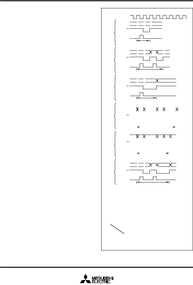
The bus interface unit operates using one of the waveforms (1) to
(6) shown in Figure 5. The standard waveforms are (1) and (2). The ALE signal is used to latch only the address signal from the
multiplexed signal containing data and address.
_
The E signal becomes “L” when the bus interface unit reads an in-
struction code or data from memory or when it writes data to
__
memory. Whether to perform read or write is controlled by the R/W
__
signal. Read is performed when the R/W signal is “H” state and write is performed when it is “L” state.
Waveform (1) in Figure 5 is used to access a single byte or two bytes simultaneously. To read or write two bytes simultaneously, the first address accessed must be even. Furthermore, when accessing an external memory area in memory expansion mode or microprocessor mode, set the bus width selection input pin BYTE to “L”. (external data bus width to 16 bits) The internal memory area is always treated as 16-bit bus width regardless of BYTE.
When performing 16-bit data read or write, if the conditions for simultaneously accessing two bytes are not satisfied, waveform (2) is used to access each byte one by one.
However, when prefetching the instruction code, if the address of the instruction code is odd, waveform (1) is used, and only one
byte is read in the instruction queue buffer.
____
The signals A0 and BHE in Figure 5 are used to control these cases: 1-byte read from even address, 1-byte read from odd address, 2-byte simultaneous read from even and odd addresses, 1-byte write to even address, 1-byte write to odd address, or 2- byte simultaneous write to even and odd addresses. The A0 signal
that is the address bit 0 is “L” when an even number address is
____
accessed. The BHE signal becomes “L” when an odd number address is accessed.
The bit 2 of processor mode register (address 5E16) is the wait bit.
_
When this bit is set to “0”, the “L” width of E signal is 2 times as
long when accessing an external memory area in memory expan-
_
sion mode or microprocessor mode. However, the “L” width of E
signal is not extended when an internal memory area is accessed.
_
When the wait bit is “1”, the “L” width of E signal is not extended
_
for any access. Waveform (3) is an expansion of the “L” width of E
signal in waveform (1). Waveform (4), (5), and (6) are expansion
_
of each “L” width of E signal in waveform (2), first half of waveform (2), and the last half of waveform (2) respectively.
Instruction code read, data read, and data write are described below.
Internal clock φ
Port P2
E
(1)
ALE
Port P2
(2)E
ALE
Port P2
(3)E
ALE
Port P2
(4)E
ALE
Port P2
(5)E
ALE
Port P2
(6)E
ALE
 A
A  D
D
 A
A  D A +1 D
 A
A  D
D
|
|
|
|
|
|
|
|
|
|
|
|
|
|
A |
|
D A +1 |
D |
|
|
||||
|
|
|
|
|
|
|
|
|
|
|
|
|
|
|
|
|
|
|
|
|
|
|
|
|
|
|
|
|
|
|
|
|
|
|
|
|
|
|
|
|
|
|
|
|
|
|
|
|
|
|
|
|
|
|
|
|
|
|
|
|
|
|
|
A |
|
D A +1 D |
|
|
|||||
|
|
|
|
|
|
|
|
|
|
|
|
|
|
|
|
|
|
|
|
|
|
|
|
|
|
|
|
|
|
|
|
|
|
|
|
|
|
|
|
|
|
|
|
|
|
|
|
|
|
|
|
|
|
|
|
|
|
|
|
|
|
|
|
|
|
|
|
|
|
 A
A  D A +1 D
A : Address D : Data
These waveforms are at the memory expansion mode and the microprocessor mode.
|
methodAccess |
Access 2-byte |
Access even |
Access odd |
|
Signal |
simultaneously |
address 1-byte |
address 1-byte |
||
|
|
|
|
|
|
|
A0 |
“L” |
“L” |
“H” |
|
|
|
|
“L” |
“H” |
“L” |
BHE |
|||||
Fig. 5 Relationship between access method and signals A0
____
and BHE
10
MITSUBISHI MICROCOMPUTERS
M37702M2AXXXFP, M37702M2BXXXFP
M37702S1AFP, M37702S1BFP
SINGLE-CHIP 16-BIT CMOS MICROCOMPUTER
Instruction code read will be described first.
The CPU obtains instruction codes from the instruction queue buffer and executes them. The CPU notifies the bus interface unit that it is requesting an instruction code during an instruction code request cycle. If the requested instruction code is not yet stored in the instruction queue buffer, the bus interface unit halts the CPU until it can store more instructions than requested in the instruction queue buffer.
Even if there is no instruction code request from the CPU, the bus interface unit reads instruction codes from memory and stores them in the instruction queue buffer when the instruction queue buffer is empty or when only one instruction code is stored and the bus is idle on the next cycle.
This is referred to as instruction pre-fetching.
Normally, when reading an instruction code from memory, if the accessed address is even the next odd address is read together with the instruction code and stored in the instruction queue buffer. However, in memory expansion mode or microprocessor mode, if the bus width switching pin BYTE is “H”, external data bus width is 8 bits and the address to be read is in external memory area is odd, only one byte is read and stored in the instruction queue buffer. Therefore, waveform (1) or (3) in Figure 5 is used for instruction code read.
Data read and write are described below.
The CPU notifies the bus interface unit when performing data read or write. At this time, the bus interface unit halts the CPU if the bus interface unit is already using the bus or if there is a request with higher priority. When data read or write is enabled, the bus interface unit uses one of the waveforms from (1) to (6) in Figure 5 to perform the operation.
During data read, the CPU waits until the entire data is stored in the data buffer. The bus interface unit sends the address received
from the CPU to the address bus. Then it reads the memory when
_
the E signal is “L” and stores the result in the data buffer.
During data write, the CPU writes the data in the data buffer and the bus interface unit writes it to memory. Therefore, the CPU can proceed to the next step without waiting for write to complete. The
bus interface unit sends the address received from the CPU to the
_
address bus. Then when the E signal is “L”, the bus interface unit sends the data in the data buffer to the data bus and writes it to memory.
11

MITSUBISHI MICROCOMPUTERS
M37702M2AXXXFP, M37702M2BXXXFP M37702S1AFP, M37702S1BFP
SINGLE-CHIP 16-BIT CMOS MICROCOMPUTER
INTERRUPTS
Table 1 shows the interrupt types and the corresponding interrupt
vector addresses. Reset is also treated as a type of interrupt and
____
is discussed in this section, too. DBC is an interrupt used during
debugging.
____
Interrupts other than reset, DBC, watchdog timer, zero divide, and BRK instruction all have interrupt control registers. Table 2 shows the addresses of the interrupt control registers and Figure 6 shows the bit configuration of the interrupt control register.
Use the SEB and CLB instructions when setting each interrupt control register.
The interrupt request bit is automatically cleared by the hardware
during reset or when processing an interrupt.
____
Also, interrupt request bits other than DBC and watchdog timer can be cleared by software.
INT2 to INT0 are external interrupts and whether to cause an interrupt at the input level (level sense) or at the edge (edge sense) can be selected with the level sense/edge sense selection bit. Furthermore, the polarity of the interrupt input can be selected with polarity selection bit.
Timer and UART interrupts are described in the respective section. The priority of interrupts when multiple interrupts are caused simultaneously is partially fixed by hardware, but, it can also be adjusted by software as shown in Figure 7. The hardware priority
is fixed the following:
____
reset > DBC > watchdog timer > other interrupts
Table 1. Interrupt types and the interrupt vector addresses
Interrupts |
Vector addresses |
|
|
|
|
A-D conversion |
00FFD616 |
00FFD716 |
|
|
|
UART1 transmit |
00FFD816 |
00FFD916 |
|
|
|
UART1 receive |
00FFDA16 |
00FFDB16 |
|
|
|
UART0 transmit |
00FFDC16 |
00FFDD16 |
|
|
|
UART0 receive |
00FFDE16 |
00FFDF16 |
Timer B2 |
00FFE016 |
00FFE116 |
Timer B1 |
00FFE216 |
00FFE316 |
Timer B0 |
00FFE416 |
00FFE516 |
Timer A4 |
00FFE616 |
00FFE716 |
Timer A3 |
00FFE816 |
00FFE916 |
Timer A2 |
00FFEA16 |
00FFEB16 |
Timer A1 |
00FFEC16 |
00FFED16 |
|
|
|
Timer A0 |
00FFEE16 |
00FFEF16 |
____ |
|
|
INT2 external interrupt |
00FFF016 |
00FFF116 |
____ |
|
|
INT1 external interrupt |
00FFF216 |
00FFF316 |
____ |
|
|
INT0 external interrupt |
00FFF416 |
00FFF516 |
|
|
|
Watchdog timer |
00FFF616 |
00FFF716 |
____ |
|
|
DBC (unusable) |
00FFF816 |
00FFF916 |
|
|
|
Break instruction |
00FFFA16 |
00FFFB16 |
|
|
|
Zero divide |
00FFFC16 |
00FFFD16 |
|
|
|
Reset |
00FFFE16 |
00FFFF16 |
7 6 5 4 3 2 1 0
Interrupt priority Interrupt request bit
0 : No interrupt
1 : Interrupt
Interrupt control register configuration for A-D converter, UART0, UART1, timer A0 to timer A4, and timer B0 to timer B2
7 6 5 4 3 2 1 0
 Interrupt priority Interrupt request bit
0 : No interrupt
1 : Interrupt Polarity selection bit
0 : Set interrupt request bit at “H” level for level sense and when changing from “H” to “L” level for edge sense.
1 : Set interrupt request bit at “L” level for level sense and when changing from “L” to “H” level for edge sense.
Level sense/edge sense selection bit 0 : Edge sense
1 : Level sense
Interrupt control register configuration for INT2 to INT0.
Fig. 6 Interrupt control register configuration
12
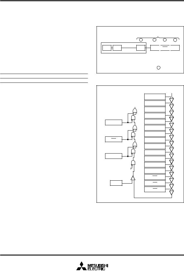
MITSUBISHI MICROCOMPUTERS
M37702M2AXXXFP, M37702M2BXXXFP M37702S1AFP, M37702S1BFP
SINGLE-CHIP 16-BIT CMOS MICROCOMPUTER
Table 2. Addresses of interrupt control registers
Interrupt control registers |
Addresses |
|
|
A-D conversion interrupt control register |
00007016 |
|
|
UART0 transmit interrupt control register |
00007116 |
|
|
UART0 receive interrupt control register |
00007216 |
|
|
UART1 transmit interrupt control register |
00007316 |
|
|
UART1 receive interrupt control register |
00007416 |
|
|
Timer A0 interrupt control register |
00007516 |
|
|
Timer A1 interrupt control register |
00007616 |
|
|
Timer A2 interrupt control register |
00007716 |
|
|
Timer A3 interrupt control register |
00007816 |
Timer A4 interrupt control register |
00007916 |
Timer B0 interrupt control register |
00007A16 |
Timer B1 interrupt control register |
00007B16 |
Timer B2 interrupt control register |
00007C16 |
____ |
|
INT0 interrupt control register |
00007D16 |
____ |
|
INT1 interrupt control register |
00007E16 |
____ |
|
INT2 interrupt control register |
00007F16 |
Interrupts caused by a BRK instruction and when dividing by zero are software interrupts and are not included in this list.
Other interrupts previously mentioned are A-D converter, UART, Timer, INT interrupts. The priority of these interrupts can be changed by changing the priority level in the corresponding interrupt control register by software.
Figure 8 shows a diagram of the interrupt priority resolution circuit. When an interrupt is caused, the each interrupt device compares its own priority with the priority from above and if its own priority is higher, then it sends the priority below and requests the interrupt. If the priorities are the same, the one above has priority.
This comparison is repeated to select the interrupt with the highest priority among the interrupts that are being requested. Finally the selected interrupt is compared with the processor interrupt priority level (IPL) contained in the processor status register (PS) and the request is accepted if it is higher than IPL and the interrupt disable
flag I is “0”. The request is not accepted if flag I is “1”. The reset,
____
DBC, and watchdog timer interrupts are not affected by the interrupt disable flag I.
When an interrupt is accepted, the contents of the processor status register (PS) is saved to the stack and the interrupt disable flag I is set to “1”.
Furthermore, the interrupt request bit of the accepted interrupt is cleared to “0” and the processor interrupt priority level (IPL) in the processor status register (PS) is replaced by the priority level of the accepted interrupt.
Therefore, multi-level priority interrupts are possible by resetting
the interrupt disable flag I to “0” and enable further interrupts.
____
For reset, DBC, watchdog timer, zero divide, and BRK instruction interrupts, which do not have an interrupt control register, the processor interrupt level (IPL) is set as shown in Table 3.
Priority resolution is performed by latching the interrupt request bit and interrupt priority level so that they do not change. They are sampled at the first half and latched at the last half of the operation code fetch cycle.
Because priority resolution takes some time, no sampling pulse is generated for a certain interval even if it is the next operation code fetch cycle.
Priority is determined by hardware
4 |
3 |
2 |
1 |
Watchdog  DBC
DBC  Reset
Reset
timer
A-D converter, UART, Timer, INT interrupts
Priority can be changed with software inside 4
Fig. 7 Interrupt priority
|
Level 0 |
|
A-D conversion |
Interrupt request |
UART1 transmit |
|
UART1 receive |
|
UART0 transmit |
Reset |
UART0 receive |
|
|
|
Timer B2 |
|
Timer B1 |
DBC |
Timer B0 |
|
Timer A4 |
Watchdog |
Timer A3 |
|
|
timer |
Timer A2 |
|
|
|
Timer A1 |
Interrupt disable flag I |
Timer A0 |
|
INT2 |
IPL |
INT1 |
|
INT0 |
Fig. 8 Interrupt priority resolution
13
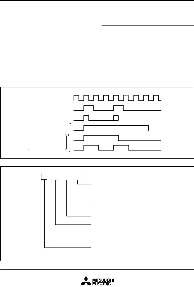
MITSUBISHI MICROCOMPUTERS
M37702M2AXXXFP, M37702M2BXXXFP M37702S1AFP, M37702S1BFP
SINGLE-CHIP 16-BIT CMOS MICROCOMPUTER
As shown in Figure 9, there are three different interrupt priority resolution time from which one is selected by software. After the selected time has elapsed, the highest priority is determined and is processed after the currently executing instruction has been completed.
The time is selected with bits 4 and 5 of the processor mode register (address 5E16) shown in Figure 10. Table 4 shows the relationship between these bits and the number of cycles. After a reset, the processor mode register is initialized to “0016” and therefore, the longest time is selected.
However, the shortest time should be selected by software.
Table 3. Value set in processor interrupt level (IPL) during an interrupt
Interrupt types |
Setting value |
Reset |
0 |
____ |
|
DBC |
7 |
Watchdog timer |
7 |
Zero divide |
Not change value of IPL. |
BRK instruction |
Not change value of IPL. |
Table 4. Relationship between priority level resolution time selection bit and number of cycles
Priority level resolution time selection bit |
Number of cycles |
||
Bit 5 |
Bit 4 |
||
|
|||
0 |
0 |
7 cycles of φ |
|
0 |
1 |
4 cycles of φ |
|
1 |
0 |
2 cycles of φ |
|
φ : internal clock
Internal clock φ
Operation code fetch cycle
Sampling pulse
Priority resolution time
Select from 0 to 2 with bits 4 and 5 of the processor mode register
0
1
2
Fig. 9 Interrupt priority resolution time
7 6 5 4 3 2 1 0
0
Processor mode register (5E 16)
Processor mode bits
0 0 : Single-chip mode
0 1 : Memory expansion mode
1 0 : Microprocessor mode
1 1 : Evaluation chip mode Wait bit
0 : Wait
1 : No wait Software reset bit
The processor is reset when this bit is set to “1”. Priority resolution time selection bits
0 0 : Select 0 in Figure 9
0 1 : Select 1 in Figure 9
1 0 : Select 2 in Figure 9 Test mode bit
Must be “0”
Clock φ1 output selection bit 0 : No φ1 output
1 : φ1 output
Fig. 10 Processor mode register configuration
14
MITSUBISHI MICROCOMPUTERS
M37702M2AXXXFP, M37702M2BXXXFP M37702S1AFP, M37702S1BFP
SINGLE-CHIP 16-BIT CMOS MICROCOMPUTER
TIMER
There are eight 16-bit timers. They are divided by type into timer A
(5) and timer B (3).
The timer I/O pins are shared with I/O pins for port P5 and P6. To use these pins as timer input pins, the data direction register bit corresponding to the pin must be cleared to “0” to specify input mode.
TIMER A
Figure 11 shows a block diagram of timer A.
Timer A has four modes; timer mode, event counter mode, oneshot pulse mode, and pulse width modulation mode. The mode is selected with bits 0 and 1 of the timer Ai mode register (i = 0 to 4). Each of these modes is described below.
(1) Timer mode [00]
Figure 12 shows the bit configuration of the timer Ai mode register during timer mode. Bits 0, 1, and 5 of the timer Ai mode register must always be “0” in timer mode.
Bit 3 is ignored if bit 4 is “0”.
Bits 6 and 7 are used to select the timer counter source.
The counting of the selected clock starts when the count start flag is “1” and stops when it is “0”.
Figure 13 shows the bit configuration of the count start flag. The counter is decremented, an interrupt is caused and the interrupt request bit in the timer Ai interrupt control register is set when the contents becomes 000016. At the same time, the contents of the reload register is transferred to the counter and count is continued.
|
|
|
f2 |
|
f16 |
|
f32 |
|
f64 |
|
f512 |
||||||
|
|
|
|
|
|
|
|
|
|
|
|
|
|
|
|
|
|
f(X IN) |
|
1/2 |
|
|
1/8 |
|
|
1/2 |
|
|
1/2 |
|
|
1/8 |
|
|
|
|
|
|
|
|
|
|
|
|
|
||||||||
|
|
|
|
|
|
|
|
|
|
|
|
|
|
|
|
|
|
Data bus (odd)
Data bus (even) |
|
(Lower 8 bits) |
(Higher 8 bits) |
|
Clock source selection |
• Timer |
Reload register(16) |
|
f2 |
|
|
||
|
• One-shot |
|
|
|
f16 |
|
|
|
|
|
• Pulse width modulation |
|
|
|
f64 |
|
|
|
|
|
|
|
|
|
f512 |
|
Timer (gate function) |
|
|
|
|
Counter(16) |
|
|
|
|
|
Addresses |
|
|
|
|
|
|
|
|
|
|
Event counter |
|
|
|
|
|
Up/Down |
|
Timer A0 4716 |
4616 |
||
|
|
Polarity |
|
|
|
Count start flag |
|
|
Always decremented |
|
Timer A1 |
4916 |
4816 |
|||
TAi IN |
selection |
|
|
|
|
|
|
|
except in event count mode |
|
Timer A2 |
4B16 |
4A16 |
|||
|
|
|
|
|
|
|
|
|
|
|||||||
|
|
|
|
|
(4016) |
|
|
|
|
|||||||
|
|
|
|
|
|
|
|
|
||||||||
(i = 0 – 4) |
|
|
|
|
|
|
|
|
|
Timer A3 |
4D16 |
4C16 |
||||
|
|
|
|
|
|
|
|
|
|
|
||||||
|
|
|
|
|
|
|
|
|
|
|
|
|
|
|||
|
|
|
|
|
External trigger |
|
Down count |
|
|
|
|
|
Timer A4 |
4F16 |
4E16 |
|
|
|
|
|
|
|
|
|
|||||||||
|
|
|
|
|
|
|
|
|
|
|||||||
Up-down flag
(4416)
Pulse output


 Toggle flip-flop TAi OUT
(i = 0 – 4)
Fig. 11 Block diagram of timer A
15
MITSUBISHI MICROCOMPUTERS
M37702M2AXXXFP, M37702M2BXXXFP M37702S1AFP, M37702S1BFP
SINGLE-CHIP 16-BIT CMOS MICROCOMPUTER
When bit 2 of the timer Ai mode register is “1”, the output is generated from TAiOUT pin. The output is toggled each time the contents of the counter reaches to 000016. When the contents of the count start flag is “0”, “L” is output from TAiOUT pin.
When bit 2 is “0”, TAiOUT can be used as a normal port pin. When bit 4 is “0”, TAiIN can be used as a normal port pin. When bit 4 is “1”, counting is performed only while the input signal from the TAiIN pin is “H” or “L” as shown in Figure 14. Therefore, this can be used to measure the pulse width of the TAiIN input signal. Whether to count while the input signal is “H” or while it is “L” is determined by bit 3. If bit 3 is “1”, counting is performed while the TAiIN pin input signal is “H” and if bit 3 is “0”, counting is performed
while it is “L”.
Note that the duration of “H” or “L” on the TAiIN pin must be two or more cycles of the timer count source.
When data is written to timer Ai register with timer Ai halted, the same data is also written to the reload register and the counter. When data is written to timer Ai which is busy, the data is written to the reload register, but not to the counter. The counter is reloaded with new data from the reload register at the next reload timer. The contents of the counter can be read at any time.
When the value set in the timer Ai register is n, the timer frequency dividing ratio is 1/(n + 1).
|
|
|
|
|
|
|
|
|
Addresses |
||
|
|
|
|
|
|
|
|
|
Timer A0 mode register |
5616 |
|
|
|
|
|
|
|
|
|
|
|
||
|
|
|
|
|
|
|
|
|
Timer A1 mode register |
5716 |
|
|
|
|
|
|
|
|
|
|
Timer A2 mode register |
5816 |
|
7 6 5 4 |
3 2 1 |
0 |
|
Timer A3 mode register |
5916 |
|
|||||
|
|
|
|
|
|
|
|
|
Timer A4 mode register |
5A16 |
|
|
|
0 |
|
|
|
0 |
0 |
|
|
||
|
|
|
|
|
|
|
|
|
|||
|
|
|
|
|
|
|
|
|
|
|
|
0 0 : Always “00” in timer mode
0 : No pulse output (TAiOUT is normal port pin) 1 : Pulse output
0 : No gate function (TAiIN is normal port pin) 1 0 : Count only while TAiIN input is “L”
1 1 : Count only while TAiIN input is “H”
0 : Always “0” in timer mode
Clock source selection bit
0 |
0 |
: Select f2 |
0 |
1 |
: Select f16 |
1 |
0 |
: Select f64 |
1 |
1 |
: Select f512 |
Fig. 12 Timer Ai mode register bit configuration during timer mode
16

MITSUBISHI MICROCOMPUTERS
M37702M2AXXXFP, M37702M2BXXXFP
M37702S1AFP, M37702S1BFP
SINGLE-CHIP 16-BIT CMOS MICROCOMPUTER
7 6 5 4 3 2 1 0 |
|
|
|
Count start flag |
Address |
|||||||||||||||
|
|
|
|
|
|
|
|
|
|
|
|
|
|
|
|
|
|
|
(Stop at “0”, Start at “1”) |
4016 |
|
|
|
|
|
|
|
|
|
|
|
|
|
|
|
|
|
|
|
||
|
|
|
|
|
|
|
|
|
|
|
|
|
|
|
|
|
|
|
Timer A0 count start flag |
|
|
|
|
|
|
|
|
|
|
|
|
|
|
|
|
|
|
|
|
|
|
|
|
|
|
|
|
|
|
|
|
|
|
|
|
|
|
|
|
|||
|
|
|
|
|
|
|
|
|
|
|
|
|
|
|
|
|
|
|
Timer A1 count start flag |
|
|
|
|
|
|
|
|
|
|
|
|
|
|
|
|
|
|
|
|||
|
|
|
|
|
|
|
|
|
|
|
|
|
|
|
|
|
|
|
Timer A2 count start flag |
|
|
|
|
|
|
|
|
|
|
|
|
|
|
|
|
|
|
|
|
||
|
|
|
|
|
|
|
|
|
|
|
|
|
|
|
|
|
|
|
Timer A3 count start flag |
|
|
|
|
|
|
|
|
|
|
|
|
|
|
|
|
|
|
|
|
|
|
|
|
|
|
|
|
|
|
|
|
|
|
|
|
|
|
|
|
|
Timer A4 count start flag |
|
|
|
|
|
|
|
|
|
|
|
|
|
|
|
|
|
|
|
|
|
|
|
|
|
|
|
|
|
|
|
|
|
|
|
|
|
|
|
|
|
Timer B0 count start flag |
|
|
|
|
|
|
|
|
|
|
|
|
|
|
|
|
|
|
|
|
|
|
|
|
|
|
|
|
|
|
|
|
|
|
|
|
|
|
|
|
|
Timer B1 count start flag |
|
|
|
|
|
|
|
|
|
|
|
|
|
|
|
|
|
|
|
|
|
|
|
|
|
|
|
|
|
|
|
|
|
|
|
|
|
|
|
|
|
Timer B2 count start flag |
|
|
|
|
|
|
|
|
|
|
|
|
|
|
|
|
|
|
|
|
|
|
Fig. 13 Count start flag bit configuration
Selected clock source f i
TAiN
Timer mode register
Bit 4 |
Bit 3 |
|
|
1 |
0 |
|
|
Timer mode register
Bit 4 |
Bit 3 |
|
|
1 |
1 |
|
|
Fig. 14 Count waveform when gate function is available
17

MITSUBISHI MICROCOMPUTERS
M37702M2AXXXFP, M37702M2BXXXFP M37702S1AFP, M37702S1BFP
SINGLE-CHIP 16-BIT CMOS MICROCOMPUTER
(2) Event counter mode [01]
Figure 15 shows the bit configuration of the timer Ai mode register during event counter mode. In event counter mode, the bit 0 of the timer Ai mode register must be “1” and bit 1 and 5 must be “0”.
The input signal from the TAiIN pin is counted when the count start flag shown in Figure 13 is “1“ and counting is stopped when it is “0”.
Count is performed at the fall of the input signal when bit 3 is “0” and at the rise of the signal when it is “1”.
In event counter mode, whether to increment or decrement the count can be selected with the up-down flag or the input signal from the TAiOUT pin.
When bit 4 of the timer Ai mode register is “0”, the up-down flag is used to determine whether to increment or decrement the count (decrement when the flag is “0” and increment when it is “1”). Figure 16 shows the bit configuration of the up-down flag.
When bit 4 of the timer Ai mode register is “1”, the input signal from the TAiOUT pin is used to determine whether to increment or decrement the count. However, note that bit 2 must be “0” if bit 4 is “1” because if bit 2 is “1”, TAiOUT pin becomes an output pin with pulse output.
The count is decremented when the input signal from the TAiOUT pin is “L” and incremented when it is “H”. Determine the level of the input signal from the TAiOUT pin before valid edge is input to the TAiIN pin.
An interrupt request signal is generated and the interrupt request bit in the timer Ai interrupt control register is set when the counter reaches 000016 (decrement count) or FFFF16 (increment count). At the same time, the contents of the reload register is transferred to the counter and the count is continued.
When bit 2 is “1” and the counter reaches 000016 (decrement count) or FFFF16 (increment count), the waveform reversing polarity is output from TAiOUT pin.
If bit 2 is “0”, TAiOUT pin can be used as a normal port pin. However, if bit 4 is “1“ and the TAiOUT pin is used as an output pin, the output from the pin changes the count direction. Therefore, bit 4 should be “0” unless the output from the TAiOUT pin is to be used to select the count direction.
7 6 5 4 3 2 1 0
|
|
0 |
|
|
|
|
|
|
0 |
1 |
|
|||||
|
|
|
|
|
|
|
|
|
|
|
|
|
|
|
|
|
|
|
|
|
|
|
|
|
|
|
|
|
|
|
|
|
|
|
|
|
|
|
|
|
|
|
|
|
|
|
|
|
|
|
|
|
|
|
|
|
|
|
|
|
|
|
|
|
|
|
|
|
|
|
|
|
|
|
|
|
|
|
|
|
|
|
|
|
|
|
|
|
|
|
|
|
|
|
|
|
|
|
|
|
|
|
|
|
|
|
|
|
|
|
|
|
|
|
|
|
|
|
Addresses
Timer A0 mode register |
5616 |
Timer A1 mode register |
5716 |
Timer A2 mode register |
5816 |
Timer A3 mode register |
5916 |
Timer A4 mode register |
5A16 |
0 1 : Always “01” in event counter mode
0 : No pulse output
1 : Pulse output
0 : Count at the falling edge of input signal
1 : Count at the rising edge of input signal
0 : Increment or decrement according to up-down flag
1 : Increment or decrement according to TAiOUT pin input signal level
0 : Always “0” in event counter mode
: Not used in event counter mode
Fig. 15 Timer Ai mode register bit configuration during event counter mode
7 |
6 |
5 |
4 |
3 |
2 |
1 |
0 |
|
Address |
|
|
|
|
|
|
|
|
Up-down flag |
4416 |
|
|
|
|
|
|
|
|
|
|
Timer A0 up-down flag
Timer A1 up-down flag
 Timer A2 up-down flag
Timer A3 up-down flag
 Timer A4 up-down flag
Timer A2 two-phase pulse signal processing selection bit
0 : Two-phase pulse signal processing disabled
1 : Two-phase pulse signal processing mode
Timer A3 two-phase pulse signal processing selection bit
0 : Two-phase pulse signal processing disabled
1 : Two-phase pulse signal processing mode
Timer A4 two-phase pulse signal processing selection bit
0 : Two-phase pulse signal processing disabled
1 : Two-phase pulse signal processing mode
Fig. 16 Up-down flag bit configuration
18
Loading...