


MITSUBISHI MICROCOMPUTERS
7630 Group
SINGLE-CHIP 8-BIT CMOS MICROCOMPUTER
DESCRIPTION
The 7630 group is a single chip 8-bit microcomputer designed with CMOS silicon gate technology.
Being equipped with a CAN (Controller Area Network) module circuit, the microcomputer is suited to drive automotive equipments. The CAN module complies with CAN specification version 2.0, part B and allows priority-based message management.
In addition to the microcomputers simple instruction set, the ROM, RAM and I/O addresses are placed in the same memory map to enable easy programming.
The built-in ROM is available as mask ROM or One Time PROM. For development purposes, emulatorand EPROM-type microcomputers are available as well.
FEATURES
z Basic machine-language instructions . . . . . . . . . . . . . . . . . . 71
zMinimum instruction execution time
(at 10 MHz oscillation frequency) . . . . . . . . . . . . . . . . . . 0.2 μs
zMemory size
ROM . . . . . . . . . . . . . . . . .16252 bytes (M37630M4T-XXXFP) RAM . . . . . . . . . . . . . . . . . . .512 bytes (M37630M4T-XXXFP)
zI/O ports
Programmable I/O ports . . . . . . . . . . . . . . . . . . . . . . . . . . . . 35
Input . . . . . . . . . . . . . . . . . . . . . . . . . . . . . . . . . . . . . . . . . . . . 1
z Interrupts . . . . . . . . . . . . . . . . . . . . . . . . 24 sources, 24 vectors
zTimers
16-bit Timers . . . . . . . . . . . . . . . . . . . . . . . . . . . . . . 2 channels 8-bit Timers . . . . . . . . . . . . . . . . . . . . . . . . . . . . . . . 3 channels
zSerial I/Os
Clock synchronous. . . . . . . . . . . . . . . . . . . . . . . . . . . 1 channel UART . . . . . . . . . . . . . . . . . . . . . . . . . . . . . . . . . . . . . 1 channel
zCAN module
(CAN specification version 2.0, part B) . . . . . . . . . . . 1 channel z A-D converter . . . . . . . . . . . . . . . . . . . . . . . . 8-bits x 8 channels z Watchdog timer . . . . . . . . . . . . . . . . . . . . . . . . . . . . . . . . . . . . 1 z Clock Generating Circuit . . . . . . . . . . . . . . . . . . . . . . . . . . . . . 1
Built-in with internal feedback resistor
zPower source voltage
(at 10 MHz oscillation frequency). . . . . . . . . . . . . . . 4.0 to 5.5 V
zPower dissipation
In high-speed mode . . . . . . . . . . . . . . . . . . . . . . . . . . . . 55 mW (at 8 MHz oscillation frequency, at 5 V power source voltage)
z Operating temperature range. . . . . . . . . . . . . . . . . –40 to 85 °C z Package . . . . . . . . . . . . . . . . . . . . . . . . . . . . 44QFP (44P6N-A)
APPLICATION
Automotive controls
PIN CONFIGURATION (TOP VIEW)
|
|
|
|
|
|
|
|
|
|
|
|
|
|
/PWM |
1 |
0 |
|
/TX |
/INT |
|
/INT |
|
/AN |
|
/AN |
|
/AN |
|
/AN |
|
/AN |
|
|
|
|
|
|
|
||||||||||||||
|
|
|
|
|
|
|
|
|
|
|
|
|
|
|
/CNTR |
|
/CNTR |
|
|
|
|
|
|
|
|
|
|
|
|
|
||||||||||||||||||||||
|
|
|
|
|
|
|
|
|
|
|
|
|
|
|
|
|
|
|
|
|
0 |
|
1 |
0 |
7 |
6 |
5 |
4 |
3 |
|
|
|
|
|
|
|
|
|
|
|||||||||||||
|
|
|
|
|
|
|
|
|
|
|
6 |
5 |
4 |
|
3 |
|
2 |
1 |
7 |
6 |
5 |
4 |
3 |
|
|
|
|
|
|
|
|
|
|
|||||||||||||||||||
|
|
|
|
|
|
|
|
|
|
|
|
|
|
P1 |
|
P1 |
|
P1 |
P1 |
P1 |
|
P1 |
|
P0 |
|
P0 |
|
P0 |
|
P0 |
|
P0 |
|
|
|
|
|
|
|
|||||||||||||
|
|
|
|
|
|
|
|
|
|
|
|
|
|
|
|
|
|
|
|
|
|
|
|
|
|
|
|
|
|
|
|
|
|
|
|
|
|
|
|
|
|
|
|
|
|
|
|
|
|
|
||
|
|
|
|
|
|
|
|
|
|
|
|
|
|
|
|
|
|
|
|
|
|
|
|
|
|
|
|
|
|
|
|
|
|
|
|
|
|
|
|
|
|
|
|
|
|
|
|
|
|
|
|
|
|
|
|
|
|
|
|
|
|
|
|
|
|
|
|
|
|
|
|
|
|
|
|
|
|
|
|
|
|
|
|
|
|
|
|
|
|
|
|
|
|
|
|
|
|
|
|
|
|
|
|
|
|
|
|
|
|
|
|
|
|
|
|
|
|
|
|
|
|
|
|
|
|
|
|
|
|
|
|
|
|
|
|
|
|
|
|
|
|
|
|
|
|
|
|
|
|
|
|
|
|
|
|
|
|
|
|
|
|
|
|
|
|
|
|
|
|
|
|
|
33 |
|
32 |
|
31 |
|
30 |
|
29 |
|
28 |
|
27 |
|
26 |
|
25 |
|
24 |
|
23 |
|
|
|
|
|
|
|
|
|
|
||||||||
|
|
|
P17 |
|
|
|
|
|
|
|
|
|
|
|
|
|
|
|
|
|
|
|
|
|
|
|
|
|
|
|
|
|
|
|
|
|
|
|
|
|
|
|
|
|
|
|
P02/AN2 |
|||||
|
|
|
|
|
|
|
|
|
|
|
|
|
|
|
|
|
|
|
|
|
|
|
|
|
|
|
|
|
|
|
|
|
|
|
|
|
|
|
|
|
|
|
|
|
|
|||||||
|
|
|
|
|
|
|
|
|
|
|
|
|
|
|
|
|
|
|
|
|
|
|
|
|
|
|
|
|
|
|
|
|
|
|
|
|
|
|
|
|
|
|
|
|
|
|||||||
|
|
|
|
|
|
34 |
|
|
|
|
|
|
|
|
|
|
|
|
|
|
|
|
|
|
|
|
|
|
|
|
|
|
|
|
|
|
|
|
|
22 |
|
|
|
|
|
|||||||
P20/SIN |
|
|
|
|
|
|
|
|
|
|
|
|
|
|
|
|
|
|
|
|
|
|
|
|
|
|
|
|
|
|
|
|
|
|
|
|
|
|
|
|
|
|
|
P01/AN1 |
||||||||
|
|
|
35 |
|
|
|
|
|
|
|
|
|
|
|
|
|
|
|
|
|
|
|
|
|
|
|
|
|
|
|
|
|
|
|
|
|
21 |
|
|
|
|
|
||||||||||
P21/SOUT |
|
|
|
|
|
|
|
|
|
|
|
|
|
|
|
|
|
|
|
|
|
|
|
|
|
|
|
|
|
|
|
|
|
|
|
|
|
|
|
|
|
|
|
P00/AN0 |
||||||||
|
|
|
36 |
|
|
|
|
|
|
|
|
|
|
|
|
|
|
|
|
|
|
|
|
|
|
|
|
|
|
|
|
|
|
|
|
|
20 |
|
|
|
|
|
||||||||||
P22/SCLK |
|
|
|
|
|
|
|
|
|
|
|
|
|
|
|
|
|
|
|
|
|
|
|
|
|
|
|
|
|
|
|
|
|
|
|
|
|
|
|
|
|
|
|
VREF |
||||||||
|
|
|
37 |
|
|
|
M37630M4T-XXXFP |
|
|
|
|
|
19 |
|
|
|
|
|
||||||||||||||||||||||||||||||||||
|
|
|
|
|
|
|
|
|
|
|
|
|
|
|
|
|
|
|
|
|
|
|
|
|
|
AVSS |
||||||||||||||||||||||||||
P23/SRDY |
|
|
|
|
38 |
|
|
|
|
|
|
|
|
18 |
|
|
|
|
|
|||||||||||||||||||||||||||||||||
|
|
|
VSS |
|
|
|
|
|
|
|
|
|
|
|
|
|
|
|
|
|
|
|
|
|
|
|
|
|
|
|
|
|
|
|
|
|
|
|
|
|
|
|
|
VCC |
||||||||
|
|
|
39 |
|
|
|
M37630E4T-XXXFP |
|
|
|
|
17 |
||||||||||||||||||||||||||||||||||||||||
|
|
|
|
|
|
|
|
|
|
|
|
|
|
|
XOUT |
|||||||||||||||||||||||||||||||||||||
P24/URXD |
|
|
40 |
|
|
|
|
|
|
|
|
|
|
|
|
|
|
|
|
|
|
|
|
|
|
|
|
|
|
|
|
|
|
|
|
|
16 |
|
|
|
|
|
||||||||||
P25/UTXD |
|
|
|
|
|
|
|
|
|
|
|
|
|
|
|
|
|
|
|
|
|
|
|
|
|
|
|
|
|
|
|
|
|
|
|
|
|
|
|
|
|
|
XIN |
|||||||||
|
41 |
|
|
|
|
|
|
|
|
|
|
|
|
|
|
|
|
|
|
|
|
|
|
|
|
|
|
|
|
|
|
|
|
|
15 |
|
|
|
|
|
||||||||||||
P26 |
|
|
|
|
|
|
|
|
|
|
|
|
|
|
|
|
|
|
|
|
|
|
|
|
|
|
|
|
|
|
|
|
|
|
|
|
|
|
|
|
|
|
|
|
|
|
|
|
|
|
VSS |
|
/URTS |
|
|
|
|
42 |
|
|
|
|
|
|
|
|
|
|
|
|
|
|
|
|
|
|
|
|
|
|
|
|
|
|
|
|
|
|
|
|
|
14 |
|
|
|
|
|
||||||||
|
|
|
|
|
|
|
|
|
|
|
|
|
|
|
|
|
|
|
|
|
|
|
|
|
|
|
|
|
|
|
|
|
|
|
|
|
|
|
|
|
|
|
|
|
|
|
|
|
|
|
|
|
P27/UCTS |
|
|
|
43 |
|
|
|
|
|
|
|
|
|
|
|
|
|
|
|
|
|
|
|
|
|
|
|
|
|
|
|
|
|
|
|
|
|
13 |
|
|
|
|
|
RESET |
||||||||
|
|
|
P30 |
|
|
|
|
|
|
|
|
|
|
|
|
|
|
|
|
|
|
|
|
|
|
|
|
|
|
|
|
|
|
|
|
|
|
|
|
|
|
|
|
|
|
|
P47/KW7 |
|||||
|
|
|
|
|
44 |
|
|
|
|
|
|
|
|
|
|
|
|
|
|
|
|
|
|
|
|
|
|
|
|
|
|
|
|
|
|
|
|
|
12 |
|
|
|
|
|
||||||||
|
|
|
|
|
|
|
|
|
|
|
|
|
|
|
|
|
|
|
|
|
|
|
|
|
|
|
|
|
|
|
|
|
|
|
|
|
|
|
|
|
|
|
|
|
|
|
|
|
|
|
|
|
|
|
|
|
|
|
|
|
|
|
|
|
|
|
|
|
|
|
|
|
|
|
|
|
|
|
|
|
|
|
|
|
|
|
|
|
|
|
|
|
|
|
|
|
|
|
|
|
|
|
|
|
|
|
|
|
|
|
|
|
|
|
|
|
|
|
|
1 |
|
2 |
|
3 |
|
4 |
|
5 |
|
6 |
|
7 |
|
8 |
|
9 |
|
10 |
|
11 |
|
|
|
|
|
|
|
|
|
|
||||||||
|
|
|
|
|
|
|
|
|
|
|
|
|
|
|
|
|
|
|
|
|
|
|
|
|
|
|
|
|
|
|
|
|
|
|
|
|
|
|
|
|
|
|
|
|
|
|
|
|
|
|
|
|
|
|
|
|
|
|
|
|
|
|
|
|
|
|
|
|
|
|
|
|
|
|
|
|
|
|
|
|
|
|
|
|
|
|
|
|
|
|
|
|
|||||||||||||
|
|
|
|
|
|
|
|
|
|
|
|
|
|
|
|
|
|
|
|
|
|
|
|
|
|
|
|
|
|
|
|
|
|
|
|
|
|
|
|
|
|
|
|
|
|
|
||||||
|
|
|
|
|
|
|
|
|
|
|
|
|
|
/CTX |
|
/CRX |
3 |
|
4 |
|
0 |
1 |
2 |
3 |
4 |
5 |
6 |
|
|
|
|
|
|
|
|
|
|
|||||||||||||||
|
|
|
|
|
|
|
|
|
|
|
|
|
|
|
|
P3 |
P3 |
/KW |
|
/KW |
|
/KW |
|
/KW |
|
/KW |
|
/KW |
|
/KW |
|
|
|
|
|
|
|
|||||||||||||||
|
|
|
|
|
|
|
|
|
|
|
1 |
2 |
|
|
|
|
|
|
|
0 |
1 |
2 |
3 |
4 |
5 |
6 |
|
|
|
|
|
|
|
|
|
|
||||||||||||||||
|
|
|
|
|
|
|
|
|
|
|
|
|
|
P3 |
|
P3 |
|
|
|
|
|
|
|
P4 |
|
P4 |
|
P4 |
|
P4 |
|
P4 |
|
P4 |
|
P4 |
|
|
|
|
|
|
|
|||||||||
Package type: 44P6N-A 44-pin plastic molded QFP
Fig. 1 Pin configuration of M37630M4T–XXXFP
MITSUBISHI |
1 |
ELECTRIC |
2 |
Fig |
|
|
|
|
|
|
|
|
|
|
|
|
|
|
|
|
|
|
|
|
|
2 . |
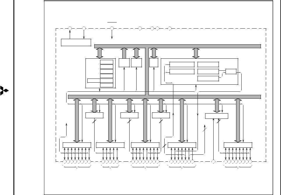
M37630MXT-XXXFP FUNCTIONAL BLOCK DIAGRAM (PACKAGE: 44P6N-A) |
|
|
|
||||||||||||||||
|
blockFunctional |
|
|
|
|||||||||||||||||
|
Clock |
|
|
Clock |
|
|
Reset |
|
|
|
|
|
|
|
|
|
|
||||
|
|
|
|
|
|
|
|
|
|
|
|
|
|
|
|
||||||
|
|
output |
|
|
input |
|
|
input |
|
VCC |
|
VSS |
AVSS |
|
|
|
|
|
|||
|
|
XOUT |
|
|
XIN |
|
|
RESET |
|
|
|
|
|
|
|||||||
|
|
16 |
|
|
15 |
|
|
|
|
13 |
|
|
17 |
14 |
39 |
18 |
|
|
|
|
|
|
diagram |
Clock generating circuit |
|
|
|
|
|
|
|
|
|
|
|
|
|
|
|||||
|
|
|
|
|
|
|
|
|
|
|
|
|
|
|
|
||||||
|
|
|
|
|
|
|
CPU |
A (8) |
|
|
ROM |
RAM |
WDT |
Timer X (16) |
Timer 1 (8) |
|
|
|
|
||
|
|
|
|
|
|
|
|
X (8) |
|
|
|
|
|
|
|
|
|
|
|||
|
|
|
|
|
|
|
|
|
|
|
|
|
|
2 |
|
|
|
|
|
||
|
|
|
|
|
|
|
|
Y (8) |
|
|
|
|
|
|
Timer Y (16) |
Timer 2 (8) |
PWM |
|
|
|
|
|
|
|
|
|
|
|
|
S (8) |
|
|
|
|
|
|
|
Timer 3 (8) |
|
|
|
|
|
|
|
|
|
|
|
|
PCH (8) |
PCL (8) |
|
|
|
|
|
|
|
|
|
|
|||
|
|
|
|
|
|
|
|
|
|
|
|
|
|
|
|
|
|
||||
|
|
|
|
|
|
|
|
PS (8) |
|
|
|
|
|
|
|
|
|
|
|
||
MITSUBISHI ELECTRIC |
|
key on |
|
|
|
|
CAN |
|
|
|
|
UART |
|
Serial I/O |
A-D Converter |
|
|
|
|||
|
|
|
|
|
|
|
|
|
|
|
|
|
|
||||||||
|
|
wake up |
|
|
|
|
2 |
|
|
|
|
4 |
|
|
|
4 |
INT0, INT1 |
8 |
MICROCOMPUTERCMOSBIT-8CHIP-SINGLE |
Group7630 |
MICROCOMPUTERSMITSUBISHI |
|
|
|
|
|
|
|
|
|
|
|
|
|
|
||||||||
|
|
|
|
|
|
|
|
|
|
|
|
|
|
|
|
|
|||||
|
|
|
|
|
|
|
|
|
|
|
|
|
|
|
|
|
2 |
|
|
|
|
|
|
P4 (8) |
|
|
|
P3 (5) |
|
P2 (8) |
|
|
P1 (7) |
|
P0 (8) |
|
|
|
|||||
|
|
|
|
|
|
|
|
|
|
|
|
|
|
|
|
3 |
|
|
|
|
|
|
|
12 11 10 |
9 |
8 |
7 |
6 |
5 |
4 |
3 |
2 |
1 |
44 |
43 42 41 40 38 37 36 35 |
34 33 32 31 30 29 28 |
19 |
27 26 25 24 23 22 21 20 |
|
|
|
||
|
|
|
|
|
|
|
|
|
|
|
|
|
|
|
|
|
VREF input |
|
|
|
|
|
|
I/O port P4 |
|
|
|
I/O port P3 |
I/O port P2 |
|
I/O port P1 |
|
I/O port P0 |
|
|
|
|||||||

MITSUBISHI MICROCOMPUTERS
7630 Group
SINGLE-CHIP 8-BIT CMOS MICROCOMPUTER
PIN DESCRIPTION
Table 1: Pin description
|
|
Pin |
Name |
Input/Output |
Description |
|||
|
|
|
|
|
|
|
|
|
|
VCC, VSS |
Power source |
|
Power supply pins; apply 4.0 to 5.5 V to VCC and 0 V to VSS |
||||
|
voltage |
|
||||||
|
|
|
|
|
|
|
|
|
|
|
|
|
|
|
|
|
|
|
AVSS |
Analog power |
|
Ground pin for A-D converter. Connect to VSS |
||||
|
source voltage |
|
||||||
|
|
|
|
|
|
|
|
|
|
|
|
|
|
|
|
|
|
|
|
|
|
|
|
|
|
Reset pin. This pin must be kept at “L” level for more than 2 μs, to enter the reset |
|
|
|
|
|
|
Reset input |
Input |
state. If the crystal or ceramic resonator requires more time to stabilize, extend the |
|
RESET |
|||||||
|
|
|
|
|
|
|
|
“L” level period. |
|
|
|
|
|
|
|
|
|
|
XIN |
Clock input |
Input |
Input and output pins of the internal clock generating circuit. Connect a ceramic or |
||||
|
|
|
|
|
|
|
|
quartz–crystal resonator between the XIN and XOUT pins. When an external clock |
|
XOUT |
Clock output |
Output |
|||||
|
source is used, connect it to XIN and leave XOUT open. |
|||||||
|
VREF |
Reference volt- |
Input |
Reference voltage input pin for A-D converter |
||||
|
age input |
|||||||
|
|
|
|
|
|
|
|
|
|
|
|
|
|
|
|
|
|
|
P00/AN0— |
I/O port P0 |
I/O |
CMOS I/O ports or analog input ports |
||||
|
P07/AN7 |
|||||||
|
|
|
|
|||||
|
|
|
|
|
|
|
|
|
|
|
|
|
|
|
|
|
CMOS input port or external interrupt input port. The active edge (rising or falling) of |
|
P11/INT0 |
|
Input |
external interrupts can be selected. This pin will be used as VPP pin during PROM |
||||
|
|
|
|
|
|
|
|
programming of One Time PROM Versions. |
|
|
|
|
|
|
|
|
|
|
P12/INT1 |
|
|
CMOS I/O port or external interrupt input port. The active edge (rising or falling) of |
||||
|
|
|
external interrupts can be selected. |
|||||
|
|
|
|
|
|
|
|
|
|
|
|
|
|
|
|
|
|
|
P13/TX0 |
|
|
CMOS I/O port or input pin used in the bi-phase counter mode |
||||
|
|
|
|
|
|
|
|
|
|
P14/CNTR0 |
I/O port P1 |
I/O |
CMOS I/O port or timer X input pin used for the event counter, pulse width measure- |
||||
|
ment and bi-phase counter mode |
|||||||
|
|
|
|
|
|
|
|
|
|
|
|
|
|
|
|
|
|
|
P15/CNTR1 |
|
|
CMOS I/O port or timer Y input pin used for the event counter, pulse width and pulse |
||||
|
|
|
period measurement mode |
|||||
|
|
|
|
|
|
|
|
|
|
|
|
|
|
|
|
|
|
|
P16/PWM |
|
|
CMOS I/O port or PWM output pin used in the PWM mode of timers 2 and 3 |
||||
|
|
|
|
|
|
|
|
|
|
P17 |
|
|
CMOS I/O port |
||||
|
|
|
|
|
|
|
|
|
|
P20/SIN |
|
|
|
||||
|
P21/SOUT |
|
|
CMOS I/O ports or clock synchronous serial I/O pins |
||||
|
P22/SCLK |
|
|
|||||
|
|
|
|
|||||
|
|
|
|
|
|
|
|
|
|
P23/SRDY |
|
I/O |
|
||||
|
|
|
|
|
|
I/O port P2 |
|
|
|
P24/URXD |
|
||||||
|
|
|
|
|||||
|
P25/UTXD |
|
|
CMOS I/O ports or asynchronous serial I/O pins |
||||
|
|
|
|
|
|
|
|
|
|
P26/URTS |
|
|
|||||
|
|
|
|
|||||
|
|
|
|
|
|
|
||
|
P27/UCTS |
|
|
|
||||
|
P30 |
|
|
CMOS I/O port |
||||
|
|
|
|
|
|
|
|
|
|
P31/CTX |
I/O port P3 |
I/O |
CMOS I/O port or CAN transmit data pin |
||||
|
|
|
|
|
|
|
||
|
P32/CRX |
CMOS I/O port or CAN receive data pin |
||||||
|
|
|
||||||
|
|
|
|
|
|
|
|
|
|
P33—P3 4 |
|
|
CMOS I/O port |
||||
|
|
|
|
|
|
|
|
|
|
P40/KW0— |
I/O port P4 |
I/O |
CMOS I/O ports. These ports can be used for key-on wake-up when configured as |
||||
|
P47/KW7 |
inputs. |
||||||
|
|
|
||||||
|
|
|
|
|
|
|
|
|
|
|
|
|
|
|
|
|
|
MITSUBISHI |
|
ELECTRIC |
3 |

MITSUBISHI MICROCOMPUTERS
7630 Group
SINGLE-CHIP 8-BIT CMOS MICROCOMPUTER
PART NUMBERING
Product |
M37630 M 4 T– XXX FP |
||
|
|
|
|
Package type
FP: 44P6N-A package
FS: 80D0 package
ROM number
Omitted in One Time PROM version (blank) and EPROM version
T: Automotive use
ROM/PROM size 4: 16384 bytes
The first 128 bytes and the last 4 bytes of ROM are reserved areas.
They cannot be used.
Memory type
M: Mask ROM version
E: EPROM or One Time PROM version
Fig. 3 Part numbering
4 |
MITSUBISHI |
|
ELECTRIC |
||
|
MITSUBISHI MICROCOMPUTERS
7630 Group
SINGLE-CHIP 8-BIT CMOS MICROCOMPUTER
GROUP EXPANSION
Mitsubishi plans to expand the 7630 group as follows: |
Memory Size |
|
|
|||
|
|
|
ROM/PROM size . . . . . . . . . . . . . . . . . . . . . . . . . . . . . 16 Kbytes |
|||
Memory Type |
|
|
RAM size. . . . . . . . . . . . . . . . . . . . . . . . . . . . . . . . . . . . 512 bytes |
|||
|
|
Package |
|
|
|
|
|
|
|
|
|
|
|
Support mask ROM, One Time PROM and EPROM versions. |
44P6N-A |
. . . . . . . . . . . . . . . . .0.8mm-pitch plastic molded QFP |
||||
|
|
|
||||
|
|
|
80D0 . . . . . . . . . . .0.8mm-pitch ceramic LCC (EPROM version) |
|||
ROM |
|
|
|
|
|
|
External |
|
|
|
|
|
|
60K |
|
|
|
|
|
|
48K |
|
|
|
|
|
|
32K |
|
|
|
|
|
|
28K |
|
|
|
|
|
|
24K |
|
|
|
|
|
|
20K |
|
|
Under development |
|
|
|
|
|
|
|
|
||
|
|
M37630M4T |
|
|
|
|
16K |
|
M37630E4T |
|
|
|
|
|
|
|
|
|
|
|
12K |
Mass product |
|
|
|
|
|
8K |
|
|
|
|
|
|
|
384 |
512 |
640 |
768 |
896 |
1024 |
|
|
|
RAM size (bytes) |
|
|
|
Fig. 4 Memory expansion plan
Currently supported products are listed below:
Table 2: List of supported products |
|
|
As of March 1998 |
||
|
|
|
|
|
|
Product |
(P)ROM size (bytes) |
RAM size (bytes) |
Package |
Remarks |
|
ROM size for User ( ) |
|||||
|
|
|
|
||
|
|
|
|
|
|
M37630M4T-XXXFP |
|
|
|
Mask ROM version |
|
|
|
|
|
|
|
M37630E4T-XXXFP |
16384 |
512 |
44P6N-A |
One Time PROM version |
|
|
|
|
|
|
|
M37630E4FP |
(16252) |
|
|
One Time PROM version (blank) |
|
|
|
|
|
|
|
M37630E4FS |
|
|
80D0 |
EPROM version |
|
|
|
|
|
|
|
MITSUBISHI |
|
ELECTRIC |
5 |

MITSUBISHI MICROCOMPUTERS
7630 Group
SINGLE-CHIP 8-BIT CMOS MICROCOMPUTER
FUNCTIONAL DESCRIPTION
Central Processing Unit (CPU)
The core of 7630 group microcomputers is the 7600 series CPU. This core is based on the standard instruction set of 740 series; however the performance is improved by allowing to execute the same instructions as that of the 740 series in less cycles. Refer to the 7600 Series Software Manual for details of the instruction set.
CPU Mode Register CPUM
The CPU mode register contains the stack page selection bit and internal system clock selection bit. The CPU mode register is allocated to address 000016.
7 |
0 |
|
|
CPU mode register (address 000016) |
|||||||||||||||||||
|
|
|
|
|
|
|
|
|
|
|
|
|
|
|
|
|
|
|
|
||||
|
|
|
|
|
|
|
|
|
|
|
|
|
|
|
|
|
|
||||||
|
|
|
|
|
|
|
|
|
|
|
|
|
|
|
|
|
|
|
|
CPUM |
|
|
|
|
|
|
|
|
|
|
|
|
|
|
|
|
|
|
|
|
|
|
|
||||
|
|
|
|
|
|
|
|
|
|
|
|
|
|
|
|
|
|
|
|
Processor mode bits (set these bits to “00”) |
|||
|
|
|
|
|
|
|
|
|
|
|
|
|
|
|
|
|
|
|
|
||||
|
|
|
|
|
|
|
|
|
|
|
|
|
|
|
|
|
|
|
|
b1 b0 |
|
||
|
|
|
|
|
|
|
|
|
|
|
|
0 |
0: |
Single–chip mode |
|||||||||
|
|
|
|
|
|
|
|
|
|
|
|
0 |
1: |
Not used |
|||||||||
|
|
|
|
|
|
|
|
|
|
|
|
1 |
0: |
Not used |
|||||||||
|
|
|
|
|
|
|
|
|
|
|
|
1 |
1: |
Not used |
|||||||||
|
|
|
|
|
|
|
|
|
|
|
|
|
|
|
|
|
|
|
|
Stack page selection bit |
|||
|
|
|
|
|
|
|
|
|
|
|
|
|
|
|
|
|
|
|
|||||
|
|
|
|
|
|
|
|
|
|
|
|
|
|
|
|
|
|
|
|
|
0 |
: |
0 page |
|
|
|
|
|
|
|
|
|
|
|
|
|
|
|
|
|
|
|
|
|
1 |
: |
1 page |
|
|
|
|
|
|
|
|
|
|
|
|
|
|
|
|
|
|
|
|
Not used (“0” when read, do not write “1”) |
|||
|
|
|
|
|
|
|
|
|
|
|
|
|
|
|
|
|
|
|
|
||||
|
|
|
|
|
|
|
|
|
|
|
|
|
|
|
|
|
|
|
|
Internal system clock selection bit |
|||
|
|
|
|
|
|
|
|
|
|
|
|
|
|
|
|
|
|
|
|
||||
|
|
|
|
|
|
|
|
|
|
|
|
|
|
|
|
|
|
|
|
|
0 |
: |
φ=f(XIN) divided by 2 (high–speed mode) |
|
|
|
|
|
|
|
|
|
|
|
|
|
|
|
|
|
|
|
|
|
1 |
: |
φ=f(XIN) divided by 8 (middle–speed mode) |
|
|
|
|
|
|
|
|
|
|
|
|
|
|
|
|
|
|
|
|
Not used (“0” when read, do not write “1”) |
|||
|
|
|
|
|
|
|
|
|
|
|
|
|
|
|
|
|
|
|
|
||||
|
|
|
|
|
|||||||||||||||||||
Fig. 5 |
Structure of CPU mode register |
|
|
|
|||||||||||||||||||
6 |
MITSUBISHI |
|
ELECTRIC |
||
|
MITSUBISHI MICROCOMPUTERS
7630 Group
SINGLE-CHIP 8-BIT CMOS MICROCOMPUTER
MEMORY
Special Function Register (SFR) Area |
Interrupt Vector Area |
The special function register (SFR) area contains the registers relating to functions such as I/O ports and timers.
The interrupt vector area is for storing jump destination addresses used at reset or when an interrupt is generated.
RAM
RAM is used for data storage and for stack area of subroutine calls and interrupts.
Zero Page
This area can be accessed most efficiently by means of the zero page addressing mode.
ROM
ROM is used for storing user’s program code as well as the interrupt vector area.
Special Page
This area can be accessed most efficiently by means of the special page addressing mode.
RAM area |
|
|
|
|
|
|
|
|
|
|
|
|
|
|
|
|
|
|
|
RAM size |
|
Address |
|
|
|
|
000016 |
||
(byte) |
|
XXXX16 |
|
|
|
|
|||
|
|
|
|
|
|
|
|||
|
|
|
|
|
|
|
|
|
|
192 |
|
011F16 |
|
|
|
|
004016 |
||
|
|
|
|
|
|
|
|
||
256 |
|
015F16 |
|
|
|
|
|
|
|
|
|
|
|
|
|
|
|
|
|
384 |
|
01DF16 |
|
|
|
|
|
006016 |
|
|
|
|
|
|
|
||||
|
|
|
|
|
|
|
|
|
00FF16 |
512 |
|
025F16 |
|
|
|
|
|
||
|
|
|
|
|
|
|
|
|
|
640 |
|
02DF16 |
|
User RAM |
|
|
|||
|
|
|
|
||||||
|
|
|
|
|
|
|
|||
768 |
|
035F16 |
|
|
|
|
|
|
|
|
|
|
|
|
|
|
|
|
|
896 |
|
03DF16 |
|
|
|
|
|
XXXX16 |
|
|
|
|
|
|
|
|
|
|
|
1024 |
|
045F16 |
|
|
|
|
|||
|
|
|
|
|
|
||||
|
|
|
|
|
|
|
|||
|
|
|
|
|
|
|
|
|
|
1536 |
|
06DF16 |
|
|
|
|
|
|
|
|
|
|
|
|
|
|
|
086016 |
|
2048 |
|
085F16 |
|
|
|
|
|||
|
|
|
|
|
|
|
|
|
|
ROM area |
|
|
|
|
|
|
|
|
|
|
|
|
|
|
|
|
|
|
|
ROM size |
|
Address |
|
Address |
|
|
|
|
|
(byte) |
|
YYYY16 |
|
ZZZZ16 |
|
|
|
|
|
|
|
|
|
|
|
|
|
|
|
4096 |
|
F00016 |
|
F08016 |
|
|
|
|
YYYY16 |
|
|
|
|
|
|
|
|
|
|
8192 |
|
E00016 |
|
E08016 |
|
|
|
|
ZZZZ16 |
|
|
|
|
|
|
|
|
|
|
12288 |
|
D00016 |
|
D08016 |
|
|
|
|
|
|
|
|
|
|
|
|
|||
|
|
|
|
|
|
|
|
|
|
16384 |
|
C00016 |
|
C08016 |
|
|
|
|
|
|
|
|
|
|
|
|
|
|
|
20480 |
|
B00016 |
|
B08016 |
|
|
|
|
|
|
|
|
|
|
|
|
|
|
|
24576 |
|
A00016 |
|
A08016 |
|
|
|
|
|
|
|
|
|
|
|
ROM |
|
|
|
28672 |
|
900016 |
|
908016 |
|
|
|
FF0016 |
|
|
|
|
|
|
|
|
|
|
|
32768 |
|
800016 |
|
808016 |
|
|
|
|
|
|
|
|
|
|
|
|
|||
|
|
|
|
|
|
|
|
|
|
36864 |
|
700016 |
|
708016 |
|
|
|
|
FFCA16 |
|
|
|
|
|
|
|
|
|
|
40960 |
|
600016 |
|
608016 |
|
|
|
|
FFFB16 |
|
|
|
|
|
|
|
|
|
|
45056 |
|
500016 |
|
508016 |
|
|
|
|
FFFC16 |
|
|
|
|
|
|
FFFF16 |
|||
|
|
|
|
|
|
|
|
|
|
49152 |
|
400016 |
|
408016 |
|
|
|
||
|
|
|
|
|
|
|
|||
|
|
|
|
|
|
|
|
|
|
53248 |
|
300016 |
|
308016 |
|
|
|
|
|
|
|
|
|
|
|
|
|
|
|
57344 |
|
200016 |
|
208016 |
|
|
|
|
|
|
|
|
|
|
|
|
|
|
|
61440 |
|
100016 |
|
108016 |
|
|
|
|
|
|
|
|
|
|
|
|
|
|
|
SFR area
Not used
Reserved ROM area
Interrupt vector area
Reserved ROM area
CAN |
Zero page |
|
SFRs |
||
|
||
|
|
Special page
Fig. 6 Memory map diagram
MITSUBISHI |
|
ELECTRIC |
7 |

MITSUBISHI MICROCOMPUTERS
7630 Group
SINGLE-CHIP 8-BIT CMOS MICROCOMPUTER
SPECIAL FUNCTION REGISTERS (SFR)
000016
000116
000216
000316
000416
000516
000616
000716
000816
000916
000A16
000B16
000C16
000D16
000E16
000F16
001016
001116
001216
001316
001416
001516
001616
001716
001816
001916
001A16
001B16
001C16
001D16
001E16
001F16
002016
002116
002216
002316
002416
002516
002616
002716
002816
002916
002A16
002B16
002C16
002D16
002E16
002F16
CPU mode register |
CPUM |
003016 |
Not used |
|
003116 |
|
|
003216 |
Interrupt request register A |
IREQA |
|
|
|
003316 |
Interrupt request register B |
IREQB |
|
|
|
003416 |
Interrupt request register C |
IREQC |
|
Interrupt control register A |
ICONA |
003516 |
|
|
003616 |
Interrupt control register B |
ICONB |
|
|
|
003716 |
Interrupt control register C |
ICONC |
|
|
|
003816 |
Port P0 register |
P0 |
|
|
|
003916 |
Port P0 direction register |
P0D |
|
|
|
003A16 |
Port P1 register |
P1 |
|
|
|
003B16 |
Port P1 direction register |
P1D |
|
Port P2 register |
P2 |
003C16 |
|
|
003D16 |
Port P2 direction register |
P2D |
|
|
|
003E16 |
Port P3 register |
P3 |
|
|
|
003F16 |
Port P3 direction register |
P3D |
|
|
|
004016 |
Port P4 register |
P4 |
|
|
|
004116 |
Port P4 direction register |
P4D |
|
|
|
004216 |
Serial I/O shift register |
SIO |
|
|
|
004316 |
Serial I/O control register |
SIOCON |
|
A-D conversion register |
AD |
004416 |
|
|
004516 |
A-D control register |
ADCON |
|
|
|
004616 |
Timer 1 |
T1 |
|
|
|
004716 |
Timer 2 |
T2 |
|
|
|
004816 |
Timer 3 |
T3 |
|
|
|
004916 |
Timer 123 mode register |
T123M |
|
|
|
004A16 |
Timer XL |
TXL |
|
Timer XH |
TXH |
004B16 |
|
|
004C16 |
Timer YL |
TYL |
|
|
|
004D16 |
Timer YH |
TYH |
|
|
|
004E16 |
Timer X mode register |
TXM |
|
|
|
004F16 |
Timer Y mode register |
TYM |
|
|
|
005016 |
UART mode register |
UMOD |
|
|
|
005116 |
UART baud rate generator |
UBRG |
|
|
|
005216 |
UART control register |
UCON |
|
UART status register |
USTS |
005316 |
|
|
005416 |
UART transmit buffer register 1 |
UTBR1 |
|
|
|
005516 |
UART transmit buffer register 2 |
UTBR2 |
|
|
|
005616 |
UART receive buffer register 1 |
URBR1 |
|
|
|
005716 |
UART receive buffer register 2 |
URBR2 |
|
|
|
005816 |
Port P0 pull-up control register |
PUP0 |
|
|
|
005916 |
Port P1 pull-up control register |
PUP1 |
|
Port P2 pull-up control register |
PUP2 |
005A16 |
|
|
005B16 |
Port P3 pull-up control register |
PUP3 |
|
|
|
005C16 |
Port P4 pull-up/down control register |
PUP4 |
|
|
|
005D16 |
Interrupt polarity selection register |
IPOL |
|
|
|
005E16 |
Watchdog timer register |
WDT |
|
|
|
005F16 |
Polarity control register |
PCON |
CAN transmit control register |
CTRM |
|
|
CAN bus timing control register 1 |
CBTCON1 |
|
|
CAN bus timing control register 2 |
CBTCON2 |
|
|
CAN acceptance code register 0 |
CAC0 |
|
|
CAN acceptance code register 1 |
CAC1 |
|
|
CAN acceptance code register 2 |
CAC2 |
|
|
CAN acceptance code register 3 |
CAC3 |
|
|
CAN acceptance code register 4 |
CAC4 |
|
|
CAN acceptance mask register 0 |
CAM0 |
|
|
CAN acceptance mask register 1 |
CAM1 |
|
|
CAN acceptance mask register 2 |
CAM2 |
|
|
CAN acceptance mask register 3 |
CAM3 |
|
|
CAN acceptance mask register 4 |
CAM4 |
|
|
CAN receive control register |
CREC |
|
|
CAN transmit abort register |
CABORT |
|
|
Reserved |
|
|
|
CAN transmit buffer register 0 |
CTB0 |
|
|
CAN transmit buffer register 1 |
CTB1 |
|
|
CAN transmit buffer register 2 |
CTB2 |
|
|
CAN transmit buffer register 3 |
CTB3 |
|
|
CAN transmit buffer register 4 |
CTB4 |
|
|
CAN transmit buffer register 5 |
CTB5 |
|
|
CAN transmit buffer register 6 |
CTB6 |
|
|
CAN transmit buffer register 7 |
CTB7 |
|
|
CAN transmit buffer register 8 |
CTB8 |
|
|
CAN transmit buffer register 9 |
CTB9 |
|
|
CAN transmit buffer register A |
CTBA |
|
|
CAN transmit buffer register B |
CTBB |
|
|
CAN transmit buffer register C |
CTBC |
|
|
CAN transmit buffer register D |
CTBD |
|
|
Reserved |
|
|
|
Reserved |
|
|
|
CAN receive buffer register 0 |
CRB0 |
|
|
CAN receive buffer register 1 |
CRB1 |
|
|
CAN receive buffer register 2 |
CRB2 |
|
|
CAN receive buffer register 3 |
CRB3 |
|
|
CAN receive buffer register 4 |
CRB4 |
|
|
CAN receive buffer register 5 |
CRB5 |
|
|
CAN receive buffer register 6 |
CRB6 |
|
|
CAN receive buffer register 7 |
CRB7 |
|
|
CAN receive buffer register 8 |
CRB8 |
|
|
CAN receive buffer register 9 |
CRB9 |
|
|
CAN receive buffer register A |
CRBA |
|
|
CAN receive buffer register B |
CRBB |
|
|
CAN receive buffer register C |
CRBC |
|
|
CAN receive buffer register D |
CRBD |
|
|
Reserved |
|
|
|
Reserved |
|
|
|
Fig. 7 Memory map of special register (SFR)
8 |
MITSUBISHI |
|
ELECTRIC |
||
|

MITSUBISHI MICROCOMPUTERS
7630 Group
SINGLE-CHIP 8-BIT CMOS MICROCOMPUTER
I/O PORTS
The 7630 group has 35 programmable I/O pins and one input pin arranged in five I/O ports (ports P0 to P4). The I/O ports are controlled by the corresponding port registers and port direction registers; each I/O pin can be controlled separately.
When data is read from a port configured as an output port, the port latch’s contents are read instead of the port level. A port configured
as an input port becomes floating and its level can be read. Data written to this port will affect the port latch only; the port remains floating.
Refer to Structure of portand port direction registers, Structure of port I/Os (1) and Structure of port I/Os (2).
7 |
0 |
|
Port Pi register (i = 0 to 4) (address 000816 + 2 · i) |
|||||||||||||||
|
|
|
|
|
|
|
|
|
|
|
|
|
|
|
|
|
||
|
|
|
|
|
|
|
|
|
|
|
|
|
|
|
|
|
Pi |
|
|
|
|
|
|
|
|
|
|
|
|
|
|
|
|
|
|
|
|
|
|
|
|
|
|
|
|
|
|
|
|
|
|
|
|
|
Port Pij control bit (j = 0 to 7) |
|
|
|
|
|
|
|
|
|
|
|
|
|
|
|
|
|
|
||
|
|
0 : |
“L” level |
|||||||||||||||
|
|
1 : |
“H” level |
|||||||||||||||
|
|
|
|
|
|
|
|
|
|
|
|
|
|
|
|
|
Note : The control bits corresponding to P10, P35, P36 and P37 are not used |
|
|
|
|
|
|
|
|
|
|
|
|
|
|
|
|
|
|
|
(“0” when read, do not write “1”). |
7 |
0 |
|
Port Pi direction register (i = 0 to 4) (address 000916 + 2 · i) |
|||||||||||||||
|
|
|
|
|
|
|
|
|
|
|
|
|
|
|
|
|
||
|
|
|
|
|
|
|
|
|
|
|
|
|
|
|
|
|
||
|
|
|
|
|
|
|
|
|
|
|
|
|
|
|
|
|
PiD |
|
|
|
|
|
|
|
|
|
|
|
|
|
|
|
|
|
|
|
|
|
|
|
|
|
|
|
|
|
|
|
|
|
|
|
|
|
Port Pij direction control bit (j = 0 to 7) |
|
|
|
|
|
|
|
|
|
|
|
|
|
|
|
|
|
|
||
|
|
|
|
|
|
|
|
|
|
|
|
|
|
|
|
|
0 : Port configured as input |
|
|
|
|
|
|
|
|
|
|
|
|
|
|
|
|
|
|
1 : Port configured as output |
|
|
|
|
|
|
|
|
|
|
|
|
|
|
|
|
|
|
Note : The direction control bits corresponding to P10, P11, P35, P36 and |
|
|
|
|
|
|
|
|
|
|
|
|
|
|
|
|
|
|
|
P37 are not used (“0” when read, do not write “1”). Port direction re- |
|
|
|
|
|
|
|
|
|
|
|
|
|
|
|
|
|
|
gisters are undefined when read (write only). |
Fig. 8 Structure of portand port direction registers
MITSUBISHI |
|
ELECTRIC |
9 |
MITSUBISHI MICROCOMPUTERS
7630 Group
SINGLE-CHIP 8-BIT CMOS MICROCOMPUTER
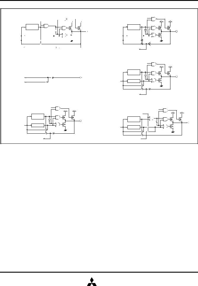
(1) Ports P00/AN0 to P07/AN7 |
|
|
|
|
(4) Port P13/TX0 |
|
||||||
Analog input selection |
Pull-up control bit |
|
|
|
|
|
|
|
|
Pull-up control bit |
|
|
|
||||||||||||
|
|
|
|
|
|
|
|
|
|
|||
|
|
|
|
|
|
|||||||
|
|
|
|
|
|
|
|
|||||
Direction |
direction |
register |
register |
|
|
|
|
|
|
|
|
|
|
|
|
|
|
|
|
|
Data bus |
|
|
Port latch |
|
|
|
|
|
|
|
Data bus |
|
|
Port latch |
|
|
|
|
|
|
|
|
|
|
|
|
|
|
|
|
|
|
|
ADC input |
|
|
|
Timer bi-phase mode input |
|
Analog input selection |
|||||
|
|||||
|
|
||||
|
(5) Ports P14/CNTR0, P15/CNTR1 |
|
|
|
Pull-up control bit |
(2) Port P11/INT0 |
|
Direction |
|
|
register |
Interrupt input |
|
|
Data bus |
Data bus |
Port latch |
|
|
|
(3) Port P12/INT1 |
|
|
Pull-up control bit |
|
Direction |
|
register |
Data bus |
Port latch |
Interrupt input
Timer bi-phase mode input
(6) Port P16/PWM
Pull-up control bit
|
PWM output enable |
|
Direction |
|
register |
Data bus |
Port latch |
PWM output
Fig. 9 Structure of port I/Os (1)
10 |
MITSUBISHI |
|
ELECTRIC |
||
|

MITSUBISHI MICROCOMPUTERS
7630 Group
SINGLE-CHIP 8-BIT CMOS MICROCOMPUTER
(7) Ports P17, P30, P33, P34 |
|
|
Pull-up control bit |
|
Direction |
|
register |
Data bus |
Port latch |
(8) Port P20/SIN |
|
|
Pull-up control bit |
|
SIO Port Select |
|
Direction |
|
register |
Data bus |
Port latch |
SIO1 input |
|
(9) Port P21/SOUT
Pull-up control bit
SIO port selection bit |
|
Transmit complete signal |
|
|
Direction |
|
register |
Data bus |
Port latch |
SIO output
(10) Port P22/SCLK
Pull-up control bit
Clock selection bit |
|
|
Port selection bit |
|
|
|
direction |
|
|
register |
|
Data bus |
Port latch |
|
|
SIO clock output |
External clock input |
(11) Port P23/SRDY
Pull-up control bit
SRDY output selection bit |
|
|
Direction |
|
register |
Data bus |
Port latch |
SRDY output
(12) Ports P24/URXD, P27/UCTS |
||
Transmission or reception* in |
Pull-up control bit |
|
|
progress |
|
|
|
|
Transmit or receive* enable bit |
|
|
|
Direction |
|
|
register |
|
Data bus |
Port latch |
|
|
|
URXD or UCTS input |
(13) Ports P25/UTXD, P26/URTS
Transmission or reception** in |
|
|
Pull-up control bit |
|
|
progress |
|
|
|
|
|
Transmit or receive** enable bit |
|
|
Direction |
|
register |
Data bus |
Port latch |
UTXD or URTS output |
|
(*) for UCTS
(**)for URTS
(14)Port P31/CTX
Pull-up control bit
CAN port selection bit |
|
|
Direction |
|
register |
Data bus |
Port latch |
CTX output
(15) Port P32/CRX |
|
CAN dominant level control bit |
|
Pull-up/down control bit |
|
|
Direction |
|
register |
Data bus |
Port latch |
CAN interrupt |
|
|
CRX input |
(16) Ports P40/KW0 to P47/KW7 |
|
Key-on wake-up control bit |
|
Pull-up/down control bit |
|
|
Direction |
|
register |
Data bus |
Port latch |
Key-on wake-up interrupt |
|
Fig. 10 Structure of port I/Os (2)
MITSUBISHI |
|
ELECTRIC |
11 |

MITSUBISHI MICROCOMPUTERS
7630 Group
SINGLE-CHIP 8-BIT CMOS MICROCOMPUTER
Port Pull-up/pull-down Function
Each pin of ports P0 to P4 except P11 is equipped with a programmable pull-up transistor. P32/CRX and P40/KW0 to P47/KW7 are equipped with programmable pull-down transistors as well. The pull-up function of P0 to P3 can be controlled by the corresponding
port pull-up control registers (see Structure of port pull-up/down control registers). The pull-up/down function of ports P32 and P4 can be controlled by the corresponding port pull-up/pull-down registers together with the polarity control register (see Structure of polarity control register).
7 |
0 |
|
Port Pi pull-up control register (address 002816 + i) (i = 0, 2) |
||||||||||||||||
|
|
|
|
|
|
|
|
|
|
|
|
|
|
|
|
|
|
||
|
|
|
|
|
|
|
|
|
|
|
|
|
|
|
|
|
|
PUP0, PUP2 |
|
|
|
|
|
|
|
|
|
|
|
|
|
|
|
|
|
|
|
||
|
|
|
|
|
|
|
|
|
|
|
|
|
|
|
|
|
|
Pij pull-up transistor control bit (j = 0 to 7) |
|
|
|
|
|
|
|
|
|
|
|
|
|
|
|
|
|
|
|
||
|
|
|
|
|
|
|
|
|
|
|
|
|
|
|
|
|
|
0 : Pull-up transistor disabled |
|
|
|
|
|
|
|
|
|
|
|
|
|
|
|
|
|
|
|
1 : Pull-up transistor enabled |
|
7 |
0 |
|
Port P1 pull-up control register (address 002916) |
||||||||||||||||
|
|
|
|
|
|
|
|
|
|
|
|
|
|
|
|
|
|
||
|
|
|
|
|
|
|
|
|
|
|
|
|
|
|
|
|
|
PUP1 |
|
|
|
|
|
|
|
|
|
|
|
|
|
|
|
|
|
|
|
|
|
|
|
|
|
|
|
|
|
|
|
|
|
|
|
|
|
|
|
Not used (“0” when read, do not write “1”) |
|
|
|
|
|
|
|
|
|
|
|
|
|
|
|
|
|
|
|
||
|
|
|
|
|
|
|
|
|
|
|
|
|
|
|
|
|
|
P1j pull-up transistor control bit (j = 2 to 7) |
|
7 |
0 |
|
|||||||||||||||||
|
Port P3 pull-up control register (address 002B16) |
||||||||||||||||||
|
|
|
|
|
|
|
|
|
|
|
|
|
|
|
|
|
|
||
|
|
|
|
|
|
|
|
|
|
|
|
|
|
|
|
|
|
PUP3 |
|
|
|
|
|
|
|
|
|
|
|
|
|
|
|
|
|
|
|
|
|
|
|
|
|
|
|
|
|
|
|
|
|
|
|
|
|
|
|
P3j pull-up transistor control bit (j = 0, 1) |
|
|
|
|
|
|
|
|
|
|
|
|
|
|
|
|
|
|
|
||
|
|
|
|
|
|
|
|
|
|
|
|
|
|
|
|
|
|
P32 pull-up/down transistor control bit |
|
|
|
|
|
|
|
|
|
|
|
|
|
|
|
|
|
|
|
||
|
|
|
|
|
|
|
|
|
|
|
|
|
|
|
|
|
|
P3j pull-up transistor control bit (j = 3, 4) |
|
|
|
|
|
|
|
|
|
|
|
|
|
|
|
|
|
|
|
||
|
|
|
|
|
|
|
|
|
|
|
|
|
|
|
|
|
|
Not used (“0” when read, do not write “1”) |
|
7 |
0 |
|
|||||||||||||||||
|
Port P4 pull-up/down control register (address 002C16) |
||||||||||||||||||
|
|
|
|
|
|
|
|
|
|
|
|
|
|
|
|
|
|
||
|
|
|
|
|
|
|
|
|
|
|
|
|
|
|
|
|
|
PUP4 |
|
|
|
|
|
|
|
|
|
|
|
|
|
|
|
|
|
|
|
|
|
|
|
|
|
|
|
|
|
|
|
|
|
|
|
|
|
|
|
P4j pull-up/down transistor control bit (j = 0 to 7) |
|
|
|
|
|
|
|
|
|
|
|
|
|
|
|
|
|
|
|
||
|
|
|
0 : |
Pull-up/down transistor disabled |
|||||||||||||||
|
|
|
1 : |
Pull-up/down transistor enabled |
|||||||||||||||
|
|
||||||||||||||||||
Fig. 11 Structure of port pull-up/down control registers |
|
||||||||||||||||||
|
|
|
|
|
|||||||||||||||
7 |
0 |
|
|
|
|||||||||||||||
Polarity control register (address 002F16)
PCON
Key-on wake-up polarity control bit 0 : Low level active
1 : High level active
CAN module dominant level control bit 0 : Low level dominant
1 : High level dominant
Not used (undefined when read)
Fig. 12 Structure of polarity control register
12 |
MITSUBISHI |
|
ELECTRIC |
||
|

MITSUBISHI MICROCOMPUTERS
7630 Group
SINGLE-CHIP 8-BIT CMOS MICROCOMPUTER
Port Overvoltage Application
When configured as input ports, P1 to P4 may be subjected to overvoltage (VI > VCC) if the input current to the applicable port is limited to the specified values (see “Table 8:”). Use a serial resistor of appropriate size to limit the input current. To estimate the resistor value, assume the port voltage to be VCC at overvoltage condition.
Notes:
•Subjecting ports to overvoltage may effect the supply voltage. Assure to keep VCC and VSS within the target limits.
•Avoid to subject ports to overvoltage causing VCC to rise above
5.5V.
•The overvoltage condition causing input current flowing through the internal port protection circuits has a negative effect on the ports noise immunity. Therefore, careful and intense testing of the target system’s noise immunity is required. Refer to the “countermeasures against noise” of the corresponding users manual.
•Port P0 must not be subjected to overvoltage conditions.
MITSUBISHI |
|
ELECTRIC |
13 |

MITSUBISHI MICROCOMPUTERS
7630 Group
SINGLE-CHIP 8-BIT CMOS MICROCOMPUTER
INTERRUPTS
There are 24 interrupts: 6 external, 17 internal, and 1 software.
Interrupt Control
Each interrupt except the BRK instruction interrupt has both an interrupt request bit and an interrupt enable bit, and is controlled by the interrupt disable flag. An interrupt occurs when the corresponding interrupt request and enable bits are “1” and the interrupt disable flag is “0”. Interrupt enable bits can be cleared or set by software. Interrupt request bits can be cleared by software but cannot be set by software. The BRK instruction interrupt and reset cannot be disabled with any flag or bit. The I flag disables all interrupts except the BRK instruction interrupt and reset. If several interrupt requests occur at the same time, the interrupt with the highest priority is accepted first.
Interrupt Operation
Upon acceptance of an interrupt, the following operations are automatically performed.
1.The processing being executed is stopped.
2.The contents of the program counter and processor status register are automatically pushed onto the stack.
3.Concurrently with the push operation, the interrupt jump destination address is read from the vector table into the program counter.
4.The interrupt disable flag is set and the corresponding interrupt request bit is cleared.
Notes on use
When the active edge of an external interrupt (INT0, INT1, CNTR0, CNTR1, CWKU or KOI) is changed, the corresponding interrupt request bit may also be set. Therefore, take the following sequence.
(1)Disable the external interrupt which is selected.
(2)Change the active edge in interrupt edge selection register.
(in the case of CNTR0: Timer X mode register; in the case of CNTR1: Timer Y mode register)
(3)Clear the interrupt request bit to “0”.
(4)Enable the external interrupt which is selected.
14 |
MITSUBISHI |
|
ELECTRIC |
||
|

|
|
|
|
MITSUBISHI MICROCOMPUTERS |
||
|
|
|
|
|
7630 Group |
|
|
|
|
|
SINGLE-CHIP 8-BIT CMOS MICROCOMPUTER |
||
|
|
|
|
|
|
|
. |
|
|
|
|
|
|
Table 3: Interrupt vector addresses and priority |
|
|
|
|||
|
|
|
|
|
|
|
|
|
Vector Address (Note 1) |
Interrupt Request Generating |
|
||
Interrupt source |
Priority |
|
|
Remarks |
||
High |
Low |
Conditions |
||||
|
|
|
||||
|
|
|
|
|||
|
|
|
|
|
|
|
Reset (Note 2) |
1 |
FFFB16 |
FFFA16 |
At Reset |
Non-maskable |
|
|
|
|
|
|
|
|
Watchdog timer |
2 |
FFF916 |
FFF816 |
At Watchdog timer underflow |
Non-maskable |
|
|
|
|
|
|
|
|
INT0 |
3 |
FFF716 |
FFF616 |
At detection of either rising or falling |
External Interrupt |
|
edge of INT0 interrupt |
(active edge selectable) |
|||||
|
|
|
|
|||
INT1 |
4 |
FFF516 |
FFF416 |
At detection of either rising or falling |
External Interrupt |
|
edge of INT1 interrupt |
(active edge selectable) |
|||||
|
|
|
|
|||
CAN successful |
5 |
FFF316 |
FFF216 |
At CAN module successful |
Valid when CAN module is |
|
transmit |
transmission of message |
activated and request transmit |
||||
|
|
|
||||
|
|
|
|
|
|
|
CAN successful |
6 |
FFF116 |
FFF016 |
At CAN module successful reception |
Valid when CAN module is |
|
receive |
of message |
activated |
||||
|
|
|
||||
|
|
|
|
|
|
|
CAN overrun |
7 |
FFEF16 |
FFEE16 |
If CAN module receives message |
Valid when CAN module is |
|
when receive buffers are full. |
activated |
|||||
|
|
|
|
|||
|
|
|
|
|
|
|
CAN error |
8 |
FFED16 |
FFEC16 |
When CAN module enters into error |
Valid when CAN module is |
|
passive |
passive state |
active |
||||
|
|
|
||||
|
|
|
|
|
|
|
CAN error bus off |
9 |
FFEB16 |
FFEA16 |
When CAN module enters into bus |
Valid when CAN module is |
|
off state |
active |
|||||
|
|
|
|
|||
|
|
|
|
|
|
|
CAN wake up |
10 |
FFE916 |
FFE816 |
When CAN module wakes up via |
|
|
CAN bus |
|
|||||
|
|
|
|
|
||
|
|
|
|
|
|
|
Timer X |
11 |
FFE716 |
FFE616 |
At Timer X underflow or overflow |
|
|
|
|
|
|
|
|
|
Timer Y |
12 |
FFE516 |
FFE416 |
At Timer Y underflow |
|
|
|
|
|
|
|
|
|
Timer 1 |
13 |
FFE316 |
FFE216 |
At Timer 1 underflow |
|
|
|
|
|
|
|
|
|
Timer 2 |
14 |
FFE116 |
FFE016 |
At Timer 2 underflow |
|
|
|
|
|
|
|
|
|
Timer 3 |
15 |
FFDF16 |
FFDE16 |
At Timer 3 underflow |
|
|
|
|
|
|
|
|
|
CNTR0 |
16 |
FFDD16 |
FFDC16 |
At detection of either rising or falling |
External Interrupt |
|
edge in CNTR0 input |
(active edge selectable) |
|||||
|
|
|
|
|||
CNTR1 |
17 |
FFDB16 |
FFDA16 |
At detection of either rising or falling |
External Interrupt |
|
edge in CNTR1 input |
(active edge selectable) |
|||||
|
|
|
|
|||
UART receive |
18 |
FFD916 |
FFD816 |
At completion of UART receive |
Valid when UART is selected |
|
|
|
|
|
|
|
|
UART transmit |
19 |
FFD716 |
FFD616 |
At completion of UART transmit |
Valid when UART is selected |
|
|
|
|
|
|
|
|
UART transmit |
20 |
FFD516 |
FFD416 |
At UART transmit buffer empty |
Valid when UART is selected |
|
buffer empty |
||||||
|
|
|
|
|
||
|
|
|
|
|
|
|
UART receive |
21 |
FFD316 |
FFD216 |
When UART reception error occurs. |
Valid when UART is selected |
|
error |
||||||
|
|
|
|
|
||
|
|
|
|
|
|
|
Serial I/O |
22 |
FFD116 |
FFD016 |
At completion of serial I/O data |
Valid when serial I/O is |
|
transmit and receive |
selected |
|||||
|
|
|
|
|||
|
|
|
|
|
|
|
A-D conversion |
23 |
FFCF16 |
FFCE16 |
At completion of A-D conversion |
|
|
|
|
|
|
|
|
|
Key-on wake-up |
24 |
FFCD16 |
FFCC16 |
At detection of either rising or falling |
External Interrupt |
|
edge of P4 input |
(active edge selectable) |
|||||
|
|
|
|
|||
|
|
|
|
|
|
|
BRK instruction |
25 |
FFCB16 |
FFCA16 |
At BRK instruction execution |
Non-maskable |
|
|
|
|
|
|
|
|
Notes 1: Vector addresses contain interrupt jump destination address |
|
|||||
2: Reset function in the same way as an interrupt with the highest priority |
|
|||||
MITSUBISHI |
|
ELECTRIC |
15 |
 Loading...