


®
867B,863
Graphical Multimeters
Service Manual
PN 689312
December 1997
© 1997 Fluke Corporation, All rights reserved. Printed in U.S.A. All product names are trademarks of their respective companies.
Table of Contents
Chapter |
|
Title |
Page |
1 |
Introduction and Specifications .......................................................................................... |
1-1 |
|
|
1-1.. |
Introduction ............................................................................................................. |
1-3 |
|
1-2. |
Description .............................................................................................................. |
1-3 |
|
1-3. |
Power Requirements ............................................................................................... |
1-3 |
|
1-4. |
Options, Accessories and Related Equipment ....................................................... |
1-4 |
|
1-5. |
Operating Instructions ............................................................................................ |
1-4 |
|
1-6. |
Obtaining Service ................................................................................................... |
1-4 |
|
1-7. |
Conventions Used in This Manual ......................................................................... |
1-5 |
|
1-8. |
Chapter Contents .................................................................................................... |
1-5 |
|
1-9. |
Specifications .......................................................................................................... |
1-6 |
2 |
Theory of Operation............................................................................................................. |
2-1 |
|
|
2-1. |
Introduction ............................................................................................................. |
2-3 |
|
2-2. |
Start-Up Sequence .................................................................................................. |
2-3 |
|
2-3. |
Function Selection .................................................................................................. |
2-3 |
|
2-4. |
Power Supply .......................................................................................................... |
2-4 |
|
2-5. |
Power Supply Input Voltages ................................................................................. |
2-4 |
|
2-6. |
Power Supply Output Voltages and Currents ........................................................ |
2-6 |
|
2-7. |
Power Supply Signals ............................................................................................ |
2-7 |
|
2-8. |
Power ON/OFF Requirements ............................................................................... |
2-8 |
|
2-9. |
NiCd Charging Requirements ................................................................................ |
2-8 |
|
2-10. |
Battery and Line Level Detection .......................................................................... |
2-8 |
|
2-11. |
Power Supply Functional Blocks ........................................................................... |
2-9 |
|
2-12. |
Input Power Selector (A) ........................................................................................ |
2-9 |
|
2-13. |
Boost Preregulator (B) ............................................................................................ |
2-10 |
|
2-14. |
Battery Charger (C) ................................................................................................ |
2-10 |
|
2-15. |
DC-DC Converter (D) ............................................................................................ |
2-12 |
|
2-16. |
Backlight Current Sink (E) ..................................................................................... |
2-12 |
|
2-17. |
Power Switch Circuitry (F) .................................................................................... |
2-12 |
|
2-18. |
LCD Contrast Control (G) ...................................................................................... |
2-12 |
|
2-19. |
Power-On Reset Circuit (H) ................................................................................... |
2-12 |
|
2-20. |
Linear Post Regulators (I) ....................................................................................... |
2-13 |
|
2-21. |
Input Overload Protection ...................................................................................... |
2-13 |
i
|
|
|
Contents (continued) |
|
2-22. |
Volt/Ohms Input Protection ................................................................................... |
2-13 |
|
2-23. |
External Trigger and Logic Activity Input Protection ........................................... |
2-14 |
|
2-24. |
Amps / mA / µA Input Protection .......................................................................... |
2-14 |
|
2-25. |
Input Signal Conditioning ...................................................................................... |
2-14 |
|
2-26. |
AC Volts ................................................................................................................. |
2-14 |
|
2-27. |
DC Volts ................................................................................................................. |
2-16 |
|
2-28. |
mV DC .................................................................................................................... |
2-16 |
|
2-29. |
Ohms ....................................................................................................................... |
2-17 |
|
2-30. |
Diode Test ............................................................................................................... |
2-17 |
|
2-31. |
Capacitance ............................................................................................................. |
2-17 |
|
2-32. |
mA/µA .................................................................................................................... |
2-18 |
|
2-33. |
Amps ....................................................................................................................... |
2-18 |
|
2-34. |
Waveform Processing ............................................................................................. |
2-19 |
|
2-35. |
Overview ................................................................................................................. |
2-19 |
|
2-36. |
Detailed Description ............................................................................................... |
2-19 |
|
2-37. |
Waveform Triggering ............................................................................................. |
2-20 |
|
2-38. |
Overview ................................................................................................................. |
2-20 |
|
2-39. |
Dual Trigger ............................................................................................................ |
2-20 |
|
2-40. |
Single Trigger ......................................................................................................... |
2-21 |
|
2-41. |
External Trigger ...................................................................................................... |
2-21 |
|
2-42. |
Glitch Capture ......................................................................................................... |
2-22 |
|
2-43. |
Single Shot .............................................................................................................. |
2-22 |
|
2-44. |
Frequency Trigger .................................................................................................. |
2-22 |
|
2-45. |
Logic Activity Trigger ............................................................................................ |
2-22 |
|
2-46. |
Peak Hold ................................................................................................................ |
2-22 |
|
2-47. |
Auto Diode .............................................................................................................. |
2-22 |
|
2-48. |
Component Test ...................................................................................................... |
2-23 |
|
2-49. |
Digital Circuitry ...................................................................................................... |
2-24 |
|
2-50. |
RS-232 Serial Port .................................................................................................. |
2-24 |
3 |
Maintenance .......................................................................................................................... |
3-1 |
|
|
3-1. |
Introduction ............................................................................................................. |
3-3 |
|
3-2. |
Warranty Repairs and Shipping Information ......................................................... |
3-3 |
|
3-3. |
Static-Safe Handling ............................................................................................... |
3-3 |
|
3-4. |
Cleaning .................................................................................................................. |
3-4 |
|
3-5. |
Disassembly ............................................................................................................ |
3-4 |
|
3-6. |
Reasssembly ............................................................................................................ |
3-7 |
|
3-7. |
Replacing the 440 mA Fuse ................................................................................... |
3-9 |
|
3-8. |
Replacing the 11A (High Energy) Fuse ................................................................. |
3-9 |
4 |
Perfomance Testing and Calibration ................................................................................. |
4-1 |
|
|
4-1. |
Introduction ............................................................................................................. |
4-3 |
|
4-2. |
Required Test Equipment ....................................................................................... |
4-3 |
|
4-3. |
Alternative Test Equipment (Fluke 5500A) ........................................................... |
4-3 |
|
4-4. |
Performance Tests .................................................................................................. |
4-4 |
|
4-5. |
mV DC Test ............................................................................................................ |
4-4 |
|
4-6. |
DC Volts Test ......................................................................................................... |
4-6 |
|
4-7. |
Diode Test ............................................................................................................... |
4-7 |
|
4-8. |
AC Volts Test ......................................................................................................... |
4-8 |
|
4-9. |
Ohms and Conductance Tests ................................................................................ |
4-10 |
|
4-10. |
Capacitance Test ..................................................................................................... |
4-11 |
|
4-11. |
Frequency Test ........................................................................................................ |
4-12 |
|
4-12. |
Duty Cycle Test ...................................................................................................... |
4-14 |
|
4-13. |
Logic Test (867B Only) .......................................................................................... |
4-15 |
ii
|
|
|
Contents (continued) |
|
4-14. |
Amps Tests ............................................................................................................. |
4-16 |
|
4-15. |
Peak Hold Test ........................................................................................................ |
4-19 |
|
4-16. |
Component Test (867B Only) ................................................................................ |
4-19 |
|
4-17. |
Rel Test/Touch Hold Test ...................................................................................... |
4-20 |
|
4-18. |
Glitch Capture Test ................................................................................................. |
4-21 |
|
4-19. |
External Trigger Test .............................................................................................. |
4-21 |
|
4-20. |
Calibration ............................................................................................................... |
4-22 |
|
4-21. |
Measuring the System Resistance .......................................................................... |
4-22 |
|
4-22. |
Starting Calibration Mode on the GMM ................................................................ |
4-22 |
|
4-23. |
mV DC Calibration ................................................................................................. |
4-23 |
|
4-24. |
DC Volts Calibration .............................................................................................. |
4-24 |
|
4-25. |
DC mAuA Calibration ............................................................................................ |
4-24 |
|
4-26. |
DC Amps Calibration ............................................................................................. |
4-24 |
|
4-27. |
Ohms/nS Calibration .............................................................................................. |
4-25 |
|
4-28. |
Modifying the Displayed Value ............................................................................. |
4-25 |
|
4-29. |
Ohms Calibration .................................................................................................... |
4-26 |
|
4-30. |
AC Volts Calibration .............................................................................................. |
4-27 |
|
4-31. |
AC mA(A Calibration ............................................................................................ |
4-27 |
|
4-32. |
AC Amps Calibration ............................................................................................. |
4-27 |
|
4-33. |
Internal Constants Calibration ................................................................................ |
4-28 |
|
4-34. |
Setting LCD Voltage .............................................................................................. |
4-28 |
5 |
List of Replaceable Parts ..................................................................................................... |
5-1 |
|
|
5-1. |
Introduction ............................................................................................................. |
5-3 |
|
5-2. |
How To Obtain Parts .............................................................................................. |
5-3 |
|
5-3. |
Manual Status Information ..................................................................................... |
5-3 |
|
5-4. |
Newer Instruments .................................................................................................. |
5-3 |
|
5-5. |
Service Centers ....................................................................................................... |
5-4 |
|
5-6. |
Parts ......................................................................................................................... |
5-4 |
6 |
Schematic Diagrams............................................................................................................. |
6-1 |
|
iii
List of Tables
Table |
Title |
Page |
1-1. |
Power Sources ......................................................................................................... |
1-4 |
1-2. |
Accessories Included with Each GMM ................................................................... |
1-4 |
2-1. |
Power Supply Inputs................................................................................................ |
2-4 |
2-3. |
Power Supply Signals.............................................................................................. |
2-7 |
2-4. |
Power Source Detection .......................................................................................... |
2-9 |
2-5. |
Average Converter................................................................................................... |
2-15 |
2-6. |
RMS Converter (U3) ............................................................................................... |
2-16 |
2-7. |
Test Point Voltages.................................................................................................. |
2-16 |
2-8. |
Ohms Ratiometric Measurements ........................................................................... |
2-17 |
2-9. |
Amps Measurement Paths ....................................................................................... |
2-18 |
4-1. |
Recommended Test Equipment............................................................................... |
4-4 |
4-2. |
mV DC Performance Test ....................................................................................... |
4-4 |
4-3. |
DC Volts Performance Test..................................................................................... |
4-6 |
4-4. |
Diode Test Performance Test .................................................................................. |
4-7 |
4-5. |
AC Volts RMS Performance Test ........................................................................... |
4-8 |
4-6. |
AC Volts Average Performance Test ...................................................................... |
4-8 |
4-7. |
Ohms Performance Test .......................................................................................... |
4-10 |
4-8. |
Conductance Performance Test............................................................................... |
4-10 |
4-9. |
Capacitance Performance Test ................................................................................ |
4-11 |
4-10. |
Frequency (AC Volts) Performance Test ................................................................ |
4-12 |
4-11. |
Frequency (mAuA) Performance Test .................................................................... |
4-12 |
4-12. |
Duty Cycle Performance Test.................................................................................. |
4-14 |
4-13. |
Logic Performance Test .......................................................................................... |
4-15 |
4-14. |
DC Amps Performance Test.................................................................................... |
4-16 |
4-15. |
AC Amps RMS Performance Test .......................................................................... |
4-16 |
4-16. |
AC Amps Average Performance Test ..................................................................... |
4-17 |
4-17. |
Peak Hold Performance Test ................................................................................... |
4-19 |
4-18. |
Component Test Performance Test ......................................................................... |
4-19 |
4-19. |
Rel Performance Test .............................................................................................. |
4-20 |
4-20. |
Touch Hold Performance Test................................................................................. |
4-20 |
4-21. |
Glitch Capture Performance Test ............................................................................ |
4-21 |
4-22. |
External Trigger Performance Test ......................................................................... |
4-21 |
5-1. |
860 Series Final Assembly ...................................................................................... |
5-5 |
5-2. |
A1 Main PCA.......................................................................................................... |
5-8 |
iv
List of Figures
Figure |
Title |
Page |
1-1. |
Temperature and Humidity...................................................................................... |
1-7 |
2-1. |
Block Diagram......................................................................................................... |
2-5 |
2-2. |
Power Supply Blocks .............................................................................................. |
2-11 |
2-3. |
Keypad Connections................................................................................................ |
2-25 |
3-1. |
Disassembly............................................................................................................. |
3-5 |
3-2. |
Reassembly.............................................................................................................. |
3-8 |
3-3. |
Replacing the 400 mA Fuse..................................................................................... |
3-9 |
4-1. |
Configuration 1 (mV DC) ....................................................................................... |
4-5 |
4-2. |
Configuration 2 (DC Volts)..................................................................................... |
4-6 |
4-3. |
Configuration 6 (AC Volts)..................................................................................... |
4-9 |
4-4. |
Configuration 5 (Ohms) .......................................................................................... |
4-11 |
4-5. |
Configuration 7 (PM5139) ...................................................................................... |
4-13 |
4-6. |
Configuration 7 (PM5139) ...................................................................................... |
4-14 |
4-7. |
Configuration 9 (PM5139) ...................................................................................... |
4-16 |
4-8. |
Configuration 3 (mAuA, DC and AC) .................................................................... |
4-17 |
4-9. |
Configuration 4 (Amps, DC and AC)...................................................................... |
4-18 |
4-10. |
Configuration 8 (Component Test).......................................................................... |
4-19 |
4-11. |
Initiating Calibration ............................................................................................... |
4-22 |
4-12. |
Entering Calibration Mode ...................................................................................... |
4-23 |
4-13. |
Modifying the Displayed Value .............................................................................. |
4-25 |
4-14. |
Ohms Calibration..................................................................................................... |
4-26 |
5-1. |
860 Series Final Assembly ..................................................................................... |
5-7 |
5-2. |
A1 Main PCA.......................................................................................................... |
5-16 |
v
Chapter 1
Introduction and Specifications
|
Title |
Page |
1-1. |
Introduction............................................................................................. |
1-3 |
1-2. |
Description .............................................................................................. |
1-3 |
1-3. |
Power Requirements ............................................................................... |
1-3 |
1-4. |
Options, Accessories and Related Equipment......................................... |
1-4 |
1-5. |
Operating Instructions............................................................................. |
1-4 |
1-6. |
Obtaining Service.................................................................................... |
1-4 |
1-7. |
Conventions Used in This Manual.......................................................... |
1-5 |
1-8. |
Chapter Contents..................................................................................... |
1-5 |
1-9. |
Specifications .......................................................................................... |
1-6 |
1-1
|
Introduction and Specifications |
1 |
|
Introduction |
|
Introduction |
1-1. |
|
This manual includes the following information:
•Specifications (Chapter 1):
•Theory of Operation (Chapter 2):
•General Maintenance (Chapter 3):
•Performance Testing and Calibration procedures (Chapter 4):
•List of Replaceable Parts (Chapter 5):
•Schematic Diagrams and component locators (Chapter 6):
The information in this manual is applicable to both the 867B and 863 models unless otherwise indicated.
Description |
1-2. |
The Fluke 867B and 863 Graphical Multimeters (GMMs) provide full digital multimeter (DMM) capabilities along with graphical waveform displays and trend plotting. Model 867B also provides component testing and logic activity testing.
Power Requirements |
1-3. |
The GMM can be powered with the Battery Eliminator or with 6 “AA” (ANSI/NEDAL40) alkaline cells. New alkaline batteries provide a minimum of 6 hours of continuous operation. You can also use the NiCd battery pack. Depending on battery condition, a fully charged NiCd battery pack provides 8 hours (typical) or less of continuous operation. Internal charging is available on Model 867B.
1-3

867B,863
Service Manual
Table 1-1. Power Sources
|
|
Model 867B |
Model 863 |
|
|
|
|
|
Battery Eliminator Operation |
• |
• |
|
|
|
|
|
Alkaline Battery Operation (6 AA, |
• |
• |
|
ANSI/NEDA-L40) |
|
|
|
|
|
|
|
NiCd Battery Pack Operation (with |
• |
|
|
internal charging) |
|
|
|
|
|
|
|
NiCd Battery Pack Operation (with |
|
• |
|
external charging) |
|
|
|
|
|
|
Options, Accessories and Related Equipment |
1-4. |
||
Accessories supplied with Fluke 867B and 863 GMMs are listed in Table 1-2.
Table 1-2. Accessories Included with Each GMM
|
|
Model 867B |
Model 863 |
|
|
|
|
|
TL70A Test Leads (2) |
• |
• |
|
|
|
|
|
Battery Eliminator |
• |
|
|
|
|
|
|
NiCd Battery Pack |
• |
|
|
|
|
|
Operating Instructions |
|
1-5. |
|
Operating instructions for the Fluke 867B and 863 Graphical Multimeters can be found in the Users Manual. For ordering information, see “How to Obtain Parts” in Chapter 5.
Obtaining Service |
1-6. |
A GMM under warranty will be promptly repaired or replaced (at Fluke’s option) and returned at no charge. See the registration card for warranty terms. If the warranty has expired, the GMM will be repaired and returned for a fixed fee. Contact the nearest Service Center for information and prices. A list of U.S. and International Service Centers is available on the World Wide Web at www.fluke.com. Refer to Chapter 3 for a list of Fluke telephone numbers.
1-4
|
Introduction and Specifications |
1 |
|
Conventions Used in This Manual |
|
Conventions Used in This Manual |
1-7. |
|
The following conventions are used in this manual:
•“GMM” refers to all Graphical Multimeter models in the 860 Series.
•“863” and “867B” are specifically mentioned where a description does not apply to all models in the 860 Series.
•A “pca” is a printed circuit board and its attached parts.
•A pin or connection on a component is specified by the component reference designator, a dash (-), and a pin number. For example, component U30, pin 92 would be U30-92.
Chapter Contents |
1-8. |
The chapters in this manual document service for the GMM as follows:
•Chapter 1. Introduction and Specifications describes the Service Manual, explains special terminology and conventions, and provides complete GMM specifications.
•Chapter 2. Theory of Operation describes the GMM’s circuitry in terms of functional blocks, with a description of each block’s role in overall operation. A detailed circuit description is then given for each block.
•Chapter 3. General Maintenance provides information on general maintenance, handling precautions and disassembly instructions. Instructions covering warranty repairs and shipping the instrument to a service center are also contained in this chapter.
•Chapter 4. Performance Testing and Calibration contains information on required test equipment, performance test procedures and calibration of the GMM.
•Chapter 5. List of Replaceable Parts describes parts used in the GMM along with ordering information.
•Chapter 6. Schematic Diagrams contains a full set of schematic diagrams and component locators.
1-5
867B,863
Service Manual
Specifications |
1-9. |
General
Display: LCD - Dot Matrix, 240 X 200 pixels
Fluke 867B: Transmissive, Backlit
Fluke 863: Reflective
Temperature Operating: 0°C to 50°C (See Figure 1-1.)
Storage: -20°C to 60°C (Batteries Removed)
Charging: 0 to 45°C
Temperature Coefficient: (0.1 X % Accuracy) per °C (0°C to 18°C and 28°C to 59°C)
Relative Humidity: 0% to 90% non-condensing
Altitude Operating/Non-operating: 6,562 ft. (2,000 meters)/ 40,000 ft. (12,200 meters)
Input Impedance: 10 MΩ
Shock and Vibration: per MIL-T-28800, class 3, sinusoidal, non-operating
Dimensions: 5.4 x 9.7 x 2.7 in. (137 x 246 x 68 mm)
Weight: 3 lbs (1.35 kg)
Battery Operating Time (backlight off or low)
Alkaline: 8 hours typical
NiCd:
863: |
10 hours typical |
867B: |
8 hours typical |
Battery Recharge Time: 16 hours minimum from full discharge
Drip Proof Case: per IEC 529; IP 52, Drip Proof
Safety: Designed to meet IEC 1010-1 Category III, UL3111, CSA-C22.2. 1010-1-92, CE and TUV requirements
Certification:
Electromagnetic Interference
RF Emissions EN-50081-1 Commercial Limits
VFG 243-1991
FCC Part 15 Class B,
RF Susceptibility: EN 50082-1 Industrial Limits
1-6
Introduction and Specifications |
1 |
Specifications |
|
100 |
|
|
|
|
|
|
|
|
|
90 |
|
|
|
|
|
|
|
|
|
80 |
|
|
|
|
|
|
|
|
|
70 |
|
|
|
|
|
|
|
|
|
60 |
|
|
|
|
|
|
|
|
%RH |
50 |
|
|
|
|
|
|
|
|
|
|
|
|
|
|
|
|
|
|
|
40 |
|
|
|
|
|
|
|
|
|
30 |
|
|
|
|
|
|
|
|
|
20 |
|
|
|
|
|
|
|
|
|
10 |
|
|
|
|
|
|
|
|
|
0 |
|
|
|
|
|
|
|
|
|
-20 |
0 |
20 |
40 |
60 |
80 |
100 |
120 |
140 |
|
|
-4 |
|
32 |
|
|
|
|
|
|
|
|
|
Temperature (°F) |
|
|
|
||
|
|
-20 |
|
0 |
|
30 |
40 |
50 |
60 |
|
|
|
|
Temperature (°C) |
|
|
|
||
|
|
|
|
= Storage (-20°C — 60°C) |
|
|
|||

 = Normal Operation (0°C — 50°C)
os1f.eps
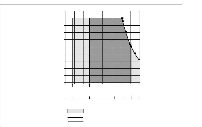
Figure 1-1. Temperature and Humidity
Power
|
Fluke 867B |
Fluke 863 |
|
|
|
|
|
Battery Eliminator/Charger |
Yes |
Optional Eliminator only |
|
|
|
|
|
NiCd Battery Pack |
Yes |
Optional BP7217 Battery |
|
Pack |
|||
|
|
||
|
|
Optional BC7210 Ext. |
|
|
|
Charger |
|
|
|
|
|
Alkaline Batteries 6 AA Cells |
Optional Customer Supplied |
Yes |
|
|
|
|
|
Battery Life: NiCad |
≥8 hrs (supplied) |
≥10 hrs (optional) |
|
Alkaline |
≥8 hrs (optional) |
≥8 hrs (supplied) |
|
|
|
|
1-7

867B,863
Service Manual
Resolution and Accuracy
The following specifications apply within 1 year of calibration when operating in a temperature range of 18°C (64°F) to 28°C (82°F).
AC Volts (True RMS, AC-Coupled) [±(percent of reading + counts)]
|
|
|
|
Frequency |
|
|
|
Range |
Res. |
|
|
|
|
|
|
20 - |
50 - |
1 kHz - |
30 kHz- |
100kHz- |
200 kHz- |
||
|
|
50 Hz |
1 kHz |
30 kHz |
100 kHz |
200kHz |
300 kHz |
|
|
|
|
|
|
|
|
300.00 mV |
0.01 mV |
1.5% + 10 |
0.5% + 10 |
0.5% + 10 |
4% + 200 |
8% + 200 |
10%+ 200 |
|
|
0.19 dB |
0.10 dB |
0.10 dB |
1.39 dB |
1.68 dB |
1.82 dB |
3.0000V |
0.1 mV |
1.5% + 10 |
0.5% + 10 |
0.5% + 10 |
4% + 200 |
8% + 200 |
10%+ 200 |
|
|
0.19 dB |
0.10 dB |
0.10 dB |
1.39 dB |
1.68 dB |
1.82 dB |
30.000V |
1 mV |
1.5% + 10 |
0.5% + 10 |
0.5% + 10 |
4% + 200 |
8% + 200 |
10%+ 200 |
|
|
0.19 dB |
0.10 dB |
0.10 dB |
1.39 dB |
1.68 dB |
1.82 dB |
300.00V |
10 mV |
1.5% + 10 |
0.5% + 10 |
0.5% + 10 |
4% + 200 |
8% + 200 |
10%+ 200 |
|
|
0.19 dB |
0.10 dB |
0.10 dB |
1.39 dB |
1.68 dB |
1.82 dB |
1000.0V |
100 mV |
1.5% + 10 |
1.5% + 10 |
NA |
NA |
NA |
NA |
|
|
0.19 dB |
0.19 dB |
||||
|
|
|
|
|
|
||
300 mV - 300V ranges ≥3:1, 1000V range ≥3:1 decreasing to ≥1.41:1 as input voltage increases to 1000V (peak voltage not to exceed 1414V).
Measurement Range: 300 mV range from 10% to 100% of range. 3V - 1000V ranges from 5% to 100% of range.
For frequencies > 100 kHz 30% to 100% of range (all ranges).
1-8

|
|
|
|
|
Introduction and Specifications |
1 |
||
|
|
|
|
|
|
Specifications |
||
|
AC Volts - Average Responding AC Coupled [±(percent of reading + counts)] |
|
||||||
|
|
|
|
|
|
|
|
|
|
|
|
|
Frequency |
|
|
|
|
|
Range |
Res. |
|
|
|
|
|
|
|
20 - 50 Hz |
50 - 1 kHz |
1 kHz - 30 kHz |
30 kH - 50 kHz |
|
|
||
|
|
|
|
|
|
|
|
|
|
300.0 mV |
0.1 mV |
1.5% + 4 |
0.5% + 4 |
0.5% + 4 |
2% + 4 |
|
|
|
|
|
0.25 dB |
0.16 dB |
0.16 dB |
0.25 dB |
|
|
|
|
|
|
|
|
|
|
|
|
3.000V |
1 mV |
1.5% + 4 |
0.5% + 4 |
0.5% + 4 |
2% + 4 |
|
|
|
|
|
0.25 dB |
0.16 dB |
0.16 dB |
0.25 dB |
|
|
|
|
|
|
|
|
|
|
|
|
30.00V |
10 mV |
1.5% + 4 |
0.5% + 4 |
0.5% + 4 |
2% + 4 |
|
|
|
|
|
0.25 dB |
0.16 dB |
0.16 dB |
0.25 dB |
|
|
|
|
|
|
|
|
|
|
|
|
300.0V |
100 mV |
1.5% + 4 |
0.5% + 4 |
0.5% + 4 |
2% + 4 |
|
|
|
|
|
0.25 dB |
0.16 dB |
0.16 dB |
0.25 dB |
|
|
|
|
|
|
|
|
|
|
|
|
1000V |
1 V |
1.5% + 4 |
1.5% + 4 |
NA |
NA |
|
|
|
|
|
0.25 dB |
0.25 dB |
|
|
|
|
Input Impedance: 1.11 MΩ ±1% in series with 0.1 µF
Volts-Hertz Product: 2 x 10⁷
Common Mode Rejection: >60 dB at 50 Hz and 60 Hz (1 kΩ unbalance)
Common Mode Volts-Hertz Product: 1 x 10⁷
dBm Reference: 2, 4, 8, 16, 50, 75, 93, 110, 125, 135, 150, 300, 600, 900, 1000, and 1200Ω
Overload Protection: 1000V rms
DC Volts [±(percent of reading + counts)]
Function |
Range |
Res. |
Fluke 867B |
Fluke 863 |
|
|
|
|
|
mV DC |
300.00 mV |
0.01 mV |
0.025% + 2 |
0.04% + 2 |
|
3000.0 mV |
0.1 mV |
0.025% + 2 |
0.04% + 2 |
|
30.000V |
0.001 V |
0.025% + 2 |
0.04% + 2 |
V DC |
300.00V |
0.01 V |
0.025% + 2 |
0.04% + 2 |
|
1000.0V |
0.1 V |
0.025% + 2 |
0.04% + 2 |
Input Impedance: V DC-10 MΩ, mV DC-10 MΩ, mV DC Hi-Z ->1000 MΩ
Normal Mode Rejection: >60 dB at 50 Hz or 60 Hz
Common Mode Rejection: >120 dB a dc, >90 dB at 50 Hz and 60 Hz (1 kΩ unbalance)
Overload Protection: 1000 V rms
Maximum Allowable Peak AC + DC Voltage (without causing a reading error) 300 mV, 3000 mV ranges: 15V
30V range: 1000V; 300V, 1000V ranges: 1414V
1-9

867B,863
Service Manual
Diode Test (Manual)
Range: 3V
Resolution: 0.0001V
Accuracy: ±0.05% of reading + 2 digits
Open Circuit Voltage: 3.1V
Diode Test (Auto)
Accuracy: 20%
Current Ranges
Ranges for True |
True RMS |
|
Ranges for Average |
|
|
Measurement Range |
|
Maximum |
|
||
RMS AC Current |
|
Responding AC |
Fuse |
||
(% Range to % Full |
|
Burden |
|||
and DC Current |
|
Current |
Protection |
||
Scale) |
|
Voltage |
|||
|
|
|
|
||
300.00 A1 |
5% - 100% |
|
300.0 A |
0.03V |
440 mA @ |
|
|
|
|
|
1000V |
3000.0 A1 |
5% - 100% |
|
3000 A |
0.3V |
440 mA @ |
|
|
|
|
|
1000V |
30.000 mA |
5% - 100% |
|
30.00 mA |
0.03V |
440 mA @ |
|
|
|
|
|
1000V |
300.00 mA |
5% - 100% |
|
300.0 mA |
0.3V |
440 mA @ |
|
|
|
|
|
1000V |
3.0000A |
5% - 100% |
|
3.000A |
0.1V |
11A @ |
|
|
|
|
|
1000V |
10.000A |
5% - 100% |
|
10.00A |
0.3V |
11A @ |
|
|
|
|
|
1000V |
1. DC ranges available on the Fluke 867B only. |
|
|
|
||
DC Current Accuracy [±(percent of reading + counts)]
|
Range |
Resolution |
Accuracy |
|
|
300 A1 |
0.01 A |
0.1% |
+ 15 |
|
3000 A1 |
0.1 A |
0.1% |
+ 2 |
|
30 mA2 |
1 A |
0.05% + 15 |
|
|
300 mA |
10 A |
0.1% |
+ 2 |
|
3A |
100 A |
0.2% |
+ 15 |
|
10A |
1 mA |
0.2% |
+ 2 |
1. |
Ranges available on the Fluke 867B only. |
|
|
|
2. |
Fluke 863 30 mA DC range accuracy 0.1% + 15. |
|
|
|
AC Current Accuracy [±(percent of reading + counts)]
Range |
Resolution |
True RMS AC Current Accuracy (Average AC counts)2 |
||||
|
True RMS |
Avg. |
20 Hz to |
50 Hz to |
3 kHz to |
10 kHz to |
|
|
|
50 Hz |
3 kHz |
10 kHz |
30 kHz |
300 A1 |
0.01 A |
0.1 A |
1% + 10 (4) |
0.75% + 10 (4) |
2% + 20 (4) |
2% + 40 (4) |
3000 A1 |
0.1 A |
1 A |
1% + 10 (4) |
0.75% + 10 (4) |
2% + 20 (4) |
2% + 40 (4) |
30 mA |
1 A |
10 A |
1% + 10 (4) |
0.75% + 10 (4) |
2% + 20 (4) |
2% + 40 (4) |
300 mA |
10 A |
100 A |
1% + 10 (4) |
0.75% + 10 (4) |
2% + 20 (4) |
NA |
3A |
100 A |
1 mA |
1% + 10 (4) |
0.75% + 10 (4) |
NA |
NA |
10A |
1 mA |
10 mA |
1% + 10 (4) |
0.75% + 10 (4) |
NA |
NA |
1. Ranges available on the Fluke 867B only.
2. Replace counts with Average AC counts for Average Responding AC measurements. In 300 A range, floor count increases to 20 with battery eliminator.
1-10

Introduction and Specifications |
1 |
Specifications |
Conductance [±(percent of reading + counts)]
Range |
Resolution |
|
Accuracy |
Open Circuit |
|
Voltage |
|||
|
|
|
|
|
300.00 nS |
0.01 nS |
|
0.5% + 20 |
3.2V |
3000.0 nS |
0.1 nS |
|
0.5% + 20 |
3.2V |
Overload Protection: 1000V rms |
|
|
||
Capacitance [±(percent of reading + counts)]
Range |
|
Resolution |
Accuracy |
|
10000 pF1 |
|
10 pF |
1.9% |
+ 20 |
.1000 µF |
|
100 pF |
1.9% |
+ 2 |
1.000 µF |
|
1 nF |
1.9% |
+ 2 |
10.00 µF |
|
0.01 µF |
1.9% |
+ 2 |
100.0 µF |
|
0.1 µF |
1.9% |
+ 2 |
1000 µF |
|
1 µF |
1.9% |
+ 2 |
10000 µF2, 3 |
|
100 µF |
10% + 900 |
|
Overload Protection: |
1000V rms |
|
|
|
1.10,000 pF range last digit reads zero.
2.10,000 µF range last two digits read zero.
3.Using REL to zero internal offset.
Continuity Beeper Values
Range |
Beeper On |
Beeper Off |
300Ω |
32Ω |
136Ω |
3 kΩ |
212Ω |
725Ω |
30 kΩ |
1586Ω |
4799Ω |
300 k Ω |
15.3 kΩ |
45.5 kΩ |
3 MΩ |
152.7 kΩ |
459.1 kΩ |
30 MΩ |
66 kΩ |
194 kΩ |
Resistance [±(percent of reading + counts)]
Range |
Resolution |
Accuracy |
Maximum |
Open Circuit |
|
|
|
|
|
Current |
Voltage |
300.00Ω |
0.01 Ω |
0.07% |
+ 10 |
1 mA |
3.2V |
3.0000 kΩ |
0.1 Ω |
0.07% |
+ 2 |
120 µA |
1.5V |
30.000 kΩ |
1 Ω |
0.07% |
+ 2 |
14 µA |
1.5V |
300.00 kΩ |
10 Ω |
0.07% |
+ 2 |
1.5 µA |
1.5V |
3.0000 MΩ |
100 Ω |
0.15% |
+ 2 |
150 nA |
1.5V |
30.000 MΩ |
1 kΩ |
0.2% + 3 |
320 nA |
3.2V |
|
1-11

867B,863
Service Manual
Frequency
AC Sensitivity
AC Volts |
|
AC Current |
|
|
|
|
|
|
|
Frequency |
Sine Wave |
Frequency |
Ranges |
Sine Wave |
|
Level |
|
|
Level |
|
|
|
|
|
2 Hz - 500 kHz |
60 mV rms |
5 Hz - 30 kHz |
300 A - 300 mA |
20% of range |
|
|
|
|
|
500 kHz - 1 MHz |
100 mV rms |
5 Hz - 2 kHz |
3A |
300 mA |
|
|
|
|
|
1 MHz - 2 MHz* |
1V rms |
5 Hz - 2 kHz |
10A |
3A |
|
|
|
|
|
* Use single trigger mode for inputs above 1 MHz.
Accuracy [±(percent of reading + counts)]
Range |
Resolution |
Accuracy |
|
|
|
1000.00 Hz |
0.01 Hz |
0.05% + 2 |
10.0000 kHz |
0.1 Hz |
0.05% + 1 |
|
|
|
100.000 kHz |
1 Hz |
0.05% + 1 |
|
|
|
1.00000 MHz |
10 Hz |
0.05% + 1 |
|
|
|
2.0000 MHz |
100 Hz |
0.05% + 1 |
|
|
|
Duty Cycle
Range: 0.1% to 99.9%
Accuracy: ±(5.2% divided by the pulse width in microseconds + 2 counts) (1 ms = 1000 microseconds).
Period
Ranges: 999.99 s, 9.999 ms, 99.99 ms, and 999 ms
Accuracy: ±(0.05% of reading + 2 counts)
Pulse Width
Ranges: 999.99 s, 9.999 ms, 99.99 ms, and 999 ms
Accuracy: ±(5.2% divided by the pulse width in microseconds + 2 counts) (1 ms = 1000 microseconds).
1-12

Introduction and Specifications |
1 |
Specifications |
Logic (Fluke 867B Only)
Trigger Levels1
Logic Family |
Low |
High |
|
|
|
3V CMOS |
1.4V |
1.7V |
|
|
|
5V CMOS |
2.6V |
2.8V |
|
|
|
TTL |
1.7V |
1.9V |
|
|
|
1. Frequency measurements will trigger on the logic family high levels. All measurements are made using the Logic/Ext. Trig. input jack.
2. For frequency > 1 MHz use full logic level.
Frequency Measurements
Frequency |
Resolution |
Accuracy |
|
|
|
1000.00 Hz |
0.01 Hz |
0.05% + 2 |
|
|
|
10.0000 kHz |
0.1 Hz |
0.05% + 1 |
|
|
|
100.000 kHz |
1 Hz |
0.05% + 1 |
|
|
|
1.00000 MHz |
10 Hz |
0.05% + 1 |
|
|
|
2.0000 MHz |
100 Hz |
0.05% + 1 |
|
|
|
10.0000 MHz |
100 Hz |
0.05% + 1 |
1-13

867B,863
Service Manual
Component Test
Frequency |
Capacitance |
|
|
2 Hz |
0.72 µF to 72 µF |
|
|
20 Hz |
0.072 µF to 7.2 µF |
|
|
200 Hz |
7200 pF to 0.72 µF |
|
|
2 kHz |
720 pF to 0.072 µF |
|
|
18.75 kHz |
77 pF to 7700 pF |
|
|
Peak Hold
Captures peak minimums and maximums of signals ≥10 µs.
Accuracy: ±(5% of reading + 30 counts)
MIN/MAX/AVG
Accuracy: add 8 counts to the number of counts in the accuracy table of the selected function.
View Mode Specifications
Horizontal Specifications
Sample Rate: 4.8 Megasamples per second
Sample per Division: 20 per horizontal division
Samples Captured: 512 in Single Shot and Glitch Capture; 256 all other modes
Update Rate: 4 times per second
Time Base
Modes: Single Shot and Recurrent
Ranges: From 4.2 µs per division to 5 seconds per division
Trigger
Types: Internal and External
Coupling: AC, DC and Glitch Capture
External Trigger Impedance: 1 MΩ in parallel with ≤75 pF
External Trigger Input: Logic/External Trigger Terminal
External Trigger Level: ±5V adjustable in ±10 steps
Amplitude Specifications
Amplitude Resolution: 8 bits
Frequency Response (-3 dB)
Volts DC Coupled: DC to 1 MHz
Volts AC Coupled: 3 Hz to 1 MHz
Input Impedance
Refer to the meter mode specifications
Glitch Capture
Glitch Trigger Level: 20% of range 300 mV - 300V
6% of range 1000V
Minimum Glitch Time: 1 µs
1-14
Chapter 2
Theory of Operation
|
Title |
Page |
2-1. |
Introduction............................................................................................. |
2-3 |
2-2. |
Start-Up Sequence .............................................................................. |
2-3 |
2-3. |
Function Selection .............................................................................. |
2-3 |
2-4. |
Power Supply .......................................................................................... |
2-4 |
2-5. |
Power Supply Input Voltages ............................................................. |
2-4 |
2-6. |
Power Supply Output Voltages and Currents..................................... |
2-6 |
2-7. |
Power Supply Signals ......................................................................... |
2-7 |
2-8. |
Power ON/OFF Requirements............................................................ |
2-8 |
2-9. |
NiCd Charging Requirements............................................................. |
2-8 |
2-10. |
Battery and Line Level Detection....................................................... |
2-8 |
2-11. |
Power Supply Functional Blocks............................................................ |
2-9 |
2-12. |
Input Power Selector (A).................................................................... |
2-9 |
2-13. |
Boost Preregulator (B)........................................................................ |
2-10 |
2-14. |
Battery Charger (C) ............................................................................ |
2-10 |
2-15. |
DC-DC Converter (D) ........................................................................ |
2-12 |
2-16. |
Backlight Current Sink (E) ................................................................. |
2-12 |
2-17. |
Power Switch Circuitry (F)................................................................. |
2-12 |
2-18. |
LCD Contrast Control (G).................................................................. |
2-12 |
2-19. |
Power-On Reset Circuit (H) ............................................................... |
2-12 |
2-20. |
Linear Post Regulators (I)................................................................... |
2-13 |
2-21. |
Input Overload Protection....................................................................... |
2-13 |
2-22. |
Volt/Ohms Input Protection................................................................ |
2-13 |
2-23. |
External Trigger and Logic Activity Input Protection........................ |
2-14 |
2-24. |
Amps / mA / A Input Protection....................................................... |
2-14 |
2-25. |
Input Signal Conditioning....................................................................... |
2-14 |
2-26. |
AC Volts ............................................................................................. |
2-14 |
2-27. |
DC Volts ............................................................................................. |
2-16 |
2-28. |
mV DC................................................................................................ |
2-16 |
2-29. |
Ohms................................................................................................... |
2-17 |
2-30. |
Diode Test........................................................................................... |
2-17 |
2-31. |
Capacitance......................................................................................... |
2-17 |
2-32. |
mA/ A ................................................................................................ |
2-18 |
2-33. |
Amps................................................................................................... |
2-18 |
2-34. |
Waveform Processing ............................................................................. |
2-19 |
2-35. |
Overview............................................................................................. |
2-19 |
2-36. |
Detailed Description........................................................................... |
2-19 |
2-1
867B,863
Service Manual
2-37. |
Waveform Triggering.............................................................................. |
2-20 |
2-38. |
Overview............................................................................................. |
2-20 |
2-39. |
Dual Trigger........................................................................................ |
2-20 |
2-40. |
Single Trigger ..................................................................................... |
2-21 |
2-41. |
External Trigger.................................................................................. |
2-21 |
2-42. |
Glitch Capture..................................................................................... |
2-22 |
2-43. |
Single Shot.......................................................................................... |
2-22 |
2-44. |
Frequency Trigger .............................................................................. |
2-22 |
2-45. |
Logic Activity Trigger........................................................................ |
2-22 |
2-46. |
Peak Hold................................................................................................ |
2-22 |
2-47. |
Auto Diode.............................................................................................. |
2-22 |
2-48. |
Component Test ...................................................................................... |
2-23 |
2-49. |
Digital Circuitry ...................................................................................... |
2-24 |
2-50. |
RS-232 Serial Port .................................................................................. |
2-24 |
2-2

Theory of Operation 2
Introduction
Introduction |
2-1. |
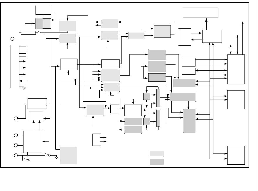
This chapter describes the functional blocks shown in Figure 2-1. Overall descriptions are broken down into Power Supply, Analog Circuitry, and Digital Circuitry.
For all measurements, inputs (e.g., Ëand â) are applied through overvoltage (and overcurrent) protection circuits, switched to an appropriate range, and branched into two signal paths. One path leads first to a Fast A/D Converter (8-bit, 4.8-MHz sample rate) that digitizes the data, then to a digital gate array that stores and processes the data. The other path leads to a Slow A/D Converter (high accuracy, dual slope) in the U30 custom IC. The microprocessor takes data from both the Slow A/D Converter (U30) and the custom digital IC (U24) storage to simultaneously display a waveform and a 4-1/2 digit meter reading. Power supplies include 5.2V dc and -5.2V dc for analog circuitry, 3.3V dc for digital circuits, and VEE (nominally -23V dc) for the LCD module.
Start-Up Sequence |
2-2. |
The GMM sequences through the following steps when power is applied:
•The 3.3V power supply comes up.
•The reset pin on the microprocessor (U25-1) goes high.
•The microprocessor (U25) begins executing the program stored in EEPROMs U11 and U19.
•LCD controller (U13) data is initialized.
•VEE is turned on (-20V dc), and the display comes on.
Function Selection |
2-3. |
When the selector is turned to a new function, a rotary switch wiper sets up a resistor divider by grounding the selected resistor in series with R170. The resulting voltage is read by the microprocessor (U25-83).
2-3

867B,863
Service Manual
Power Supply |
2-4. |
The GMM can be powered with a Fluke BP7217 rechargeable battery pack (6 - 4/3A NiCd cells), 6 AA alkaline batteries, or a battery eliminator. The GMM automatically detects power by source (NiCd battery pack, AA alkaline batteries, or battery eliminator.) Diodes provide reverse polarity protection for the batteries.
The NiCd battery pack recharges in a minimum of 16 hours when the GMM is not operating or at a trickle rate while the GMM is operating. Only cells in the Fluke BP7217 battery pack can be charged internally. Internal charging is not available with Model 863.
|
|
Caution |
|
|
Do not attempt to place other batteries in the BP7217 battery |
||||
pack; damage to the batteries could result. |
|
|||
A low battery indicator ( |
|
) comes on when battery voltage drops below a preset |
||
+ |
||||
voltage level. This level is the same for all types of batteries: remaining battery life can |
||||
vary from minutes to hours, depending on battery type, ambient temperature, and battery |
||||
history. A low-battery power down can also occur. (No automatic power down occurs |
||||
when the GMM is powered by the battery eliminator.) |
|
|||
Refer to Chapter 1 for battery and battery eliminator specifications. |
||||
Power Supply Input Voltages |
|
2-5. |
||
Refer to Table 2-1. |
|
|
||
|
Table 2-1. Power Supply Inputs |
|
||
|
|
|
|
|
Input Source |
Voltage |
Lifetime (w/o Backlight) |
||
|
|
|
|
|
Line |
12 ±5% volts |
-- |
||
|
|
|
|
|
NiCd Battery Pack (Fluke BP7217) |
6-10 volts |
867B : ≥ 8 hrs typical |
||
|
|
|
863: ≥ 10 hrs typical |
|
Alkaline (6-AA) |
5.5-10 volts |
≥ 8 hrs typical |
||
|
|
|
|
|
2-4
|
|
|
U11 |
SWCrtl10 |
|
|
|
|
|
|
LCD Module - Drivers, |
|
||
|
|
|
10Bit DAC |
|
|
|
|
|
|
LCD |
||||
|
|
|
|
|
|
SWCtrl3 |
|
|
|
|
|
240 x200, Backlight |
Contrast |
|
|
|
|
Component |
|
SWControl |
|
To/From uProcessor |
|
|
|
Adjust |
|||
|
DACData |
Ohms/ |
UART |
|
|
|
|
|
|
|
||||
|
Test Source |
|
|
|
|
|
|
|
||||||
|
|
|
Capacitance |
ADControl |
|
ADControl |
|
|
|
|
|
To/From |
||
|
|
|
|
|
Source |
|
|
|
4 1/2 Digit |
|
|
|
||
|
Volts/ohms |
Protection |
|
|
|
DC Filter |
Multiplexer |
|
A/D |
U21 |
|
U13 |
RS-232 |
|
|
|
|
|
|
DC Input |
|
|
|
SRAM |
LCD Controller |
|
|||
|
|
|
|
|
|
|
|
|
|
32 x 8 |
To/From |
|||
|
|
|
|
|
Attenuation |
|
|
|
|
|
1335 |
|||
|
|
|
|
|
|
|
|
|
|
Dsiplay |
||||
|
|
5.2 volts |
|
|
|
|
|
|
|
|
RIC |
|||
|
|
|
|
|
|
|
|
|
|
|
|
|
||
|
|
-5.2 volts |
|
SWCrtl0 |
|
SWCrtl1 |
|
|
|
|
|
|
|
|
|
|
3.27 volts |
|
|
|
|
2 Frequency |
|
|
|
|
|||
|
|
LCD Voltage VEE |
|
|
|
|
|
|
Counters |
|
|
I/O |
|
|
Block.1-2Figure |
SupplyPower |
|
BATTELIM |
|
AC Input |
DC Level |
Circuitry |
|
|
(25 bits) |
Keyboard |
U25 MICROPROCESSOR H8 |
||
|
|
|
|
|
INT1 |
|||||||||
|
|
|
|
|
U3 RMS |
|
|
|
|
|||||
|
|
|
To uProcessor A/D |
Attenuation |
|
|
|
Reference |
Module |
|
||||
|
|
|
BATTTYPE |
|
Converter |
CLK |
|
|
|
|||||
|
|
|
& x10 gain |
|
|
Counter |
|
|
I/O |
|
||||
|
|
|
To uProcessor A/D |
|
|
|
|
(25 bits) |
EEPROM |
|
||||
|
|
|
|
|
|
|
|
|
|
|||||
|
|
|
BATTLVL |
|
|
DACL1 |
Dual |
|
|
|
|
|
||
|
|
|
|
|
|
|
Divide by |
|
|
|
|
|||
|
|
|
To uProcessor A/D |
ACR1-4 |
Comparators |
|
|
|
|
|
|
|||
|
|
|
DACL2 |
|
|
|
|
|
|
|||||
|
|
|
POWER_DOWN* |
|
|
Circuitry |
|
|
Data |
|
||||
|
|
|
|
|
|
|
|
Status and |
|
|||||
|
|
|
From uProcessor |
|
|
|
|
|
|
|
|
|||
|
|
|
|
|
|
|
Trigger |
|
|
|
Control Regs |
Addr |
|
|
|
|
|
|
|
|
|
|
|
|
|
|
|
||
|
|
|
|
|
|
|
|
|
|
|
|
|
|
|
Diagram |
|
|
Attenuation |
|
(Comp.Test |
SWCrtl13 |
Min |
Compare |
Acquisition Cnt. |
|
U11, U19 |
|||
|
|
|
DAC) |
|
||||||||||
|
|
|
|
|
|
|
4.8 MHz |
|
(Trigger) Circuit |
|
||||
|
|
|
Logic Activity/ |
|
|
|
|
|
|
ROM |
||||
|
|
|
|
|
|
|
|
|
|
|||||
|
|
|
|
|
|
|
|
|
|
|
|
2 128 x 8 |
||
|
|
|
External Trigger |
|
Combination/ |
|
|
|
|
|
|
|
||
|
Logic Activity/ |
|
|
|
Filter |
U10 |
|
|
|
|
|
|
||
|
External |
|
|
|
x1/10,x1,x10 |
|
Flash A/D |
|
|
Addr |
|
|
|
|
|
Trigger |
|
Multiplexer |
|
Circuit |
DACL1 |
8 bit/10 Mhz |
Max |
Compare |
Data |
512 x 8 |
|
|
|
|
|
|
|
|
DAC1 |
|
|
|||||||
|
|
|
|
|
|
|
|
|
Acq. |
|
|
|||
|
|
|
|
IR1 |
|
|
|
|
|
|
|
Ram |
|
|
|
|
|
uA |
mA/A |
|
SWCtrl6 |
DACL2 |
DAC2 |
|
|
|
|
|
|
|
mA/uA |
|
|
|
|
|
|
|
|
|
|
|
||
|
|
|
Current |
SHUNTS |
|
Rotary |
Wakeup* to Power Supply |
|
|
|
|
|
|
|
|
AMPS |
|
|
Switch |
|
|
|
|
|
|
||||
|
|
Switching |
|
|
To uProcessor A/D |
|
|
|
|
|
|
|||
|
|
|
|
|
|
|
|
|
|
|
|
|
|
|
|
COM |
|
|
|
Component |
|
|
|
|
|
|
|
|
U20 |
|
|
|
|
|
Test |
|
|
|
|
RIC Function Blocks - U30 |
|
SRAM |
||
|
|
|
Volts/Ohms/Current |
Current to |
|
|
|
|
|
|
|
|
32k x 8 |
|
|
|
Component Test |
|
Voltage |
|
|
|
|
DIC Function Blocks - U24 |
|
System |
|||
|
eps..os2f |
|
|
|
|
|
|
|
||||||
|
|
|
|
|
|
|
|
|
||||||
|
|
|
|
|
|
|
|
|
|
|
|
|
|
|
5-2
2 Operation of Theory
Supply Power

867B,863
Service Manual
Power Supply Output Voltages and Currents |
|
2-6. |
|||||
|
Refer to Table 2-2. |
|
|
|
|
||
|
|
|
Table 2-2. Power Supply Outputs |
|
|||
|
|
|
|
|
|
|
|
Name |
Voltage |
Tol ± V |
Tol ±% |
Ripple |
mA |
Power |
Notes |
|
|
|
|
(peak to |
|
|
|
|
|
|
|
peak) |
|
|
|
VDD |
5.2V |
0.26 |
5.0% |
50 mV rms** |
43 mA |
224 mW |
0.2V p-p maximum noise |
|
|
|
|
|
|
|
to 1 MHz BW |
|
|
|
|
|
|
|
|
VAD |
3.27V |
0.07 |
2.0% |
50 mV rms** |
12 mA |
40 mW |
±0.02%/C max |
|
|
|
|
|
|
|
|
VCC |
3.27V |
0.07 |
2.0% |
50 mV rms** |
82 mA |
271 mW |
VAD and VCC are tied |
|
|
|
|
|
|
|
together, unregulated |
|
|
|
|
|
|
|
DC used for IBL+ |
|
|
|
|
|
|
|
|
VSS |
-5.2V |
0.26 |
5.0% |
50 mV rms** |
32 mA |
166 mW |
0.2V p-p maximum noise |
|
|
|
|
|
|
|
to 1 MHz BW |
|
|
|
|
|
|
|
|
VEE |
-20V |
|
|
na |
5 mA |
115 mW |
TC = -38 mV/°C, center |
|
|
|
|
|
|
|
value adjusted and |
|
|
|
|
|
|
|
stored at test |
|
|
|
|
|
|
|
|
IBL+ * |
4V |
|
±15% |
na |
80 mA |
264 mW |
current for backlight |
|
|
|
|
|
|
|
LED, ±15% |
|
|
|
|
|
|
|
|
IBL- |
|
|
|
na |
|
|
Current Return for IBL+, |
|
|
|
|
|
|
|
max 1.5V burden voltage |
|
|
|
|
|
|
|
|
* IBL is controlled by a linear current source taken from unregulated DC. |
|
||||||
** Measured with an 8842A in AC rms mode. |
|
|
|
||||
2-6
|
|
|
Theory of Operation |
2 |
|
|
|
|
Power Supply |
||
|
Power Supply Signals |
2-7. |
|
||
|
|
Table 2-3. Power Supply Signals |
|
||
|
|
|
|
|
|
|
Signal Name |
Description |
|
|
|
|
|
|
|
|
|
|
BACKLIGHT_ON* |
Control signal generated by U25. In Model 867B, this signal toggles the backlight |
|
|
|
|
|
power levels. |
|
|
|
|
|
|
|
|
|
|
BATT_LVL |
Monitors an attenuated (0 to 5V) version of the raw battery voltage. This signal is |
|
|
|
|
|
monitored by the U25 microprocessor A/D Converter. The attenuation factor is |
|
|
|
|
|
0.0909:1 with an output impedance of approximately 91 kΩ. |
|
|
|
|
|
|
|
|
|
|
BATT_TYPE |
Monitors an attenuation level of the battery charging voltage. The attenuation ratio is |
|
|
|
|
|
0.0901:1 with an output impedance of approximately 91 kΩ. If the measured voltage |
|
|
|
|
|
is greater than 11 volts, the battery is assumed to be an alkaline cell. Voltages 10.5 |
|
|
|
|
|
volts and below indicate that a Fluke BP7217 battery pack has been installed. |
|
|
|
|
|
|
|
|
|
|
BATT_ELIM |
This is a contact on the battery eliminator input receptacle. It is pulled to LINE with 5 |
|
|
|
|
|
kΩ and tied to GND4 through 475Ω, forming a 10.51:1 divider. If open (voltage |
|
|
|
|
|
>1.0V), a line-powered battery eliminator has been installed. If closed (shorted to |
|
|
|
|
|
ground), the battery eliminator is not plugged-in or is not powered. |
|
|
|
|
|
|
|
|
|
|
CONTRAST |
PWM signal from U25. The frequency is set at U25_SYSCLK/(CLOCK_DIVIDER x |
|
|
|
|
|
COUNTER_LIMIT), yielding 4.8 MHz/(4 x 4096), equaling 293 Hz. The PWM signal |
|
|
|
|
|
has 12-bit resolution, which can vary the duty cycle from 0 to 100%. |
|
|
|
|
|
|
|
|
|
|
IBL+ |
Current source generated by power supply used to run the LCD backlight. Current |
|
|
|
|
|
source is controlled by the BACKLIGHT_ON* control signal. Typical current level is |
|
|
|
|
|
80 mA. This is the sourcing node derived from unregulated DC, typically +6.0V |
|
|
|
|
|
(5.8V minimum.) |
|
|
|
|
|
|
|
|
|
|
IBL- |
Current return for IBL+, with approximately 1V burden. |
|
|
|
|
|
|
|
|
|
|
POWER_DOWN |
Powers down the GMM. Signal is generated by U25. This signal shuts the GMM off |
|
|
|
|
|
completely. Pulled-down to GND with 20 |
kΩ. |
|
|
|
|
|
|
|
|
|
PWR_RESET* |
Signal generated by the power supply when the VCC power supply drops below 3.0 |
|
|
|
|
|
volts. The reset lasts 100 milliseconds minimum. If the selector is left in the OFF |
|
|
|
|
|
position or the GMM is powered down, the PWR-RESET* signal restarts the 100 ms |
|
|
|
|
|
time-out period. This signal is pulled up to VCC by 10 kΩ . |
|
|
|
|
|
|
|
|
|
|
VEE_ON |
Control signal generated by U25. Turns the VEE power supply on and off. Pulled |
|
|
|
|
|
down to ground by 100 kΩ . |
|
|
|
|
|
|
|
|
|
|
WAKEUP* |
This signal is generated by both the rotary selector switch and the WAKEUP button. |
|
|
|
|
|
Upon going LOW, followed by a return to HIGH, the GMM powers up. In the OFF |
|
|
|
|
|
position, this feature is overridden by the OFF switch. |
|
|
|
|
|
|
|
|
|
2-7

867B,863
Service Manual
Power ON/OFF Requirements |
2-8. |
The GMM is turned off when the selector is rotated to OFF. If the selector is immediately rotated beyond OFF, the GMM does not turn off. If the selector remains in OFF for 125 ms, GMM software recognizes a valid OFF signal. If the selector remains in the OFF position for more than 250 ms and an OFF signal is not generated, a hardware timeout occurs and the GMM powers off.
The signal PWR_RESET* goes true (LOW) immediately when a software OFF signal or hardware timeout is generated. This action forces a complete restart sequence, with PWR_RESET* remaining low for at least 100 ms.
After a software OFF signal has occurred, turn the GMM on by rotating the selector to any function or by pressing 9(the WAKEUP button.). If a hardware timeout has occurred, pressing 9does not turn the GMM on; the selector must be rotated to a new function.
NiCd Charging Requirements |
2-9. |
Models 867B use an internal two-state charger. The initial charge state is at approximately 170 mA (±30 mA) to allow for full overnight charging (16 hours minimum). The second charge state is at approximately 40 mA (±15 mA) to allow for battery charge maintenance without full charging from a discharged condition.
A timer (reset each time the battery eliminator is plugged in) controls the charge state. The rate shifts to 40 mA after approximately 16 hours of accumulated charge time.
The 40-mA rate is used with batteries below approximately 6 volts to limit the amount of power dissipated when a completely dead battery pack is used. After this 6-volt cutoff point has been reached, the GMM starts charging at 170 mA.
Battery and Line Level Detection |
2-10. |
The BATT_LVL signal is an attenuated version of the battery and charging voltages. Table 2-4 summarizes the values to be used by the software to control LOW BATTERY detection and SOFT SHUTDOWN. After LOW BATTERY is detected, the backlight is turned off and backlight control is disabled.
2-8
|
|
|
|
|
Theory of Operation |
2 |
||
|
|
|
|
|
Power Supply Functional Blocks |
|||
|
|
Table 2-4. Power Source Detection |
|
|
|
|
||
|
|
|
|
|
|
|
|
|
|
POWER TYPE |
DETECTION |
|
LOW BATTERY |
SOFT POWER- |
SCALE |
|
|
|
|
|
OFF |
FACTOR |
|
|
||
|
|
|
|
|
|
|
||
|
Battery Eliminator connected |
BATT_ELIM |
|
na |
na |
0.0951 |
|
|
|
|
≥ 1.0 Volts |
|
|
|
|
|
|
|
|
|
|
|
|
|
|
|
|
NiCd Battery Pack installed |
BATT_TYPE |
|
6.2V |
5.7V |
0.0909 |
|
|
|
|
5 ≤ V ≤10.5 Volts |
|
|
|
|
|
|
|
|
|
|
|
|
|
|
|
|
Alkaline (AA) Batteries installed |
BATT_TYPE |
|
6.2V |
4.8V |
0.0909 |
|
|
|
|
V ≤ 4.5 or |
|
|
|
|
|
|
|
|
V ≥ 11 Volts |
|
|
|
|
|
|
|
|
|
|
|
|
|
|
|
Power Supply Functional Blocks |
|
|
2-11. |
|
||||
Refer to the Schematic Diagram in Chapter 7 during the following discussion. The power supply consists of the circuit blocks listed below. Each block is identified with a letter (A-J) keyed to Figure 2-2.
•Input power selector (A)
•Boost Preregulator (B)
•NiCd battery charger and timeout (C)
•DC-DC Converter (D)
•Backlight current sink (E)
•Power switch, wake-up and power down circuitry (F)
•LCD contrast control and temperature compensator (G)
•Power on reset (H)
•Linear post-regulators (I)
•+5 volt bias supply (J)
Input Power Selector (A) |
2-12. |
The input power selector automatically selects either battery eliminator power (line) or battery. If a battery eliminator is connected to the GMM, +12 volts (±5%) is applied through line filter FL1 to the anode of CR21. This 12 volts turns on Q13, which pulls down the gate of Q14, turning it on. Current can then flow from the battery eliminator to the boost circuit (B). Note that CR22 is back-biased.
If an eliminator is not connected, Q13 is off. Current is not allowed to flow through Q14 until Q12 is turned on. Q12 is turned on when enough voltage remains on the battery to supply the bias regulator (J) and the power wake-up circuitry is enabled. When the GMM is off (with no eliminator connected), Q14 is off and only the bias supply draws current. The maximum off-state current draw is 100 A.
CR21 and CR22 perform the power selection process.
2-9

867B,863
Service Manual
Boost Preregulator (B) |
2-13. |
The boost preregulator outputs +15 volts from an input of +12 volts from the battery eliminator or 5.5 to 10 volts from the battery.
U27 provides this boost in conjunction with L1, CR20, and C3. If U27 is not functioning, the voltage at the positive of C3 is approximately 0.4 volts below the voltage on C90. R114 provides peak current limiting to prevent rapid burnout of the boost circuit in the event of an overload. Since R114 requires a functional U27, it does not provide complete protection. R12 and R73 set the output voltage, while the other discrete components provide timing and compensation for the regulator.
The output of this stage is delivered to the NiCd battery charger (C) and to the DC-DC converter (D). R125 allows the charger and boost circuit to be tested independently of the rest of the GMM. R125 is especially useful if a large load causes <15 volts at the cathode of CR20.
Battery Charger (C) |
2-14. |
The battery charger consists of the following two sections:
•Q22 and its associated components provide a linear current source of either 170 mA or 40 mA to charge the NiCd battery. Transistors Q1, Q2, Q3, Q6, and Q11 provide logic control of the charger state.
•The other part of the circuit is U32 and its associated components, which provide a timeout of at least 16 hours to prevent continuous overcharging of the battery. This circuit is reset each time a battery eliminator is plugged in (via U34, R141, R140 and C91).
A full charge of approximately 170 mA can only be provided to the battery if Q1, Q2, and Q6 are turned on, Q3 is off, and Q11 is off. These states correspond to the GMM being connected to line but turned off and U32 not being timed out. U32 is inhibited from advancing by CR5 when power is on.
VR1 prevents Q2 from turning on until the battery voltage rises above about 5.8 volts. This prevents excessive power dissipation in Q22 with a dead battery or shorted cells.
Note
The Fluke battery pack (BP7217) uses an extra wire to allow charging current to flow. If individual batteries are installed, no connection is made, and no charging current can flow.
2-10

|
|
|
FL1 |
|
LINE |
CR21 |
|
|
|
|
|
|
|
|
|
|
A |
|
|
|
|
B |
|
|
|
|
|
|
|
|
CR20 |
|
|
|
|
|
|
|
|
|
|
|
|
|
|
|
|
|
|
|
|
|
|
|
|
|
|
|
|
|||
|
|
|
|
|
1N5817 |
|
|
|
|
|
|
|
|
|
|
|
|
|
|
|
|
|
|
|
|
L1 |
1N5817 |
R125 |
|
|
|
|
|
|
|
|
|
|
|
|
|
|
|
|
|
|
|
|
|
|
|
|
|
|
|
|||||||
P3 |
B |
B |
CB |
CB |
|
|
|
|
|
|
|
|
|
|
|
|
|
|
|
|
|
|
|
|
|
|
1 |
2 |
|
|
|
|
|
|
E |
|
|
|
|
|
|
|
|
|
|
|
|
|
|
|
|
|
|
|
|
|||||||
1 |
PSG |
|
|
CG1 |
|
|
|
|
1 |
2 |
3 |
|
5 |
6 |
7 |
8 |
|
|
|
|
|
|
|
R12 |
|
|
|
|
|
330UH |
|
0 |
|
|
|
|
|
|
|
|
|
|
|
|
|
|
|
|
|
|
|
|
|
|
|
|
|
|||||
P3 |
|
GND |
C60 |
|
|
|
|
|
|
|
|
|
|
|
|
C90 |
|
|
|
|
|
|
|
|
|
|
|
|
|
|
|
|
|
|
|
|
|
|
|
|
|
|
|
|
|
|
|
|
|
|
|
|
|
|
|
|
||||||
2 |
|
|
|
|
|
|
|
|
|
|
|
|
|
|
|
|
|
|
|
|
|
140.0K |
|
|
|
|
|
|
|
|
|
|
|
|
|
|
|
|
|
|
|
|
|
|
|
|
|
|
|
|
|
|
|
|
|
|
||||||
P3 |
|
|
|
|
|
10UF |
|
|
|
|
|
|
|
Q14 |
|
|
|
220UF |
|
|
|
|
|
|
|
|
|
|
|
|
|
|
|
|
|
|
|
|
|
|
BACKLIGHT |
|
|
|
|
|
|
|
|
|
|
|
|
|
|
|||||||
3 |
|
|
|
|
|
35V |
|
|
R137 |
|
|
|
SI9430DY |
|
25V |
|
|
|
|
|
|
|
|
|
|
|
|
|
|
|
|
|
|
|
|
|
|
|
|
|
|
|
|
|
|
|
|
|
|
|
|
|
|
|
||||||||
|
|
|
|
|
|
|
|
|
|
|
4 |
|
20% |
|
|
|
|
|
|
|
|
|
|
|
|
|
|
C3 |
|
|
|
|
|
|
|
|
|
|
|
|
|
|
|
|
|
|
|
|
|
|
|
|
|
|
|
|
||||||
|
|
|
|
|
|
|
|
|
100K |
|
|
|
|
|
|
|
D |
|
|
|
|
|
|
|
|
8 |
|
|
|
|
|
|
|
|
|
|
|
|
CURRENT SINK |
|
|
|
|
|
|
|
|
|
|
|
|
|
|
|||||||||
|
|
|
D |
|
D |
|
|
|
|
|
|
|
|
|
|
|
|
|
|
|
C59 |
|
|
|
|
|
|
220UF |
|
|
|
|
|
|
|
|
VDD |
|
|
|
|
|
|
|
|
|
|
|
|
|
|
|||||||||||
|
|
|
|
|
|
|
|
|
|
|
|
|
|
|
|
|
|
|
|
|
|
|
|
|
|
VS |
|
|
|
|
|
|
|
|
|
|
|
|
|
|
|
|
|
|
|
|
|
|
|
|
||||||||||||
|
|
|
|
|
|
|
CR22 |
|
|
|
|
|
|
|
|
|
|
|
|
|
|
|
R122 |
2200PF |
1 |
INM |
|
|
COL |
|
6 |
20% |
|
|
|
|
|
|
|
|
|
|
|
|
|
|
|
|
|
|
|
|
|
|
|
|
|
|
|
|
||
|
|
|
|
|
|
|
1N5817 |
|
10K |
|
|
|
|
|
|
10K |
|
|
|
|
221K |
CER |
|
2 |
INP |
|
|
EMIT |
|
5 |
D |
|
|
|
|
|
|
|
|
|
|
|
80 MA |
|
|
|
|
|
|
|
|
|
|
|
|
|
|
|
|
|||
|
|
|
|
|
|
|
|
|
|
|
|
|
|
|
|
|
POK-1 |
|
|
|
3 |
|
|
|
|
|
7 |
|
|
|
|
|
|
|
|
|
|
R106 |
|
|
|
|
|
|
|
|
|
|
|
|
|
|
|
|
|
|
||||||
|
|
|
|
|
|
|
|
|
|
|
|
|
|
|
|
|
|
|
|
|
|
C23 |
|
|
OSC |
GND CLIM |
|
|
|
|
|
|
|
|
|
|
|
|
|
|
|
|
|
|
|
|
|
|
|
|
IBL- |
|
|
|
|
|||||||
|
|
|
|
|
|
|
|
|
|
|
|
|
Q13 |
|
|
|
|
Q12 |
R73 |
|
C56 |
|
|
|
|
U27 |
|
|
|
|
|
|
|
|
|
|
3.24K |
|
|
|
|
|
|
|
|
|
|
|
|
|
|
|
|
|
||||||||
|
|
|
|
|
|
|
|
|
|
|
|
|
|
|
|
|
22PF |
|
|
4 |
|
R114 |
|
|
|
|
|
|
|
|
|
|
|
|
|
|
|
|
|
|
|
|
|
|
|
|
|
|
|
|
||||||||||||
|
|
|
|
|
|
|
|
|
|
|
|
MUN2211 |
|
|
|
MUN2211 |
10.0K |
|
CER |
|
680PF |
|
|
|
LM3578AN |
0.2 |
|
|
|
|
|
|
|
|
|
|
|
Q21 |
|
|
|
|
|
|
|
|
|
|
|
|
|
|
|
|
||||||||
|
|
|
R7 |
|
|
|
|
|
|
|
|
|
|
|
|
|
CER |
|
|
D |
|
|
|
|
|
|
|
|
|
|
|
|
R158 |
|
|
|
|
|
|
|
|
|
IBL+ |
|
|
|
|
|||||||||||||||
|
|
|
|
|
|
|
|
|
|
|
|
|
|
|
|
|
|
|
|
|
|
|
|
|
|
|
|
|
|
|
|
|
|
|
|
|
|
|
|
|
|
|
|
4401 |
|
|
|
|
|
|
|
|
|
|
|
|
|
|
||||
|
|
|
4.99K |
|
|
|
|
|
|
|
D |
|
|
|
|
|
D |
|
|
|
|
|
|
|
|
|
|
|
|
|
|
|
|
|
|
|
|
|
|
|
|
|
|
|
|
|
47 |
|
|
|
|
|
|
|
|
|
|
|
|
|
|
|
|
|
|
BATT_ELIM |
+15 |
|
|
|
|
|
|
|
|
|
|
|
|
|
|
|
|
D |
|
D |
|
|
|
|
|
|
|
|
|
|
|
|
|
Q5 |
|
|
|
|
|
|
|
|
(867B only) |
|
|
|
|
|
|
|
|
|
|
|
|
|
|
||
|
|
|
|
|
|
|
|
|
|
|
|
|
|
|
|
|
|
|
|
|
|
|
|
|
|
|
|
D |
|
|
|
|
MUN2211 |
10K |
|
R11 |
|
|
|
D |
|
|
|
|
|
|
|
|
|
|
|
|
|
|
||||||||
R6 |
|
|
|
|
|
|
|
|
|
|
|
|
|
|
|
|
|
|
|
|
|
|
|
|
|
|
|
U15 |
|
|
|
|
|
|
|
|
|
|
|
|
|
|
3.24K |
|
R16 |
|
|
|
|
|
|
|
|
|
|
|
|
|
|
|
|
|
475 |
|
|
|
|
|
|
|
|
|
|
|
|
|
|
|
|
|
|
|
|
|
|
|
|
CR8 |
|
|
|
|
|
|
|
|
|
|
|
|
|
|
|
|
|
|
|
|
|
|
|
|
|
|
|
|
|
|
|
|
|
||||
|
|
|
|
|
|
|
|
|
|
|
|
|
|
|
|
|
|
|
|
|
|
|
|
|
LM2936M |
|
|
|
|
|
|
|
|
|
|
|
|
|
|
10 |
|
|
|
|
|
|
|
|
|
|
|
|
|
|
|
|
||||||
|
|
|
|
|
|
|
|
|
|
|
|
|
|
|
|
|
|
|
|
|
|
|
|
|
MMBD7000 |
|
|
|
|
|
|
|
|
|
|
|
|
|
|
0.2 (867B only) |
|
|
|
|
|
|
|
|
|
|
|
|
|
|
||||||||
|
|
|
|
|
|
|
|
|
|
|
|
|
|
|
|
|
|
|
|
|
|
|
|
|
|
|
|
|
|
|
+5B |
|
|
|
|
|
|
|
|
|
|
|
|
|
|
|
|
|
|
|
|
|
|
|
|
|
||||||
|
|
|
|
|
R74 |
|
|
|
|
|
|
|
|
|
|
|
|
|
|
|
|
|
|
|
|
|
8 |
IN |
|
OUT |
1 |
|
|
|
|
|
|
|
|
D |
D |
|
|
|
|
|
|
|
|
|
|
|
|
|
|
|
|
|
|
|
||
|
D |
|
|
|
|
R113 |
|
|
|
|
|
|
|
|
|
|
|
|
|
|
|
|
|
|
|
|
|
|
|
|
|
C85 |
|
|
|
|
|
|
|
|
|
|
|
D |
|
|
|
|
|
|
|
|
|
|
|
|
|
|
|
|
||
|
|
|
|
1.82K |
|
|
|
|
|
|
|
|
|
|
|
|
|
|
|
|
|
|
|
|
|
GND |
|
|
|
|
|
|
|
|
|
|
|
|
|
|
|
|
|
|
|
|
|
|
|
|
|
|
|
|
|
|
||||||
|
|
|
|
|
|
|
12.1 |
|
|
|
|
|
|
|
|
|
|
|
R14 |
|
|
|
|
|
|
|
|
|
|
10UF |
J |
|
|
|
|
|
|
|
|
|
|
|
|
|
|
|
|
|
|
|
|
|
|
|
|
|
|
|
||||
|
|
|
|
|
|
|
|
|
|
|
|
|
|
|
|
|
|
|
|
|
|
|
|
4 |
|
|
|
|
|
|
16V |
|
|
|
|
|
|
|
|
|
|
|
|
|
|
|
|
|
|
|
|
|
|
|
|
|
|
|
||||
|
CR9 |
|
|
|
|
1/2W |
|
|
|
|
|
|
|
|
|
|
|
1.00MEG |
|
|
|
|
|
2 |
3 |
6 |
7 |
|
|
|
|
|
|
|
|
|
|
|
|
|
|
|
|
|
|
|
|
|
|
|
|
|
|
|
|
|||||||
|
|
|
|
|
10% |
|
|
|
|
|
|
|
|
|
|
|
|
|
|
|
|
|
|
|
|
|
|
|
|
|
20% |
|
|
|
|
|
|
|
|
|
|
|
|
|
|
|
|
|
|
|
|
|
|
BACKLIGHT_ON* |
|
|
|
|||||
MMBD7000 |
|
|
|
|
|
|
|
|
|
|
|
R56 |
|
|
|
|
|
|
|
|
|
|
|
|
|
|
|
|
|
|
|
|
|
|
|
|
|
|
|
|
|
|
|
|
|
|
|
|
|
|
|
|
|
|
|
|||||||
|
|
|
|
|
|
|
Q22 |
|
|
|
|
|
|
|
|
|
|
|
|
|
|
|
|
|
D |
|
|
|
|
|
|
|
|
|
|
|
|
|
H |
|
|
INT_VCC |
|
|
|
|
|
|
|
|
|
|
|
|
|
|
||||||
|
|
|
|
|
|
|
|
|
|
|
|
|
1.00MEG |
|
|
|
|
|
|
|
|
|
|
|
|
|
|
|
|
|
|
|
|
|
|
|
|
|
|
|
|
|
|
|
|
|
|
|
|
|
|
|
|
|
|
|
||||||
Figure |
|
|
|
|
|
|
MJD32 |
|
|
|
|
|
|
|
|
|
|
|
|
|
|
|
|
|
|
|
|
|
|
|
BATT_TYPE |
|
|
|
|
|
|
|
|
|
|
|
|
|
|
|
|
|
|
|
|
|
|
|
|
|
|
|
||||
|
|
|
MUN2211 |
|
|
|
|
|
|
|
|
|
|
|
|
D |
|
|
|
|
C |
|
|
|
|
|
|
|
|
|
|
|
|
|
|
|
|
|
|
|
|
|
|
|
|
|
|
|
|
|
|
|
|
|
|
|
||||||
|
|
|
R55 |
|
|
BT1 |
|
|
|
|
|
|
|
|
|
|
|
|
|
|
|
|
|
|
BATT_LVL |
|
|
|
|
|
|
|
|
|
|
|
|
3 |
|
|
|
|
|
|
|
|
|
|
|
|
|
|
|
|
||||||||
|
|
|
|
|
|
|
|
|
|
|
|
R29 |
|
|
|
|
|
|
|
|
|
|
|
|
|
|
|
|
|
|
|
|
|
|
|
|
|
|
|
|
|
|
|
|
|
|
|
|
|
|
|
|
|
|
|
|
|
|
|
|||
|
|
|
R100 |
|
6.49K |
|
|
6- 4/ 3A |
|
|
|
|
|
|
|
|
|
|
|
|
|
|
|
|
|
|
|
|
|
|
|
|
|
|
|
|
|
|
|
|
R69 |
|
|
|
R124 |
|
|
|
|
|
|
|
|
|
|
|
|
|
|
|||
|
|
|
|
|
|
|
|
|
|
|
|
100K |
|
|
|
|
|
|
|
|
|
|
|
|
|
|
|
|
|
|
|
|
|
|
|
|
|
|
|
|
|
|
|
|
|
|
|
|
|
|
|
|
|
|
|
|
||||||
|
|
|
24.9K |
|
|
VR1 |
|
|
|
|
|
|
|
|
R27 |
|
|
|
|
|
|
|
|
|
|
|
|
|
|
|
|
|
|
|
|
|
|
|
|
6.34K |
|
|
|
3.32M |
|
|
R115 |
|
|
|
|
|
|
|
|
|
|
|
||||
|
|
|
|
|
|
|
|
|
|
M4 |
|
|
|
|
|
|
100K |
|
|
|
|
|
|
|
|
|
|
|
|
|
|
|
|
|
|
|
|
|
|
|
|
|
|
|
|
|
|
10.0K |
|
|
|
|
|
|
|
|
|
|
|
|||
|
|
|
|
|
|
|
5231B |
|
|
|
|
|
|
|
|
|
|
|
|
|
|
|
|
|
|
|
|
|
|
|
|
|
|
|
|
|
|
|
|
|
|
|
|
|
|
|
|
|
|
|
|
|
|
|
|
|
|
|
||||
|
|
|
|
|
|
|
|
|
|
|
|
|
|
|
|
|
|
|
|
|
|
|
|
|
|
|
|
|
|
|
|
|
|
|
|
|
|
|
|
|
|
|
|
|
|
|
LM393DT |
|
|
|
|
|
|
|
|
|
|
|
|
|
|
|
|
|
|
|
|
Q2 |
10K |
LINE |
|
|
|
|
|
|
D |
|
|
|
|
|
|
|
|
|
|
|
|
|
|
|
|
|
|
|
|
|
|
|
|
|
|
|
|
|
|
|
|
|
|
|
|
|
|
|
|
|
|
|
|
|
|
|
|
|
|
|
|
|
|
|
|
|
|
|
|
|
|
|
|
|
|
|
|
|
|
|
|
|
|
|
|
|
|
|
|
|
|
|
|
|
|
|
|
|
|
|
8 |
U22 |
|
|
|
|
|
|
|
|
|
|
|
|
|
|
||||
|
|
|
|
|
|
|
|
|
|
|
|
|
|
|
|
|
|
|
|
|
|
|
|
|
|
|
|
|
|
|
|
|
|
|
|
|
|
|
|
|
|
|
|
|
|
|
|
|
|
|
|
|
|
|
|
PWR_RESET* |
|
|
|
|||
-2 |
|
|
|
|
|
R15 |
|
|
|
D |
|
|
|
|
|
|
|
|
|
|
|
|
|
|
|
|
|
|
|
|
|
|
|
|
|
|
|
|
LM4040-2.5 |
|
+2.5V |
|
|
|
2 |
|
1 |
|
|
|
|
|
|
|
|
|
|
|
|
|||
|
|
|
|
|
|
|
|
|
|
|
|
|
|
|
|
|
|
|
|
|
|
|
|
|
|
|
|
|
|
|
|
|
|
|
|
|
|
|
|
|
|
RES |
|
|
|
|
|
|
|
|
|
|
|
|
|
|
||||||
|
|
|
|
|
|
R28 |
|
|
|
|
|
|
|
|
|
|
|
|
|
|
|
|
|
|
|
|
|
|
|
|
|
|
|
|
|
|
|
|
|
|
|
|
|
|
4 |
|
|
|
|
|
|
|
|
|
|
|
|
|
|
|||
|
|
|
|
|
100K |
|
|
|
|
|
|
|
|
|
|
|
|
|
|
|
|
|
|
|
|
|
|
|
|
|
|
|
|
|
|
|
|
U31 |
|
|
|
|
|
|
|
|
|
8 |
RES |
|
|
|
|
|
|
|
|
|
||||
|
|
|
|
|
|
100K |
|
|
|
|
|
|
|
|
|
|
|
|
|
|
|
|
|
|
|
|
|
|
|
|
|
|
|
|
|
|
|
|
|
|
|
|
|
|
|
|
6 |
|
|
|
|
|
|
|
|
|
||||||
.2 |
|
|
|
|
Q1 |
10K |
|
|
U32 |
|
|
|
|
|
|
|
|
|
|
|
5 |
|
|
|
|
|
|
|
|
|
|
|
|
|
|
|
|
|
|
|
R81 |
|
C19 |
|
|
D |
|
|
5 |
|
7 |
|
|
|
|
|
|
|
|
|
||
|
|
|
MUN2211 |
|
|
7 |
74HC4060DT |
9 |
|
|
|
|
|
|
|
|
|
|
|
|
|
|
|
|
|
|
|
|
|
|
|
|
|
|
|
|
|
|
|
|
|
|
|
U22 |
|
|
|
|
|
|
|
|
|
|||||||||
|
|
|
|
|
|
|
|
Q4 |
CKO |
|
|
|
|
|
|
|
|
|
|
|
|
|
|
|
|
|
|
|
|
|
|
|
|
|
|
R119 |
|
|
31.6K |
|
|
10UF |
|
|
C58 |
|
|
|
4 |
LM393DT |
|
|
|
|
|
|
|
|
|
|||
Power |
|
|
|
|
|
|
|
5 |
|
|
R44 |
|
|
|
|
|
|
|
|
|
|
|
|
|
|
|
|
|
|
|
|
|
|
|
|
|
|
|
16V |
|
|
|
|
|
|
|
|
|
|
|
|
|
|
|||||||||
|
|
|
|
|
|
|
4 |
RESET |
|
|
10 |
|
|
|
|
|
|
|
|
|
|
|
|
|
|
|
|
|
|
|
|
|
|
CR19 |
10UF |
|
|
|
|
20% |
|
R132 |
|
|
1UF |
|
|
|
|
|
|
|
|
|
|
|
||||||
|
|
|
|
|
|
|
|
Q5 |
|
|
|
|
|
|
|
|
|
|
|
|
|
|
|
|
|
|
|
|
|
|
|
|
|
10.0K |
|
|
|
|
|
|
|
0.1UF |
|
|
|
|
|
|
|
|
|
|
|
|
|
|
||||||
|
|
|
|
|
|
|
|
6 |
Q6 |
CKO* |
|
|
464K |
|
|
C84 |
|
|
|
LINE |
|
|
|
|
|
|
|
|
|
|
|
|
|
|
|
|
|
D |
|
|
|
|
|
|
CER |
|
|
|
|
|
|
|
|
|
|
|
|
|
|
|||
|
|
|
|
|
|
|
|
14 |
Q7 |
|
|
|
11 |
|
|
|
|
|
|
|
|
|
|
|
|
|
|
|
|
|
|
|
|
|
|
|
|
|
|
|
|
25V |
|
|
D |
|
|
|
|
|
|
|
|
|
|
|
||||||
|
|
|
|
|
|
10K |
|
13 |
Q8 |
CKI |
|
|
|
|
|
|
|
|
|
|
|
|
|
|
|
|
|
|
|
|
|
|
|
|
|
|
|
|
|
|
|
|
D |
|
|
D |
|
|
|
|
|
|
|
|
|
|
|
|
|
|
|
|
|
|
|
|
|
Q6 |
|
|
15 |
Q10 |
|
|
|
|
|
R68 |
|
10UF |
|
|
|
R141 |
|
|
|
|
|
|
|
|
|
|
|
|
|
|
|
|
|
|
|
|
|
|
|
|
|
|
|
|
|
|
|
|
INT_VCC |
|
|
|
|
|
|||
|
|
|
|
MUN2211 |
|
|
1 |
Q12 |
|
|
|
|
1.00MEG |
|
20% |
|
|
|
|
|
|
|
|
|
|
|
|
|
|
|
|
|
|
|
|
|
|
|
|
|
|
|
|
|
|
|
|
|
|
|
|
|
|
|
|
|||||||
|
|
|
|
|
|
|
|
|
+5B |
|
|
|
|
|
|
100K |
|
|
|
|
|
|
|
|
|
|
|
|
|
|
|
|
|
Q23 |
|
|
|
|
|
|
|
|
|
|
|
|
|
|
|
|
|
|
|
|
||||||||
|
|
|
|
|
|
|
|
2 |
Q13 |
|
|
|
|
|
|
|
16V |
|
|
|
|
|
|
|
|
|
|
|
|
|
|
|
|
|
|
C9 |
|
|
|
|
|
|
|
|
|
|
|
|
|
|
|
|
|
|
|
|
|
|||||
|
|
|
|
|
|
|
|
3 |
Q14 |
|
|
|
|
|
|
|
|
|
AL |
|
|
|
|
|
|
|
|
|
|
|
|
|
|
|
|
|
|
|
|
|
4401 |
|
|
|
|
|
|
|
|
C2 |
|
|
|
|
|
|
|
|
|
|
|
|
|
|
|
|
|
D |
|
|
|
|
|
|
|
|
|
|
|
|
|
U34 |
|
|
|
|
|
|
|
|
|
|
|
|
|
|
|
|
|
|
|
1N5817 |
16V |
|
R72 |
VCCDRIVE |
|
|
|
3.24K |
|
|
20V |
|
|
|
|
|
|
|
|
|
|
|
|
|
|
|
|
|
|
|
|
|
|
|
|
|
|
|
|
|
|
|
|
|
|
|
|
|
|
|
|
|
|
|
|
|
|
|
|
|
20% |
|
|
|
|
|
|
|
|
|
|
|
|
|
|
|
|
|
||||||||
Supply |
|
|
|
|
|
|
|
|
12 |
|
|
|
|
|
|
|
|
|
4 |
|
|
R140 |
|
|
|
|
|
|
|
|
|
|
|
|
|
|
|
475 |
|
|
|
|
|
|
|
|
|
|
|
|
|
|
|
|
|
|
|
|
||||
|
|
|
|
|
|
|
|
|
|
|
|
|
|
|
|
|
6 |
HC132 |
5 |
|
|
66.5K |
|
|
|
|
|
|
|
|
|
|
|
|
|
D |
|
|
7 |
|
6 |
|
|
|
|
|
|
D |
|
|
|
|
|
|
|
|
|
|
|
|||
|
|
|
|
|
|
|
|
|
|
|
|
|
|
|
|
|
|
|
|
|
C91 |
|
|
|
|
|
|
|
|
|
|
|
|
|
|
|
|
|
|
|
5 |
|
|
|
|
|
|
|
|
|
|
|
|
|
|
|
|
|
||||
|
|
|
|
|
|
|
|
|
CR15 |
|
|
|
|
|
|
|
|
|
+5B |
|
|
|
|
|
|
|
|
|
|
|
|
|
|
|
|
CR18 |
|
|
|
U2 |
|
|
|
R128 |
|
|
|
|
|
|
|
|
R52 |
|
|
|
|
|||||
|
|
|
|
|
|
|
|
|
|
|
|
|
|
|
|
|
|
|
|
|
|
|
1UF |
|
|
|
|
|
|
|
|
|
|
|
|
C21 |
1N5817 |
|
|
|
MC33172 |
|
|
|
|
|
|
|
|
|
|
|
|
|
|
|
VDD |
|
|
|
||
|
|
|
|
|
|
|
|
|
|
|
|
|
|
|
|
|
|
|
|
|
|
|
20V |
D |
|
|
|
|
|
|
|
|
|
|
|
1UF |
|
|
|
|
|
|
10.0K |
|
|
|
|
|
|
|
|
0 |
|
+5.2 |
|
|
|
|||||
|
|
|
|
Q3 |
10K |
|
|
|
MMBD7000 |
|
|
|
|
|
|
|
|
|
|
|
|
|
|
|
|
|
|
|
|
|
20V |
|
|
|
|
|
|
|
|
|
|
|
|
C88 |
|
|
INT_VDD |
|
TP4 |
|
R87 |
|
|
|
|
|||||||
|
|
|
|
|
|
|
|
|
|
|
|
|
|
|
D |
|
|
|
|
|
|
|
|
|
|
|
|
|
|
|
|
|
|
|
|
|
|
|
|
|
|
|
|
|
|
|
|
|
||||||||||||||
|
|
|
MUN2211 |
|
|
|
|
|
|
|
|
|
|
|
|
|
|
|
|
|
|
|
|
|
|
|
|
|
|
|
|
|
|
|
|
Q18 |
|
|
|
|
|
|
|
|
|
|
|
|
VAD |
|
|
|
||||||||||
|
|
|
|
|
|
|
|
|
|
|
|
|
|
|
|
|
|
|
|
|
CR5 |
|
|
|
|
|
|
|
|
|
|
|
|
|
|
|
|
|
|
D |
|
1UF |
|
|
|
|
D |
|
|
TP5 |
0 |
|
|
|
||||||||
|
|
|
|
|
|
|
|
|
|
|
|
|
|
|
|
|
|
|
|
|
|
|
|
|
|
|
|
|
|
|
|
|
|
CR12 |
|
|
|
|
|
|
|
|
|
|
|
|
|
|
|
|
|
|
||||||||||
|
|
|
|
|
|
|
|
|
|
|
|
|
|
|
|
|
|
|
|
|
|
|
|
|
|
|
|
|
|
|
|
|
D |
|
|
|
|
|
|
|
4401 |
|
|
20V |
|
|
|
|
|
|
|
|
|
|
|
|||||||
|
|
|
|
|
|
|
|
|
|
|
|
|
|
|
|
|
|
|
|
|
|
|
|
MMBD7000 |
|
|
|
|
|
|
|
|
|
BAV74 |
|
|
|
|
|
|
|
|
|
|
|
|
|
|
|
|
|
|
|
|
|
|
|
|
|
|
||
Blocks |
|
|
|
|
|
|
10K |
|
|
|
|
|
|
|
|
|
|
|
|
|
|
|
|
|
|
|
|
|
|
|
|
|
|
|
35V |
|
|
|
MMBD7000 |
C61 |
|
|
|
|
10.0K 10.7K R19 10.0K |
|
|
Q10 |
|
Q17 |
|
|
C62 |
|
0 |
0 |
|
|
|
|||
|
|
|
|
D |
|
|
|
|
|
|
|
|
|
|
|
|
|
|
|
|
|
|
|
|
|
|
|
|
|
|
|
|
|
|
|
|
|
|
|
4403 |
R133 |
|
|
R123 |
|
5087 |
|
R41 |
|
INT_VSS |
0 |
-5.2 |
+3.3 |
|
||||||||
|
|
|
|
|
|
Q11 |
|
|
|
|
|
|
|
|
|
|
|
|
U34 |
|
|
|
|
|
|
|
|
|
|
|
|
|
|
|
D |
|
|
|
|
|
|
20V |
475 |
|
R89 |
|
|
1.82K |
|
|
|
6429 |
221K |
|
6V |
10.0K |
|
RIC_VCC |
|
|
||
|
|
|
|
|
|
MUN2211 |
|
|
|
|
|
|
|
|
|
|
|
1 |
|
|
|
|
|
|
|
|
|
|
|
|
|
|
|
|
|
|
|
|
|
|
C65 |
|
|
2 |
|
|
|
|
|
R143 |
|
|
R43 |
|
R8 |
|
CONTRAST |
|
|
|
||
|
|
|
|
|
|
|
|
|
|
|
|
|
|
|
|
|
|
2 |
|
|
3 |
|
|
|
POK-1 |
|
|
|
|
|
|
|
|
|
|
|
|
D |
|
1 |
|
|
|
|
|
|
|
100K |
|
|
221K |
|
10.0K |
|
|
|
||||||
|
|
|
|
|
|
|
D |
|
|
|
|
|
|
|
|
|
|
|
|
|
|
|
|
|
|
|
|
|
|
|
|
|
|
|
|
|
|
|
|
|
|
20V |
|
|
3 |
|
|
|
R116 |
|
|
|
|
|
|
|
|
VEE_ON |
|
|
|
|
|
|
|
|
|
|
|
|
|
|
|
|
|
|
|
|
|
|
|
+5B |
|
|
|
|
|
|
|
|
|
|
|
|
|
|
|
|
|
7 |
1 |
|
|
|
|
|
|
U4 |
R39 |
|
5.62K |
|
|
|
|
|
|
|
|
|
|
|
|||
|
M1 |
|
|
|
|
|
|
|
|
|
|
|
|
|
|
|
|
|
|
|
|
|
|
|
|
+5B |
|
|
|
|
|
CR14 |
|
C94 |
Q16 |
|
2 |
|
|
|
|
|
|
MC33172 |
|
|
|
|
|
|
|
|
|
|
TP1 |
|
|
|
|
|
||
|
|
|
|
|
|
|
|
|
|
|
|
|
|
|
|
|
|
|
|
|
|
|
|
|
|
|
|
|
|
|
|
|
|
|
|
|
VDDDRIVE |
|
|
|
|
|
|
|
|
|
|
R48 |
VSS |
|
|
|
||||||||||
|
|
|
|
|
|
|
|
|
|
|
|
|
|
|
|
|
|
|
|
|
|
|
|
|
|
|
|
|
|
|
|
|
BAT54S |
1UF |
SI9955DY |
8 |
3 |
|
|
|
Q19 |
|
|
|
|
|
|
|
|
|
|
|
|
|
|
|
|
|
|
|
||
|
|
|
|
|
|
R126 |
|
|
|
|
|
|
|
|
|
|
|
|
|
|
|
|
|
|
U33 |
|
|
|
|
|
|
|
|
|
|
7 |
|
|
|
|
|
|
|
|
|
|
|
C12 |
|
R142 |
|
|
|
|
|
LCD |
|
|
|
|
|
|
|
|
|
|
|
|
1.00MEG |
|
|
|
|
|
|
|
|
|
|
|
|
|
|
|
R10 |
|
|
|
|
|
|
|
|
|
|
|
1 |
8 |
4 |
D |
|
|
|
|
+REG |
|
D |
|
1UF |
|
|
|
|
|
|
|
|
|
|
|
|||||
|
1 |
|
|
|
|
9 |
U34 |
8 |
R138 |
|
|
CR25 |
|
|
|
|
|
|
|
|
12 |
10 |
Q |
9 |
C57 |
|
|
|
R36 |
R23 |
D |
2 |
9 |
5 |
C63 |
|
|
|
R13 10.0K |
20V |
|
100K |
|
Q20 |
|
|
|
CONTRAST |
|
|
|
|
||||||||||
|
|
|
|
|
|
|
|
|
|
|
|
|
|
10.0K |
|
D PR |
|
|
|
|
|
|
|
|
|
|
|
|
|
|
|
|
|
|
|
|
|
|||||||||||||||||||||||||
|
|
|
|
|
|
10 |
|
|
100K |
|
|
|
|
|
|
|
|
|
|
12 |
U34 |
|
HC74 |
|
|
0.01UF |
|
|
475 |
22.1 |
|
3 |
6 |
|
|
0.22UF |
|
475 |
|
|
|
|
|
|
|
|
|
|
|
|
CONTROL |
|
|
|
|
|
||||||
|
|
|
|
|
|
|
HC132 |
|
|
|
|
|
BAT54 |
|
|
|
|
|
|
|
|
|
|
|
|
|
|
|
|
|
|
|
|
|
5 |
6 |
|
CER |
|
R46 |
|
|
|
|
|
|
|
|
6429 |
|
|
|
|
|
|
|
|
|
||||
D |
TP6 |
5 |
|
3 |
OFF |
S1 |
+5B |
|
|
|
|
|
|
|
C22 |
|
|
HC132 |
11 |
11 |
|
|
|
CER |
|
|
|
|
|
|
|
|
T1 |
|
CR17 |
|
|
|
8 |
6 |
|
|
D |
D |
R120 |
|
|
|
|
|
|
|
G |
|
|
|||||||
MECCA CLIP TP |
|
|
R139 |
|
|
|
|
|
|
|
|
13 |
|
|
+5B |
|
|
C24 |
|
|
|
|
|
|
|
|
|
D |
R94 |
|
|
7 |
|
|
|
|
|
R9 |
59.0K |
|
|
|
|
|
|
|
|
|
||||||||||||||
|
|
|
|
|
|
|
|
|
|
|
|
|
470PF |
|
|
|
|
|
|
|
|
|
|
R17 |
R26 |
|
4 |
RITA-6303 |
|
MMBD7000 |
475 |
|
|
U4 |
|
5 |
|
|
|
|
|
|
INT_VDD |
|
|
|
|
|||||||||||||||
|
|
|
|
|
|
|
|
|
1.00MEG |
|
|
|
|
|
|
CER |
|
|
+5B |
|
|
|
|
8 |
|
|
|
|
|
|
|
|
|
|
|
|
|
|
|
|
|
|
18.7K |
|
|
|
|
|
|
|
||||||||||||
|
|
|
|
|
|
|
|
|
|
|
C10 |
|
1% |
|
|
|
|
|
CL |
Q |
0.01UF |
|
|
475 |
22.1 |
|
|
|
|
|
|
|
|
MC33172 |
4 |
|
|
|
|
|
|
|
8 |
VCCDRIVE |
TP2 |
|
|
|||||||||||||||
|
|
|
|
|
|
D |
|
|
|
|
|
|
|
|
|
|
|
|
|
|
|
|
|
|
|
|
R131 |
D |
|
|
VR2 |
|
|
|
VDDDRIVE |
|
D |
|
|
|
|
INT_VSS |
|
|
3 |
|
|
|
|
|||||||||||||
|
|
|
|
|
|
|
|
|
|
|
|
|
1UF |
|
|
D |
|
|
|
|
|
13 |
|
|
CER |
|
|
|
|
|
|
|
|
|
|
|
|
|
|
|
|
|
|
|
|
|
|
|
|
1 |
VEE |
|
|
|
|
|||||||
|
1000PF |
|
|
|
|
|
|
|
|
|
|
|
|
20V |
R130 |
|
+5B |
|
|
|
|
|
|
|
|
|
|
|
|
|
10.0K |
R127 |
|
|
|
|
|
|
|
|
|
|
|
-REG |
|
|
|
|
|
2 |
|
U2 |
|
|
Power |
|
||||||
|
|
|
|
|
|
|
|
|
|
|
|
|
|
|
|
|
|
|
|
|
|
|
|
|
|
|
|
|
|
|
|
10.0K |
|
|
|
|
|
|
|
|
|
|
|
|
|
|
|
|
|
|
-24V |
|
|
|
||||||||
|
C104 |
|
|
|
|
|
|
|
|
|
|
|
|
D |
|
|
|
|
|
|
|
|
|
|
POK-1 |
|
|
|
|
|
|
CR10 |
|
|
|
|
|
5240B |
|
C1 |
|
|
|
|
|
C34 |
|
|
|
|
|
|
4 |
MC33172 |
|
|
|
|
|
|||
|
|
|
|
|
|
|
|
|
|
|
|
|
|
|
|
|
|
|
U33 |
4 |
|
|
|
|
|
|
|
|
|
|
|
BAT54S |
|
|
|
|
|
|
|
1UF |
|
|
|
|
|
0.22UF |
|
|
|
|
|
|
|
R50 |
|
|
|
|
|
|||
|
1000PF |
|
|
|
|
|
|
|
|
|
|
|
|
|
|
|
|
|
|
|
|
|
|
|
|
|
|
|
|
|
|
|
|
D |
|
|
|
|
CR6 |
|
|
35V |
|
|
R117 |
|
CER |
|
|
|
|
|
|
|
316K |
|
|
|
|
|
||
|
CER |
|
|
|
|
|
|
|
|
|
|
|
|
|
|
|
|
|
5 |
Q |
PR D |
2 |
|
R57 |
|
|
|
|
|
|
|
|
|
|
D |
|
|
MMBD7000 |
|
D |
|
|
475 |
|
|
|
|
|
|
|
|
|
|
|
|
|
|
|||||
|
C103 |
|
|
|
|
|
|
|
|
|
|
|
|
|
|
|
|
|
|
|
HC74 |
|
|
100K |
|
|
|
|
|
|
|
|
|
|
|
|
|
|
|
|
|
|
|
|
|
|
D |
|
|
|
|
|
|
|
|
|
TP3 |
|
|
|
|
|
|
|
|
|
|
|
|
|
|
|
|
|
|
|
|
|
|
|
|
|
3 |
|
|
|
|
|
|
|
|
|
|
|
|
|
|
|
|
|
|
|
|
|
|
|
|
|
|
|
|
|
|
|
|
|
|
|
|
|
|||||
|
|
|
|
|
|
|
|
|
|
|
|
|
|
|
|
|
|
|
|
|
|
|
WAKEUP* |
|
|
|
|
|
|
|
|
|
|
|
|
|
|
|
|
|
|
|
|
|
|
|
|
|
|
|
|
|
|
|
|
|
|
|
|
|||
|
CER |
|
|
|
|
|
|
|
|
|
|
|
|
|
|
|
100K |
6 |
|
|
|
|
|
|
|
|
|
|
|
|
|
|
|
|
|
|
|
|
|
|
|
|
|
|
I |
|
|
|
|
TPS ARE 40MIL PADS |
|
|
|
|
|
|
|
|
|
|||
|
C107 |
|
|
|
|
|
|
|
|
|
|
|
|
|
|
|
Q |
|
|
|
|
|
|
|
|
|
|
|
|
|
|
|
|
|
|
C71 |
|
|
|
|
|
|
|
|
|
|
|
|
|
|
|
|
|
BlocksFunctionalSupply |
|
|||||||
|
|
|
|
|
|
|
|
|
|
|
|
|
|
|
|
|
|
CL |
|
|
|
|
|
|
|
|
|
|
|
|
|
|
|
|
|
|
|
|
|
|
|
|
|
|
|
|
|
|
|
|
|
|
|
|||||||||
eps.os3f |
|
|
|
|
|
|
|
|
|
|
|
|
|
|
|
|
|
|
|
|
|
|
|
|
|
|
|
|
|
|
|
|
|
|
|
|
|
|
1UF |
|
|
|
|
|
|
|
|
|
|
|
|
|
|
|
|
|
|
|
|
OperationofTheory |
||
|
1000PF |
|
|
|
|
|
|
|
|
|
|
|
|
|
|
|
|
|
|
|
1 |
|
|
|
|
|
|
|
|
|
|
|
|
|
|
|
|
|
35V |
|
|
|
|
|
|
|
|
|
|
|
|
|
|
|
|
|
|
|
|
|
|
|
|
CER |
|
|
|
PUT CAP AT |
|
|
|
|
|
|
|
|
|
|
|
|
|
|
|
|
|
|
|
|
|
|
|
|
|
|
|
|
|
|
|
|
D |
|
|
|
|
|
|
|
|
|
|
|
|
|
|
|
|
|
|
|
|
|
|
||
|
C106 |
|
|
|
|
|
|
|
|
|
|
|
|
|
|
|
|
|
|
|
|
|
|
|
|
|
|
|
|
|
|
|
|
|
|
|
|
|
|
|
|
|
|
|
|
|
|
|
|
|
|
|
|
|
|
|
|
|
|
|||
|
|
|
|
|
SHIELD SCREW |
|
|
|
|
|
|
|
|
|
|
|
|
Q30 |
10K |
|
POWER_DOWN |
|
|
|
|
|
|
|
|
|
|
|
|
|
|
|
|
|
|
|
|
|
|
|
|
|
|
|
|
|
|
|
|
|
|
|
|
|
||||
|
1000PF |
|
|
|
|
WP1 |
|
|
|
|
|
|
|
|
|
|
|
|
|
|
|
|
|
|
|
|
|
|
|
|
|
|
|
|
|
|
|
|
|
|
|
|
|
|
|
|
|
|
|
|
|
|
|
|
|
|
||||||
|
|
|
|
|
|
|
|
|
|
|
|
|
|
|
|
|
|
|
|
|
|
|
|
|
|
|
|
|
|
|
|
|
|
|
|
|
|
|
|
|
|
|
|
|
|
|
|
|
|
|
|
|
|
|
|
|
||||||
|
CER |
|
|
|
|
|
|
|
|
|
|
|
|
F |
|
MUN2211 |
|
|
|
|
|
|
|
|
|
|
|
|
|
|
|
|
|
|
|
|
|
|
|
|
|
|
|
|
|
|
|
|
|
|
|
|
|
|
|
|
|
|
||||
|
C105 |
|
|
|
|
C117 |
|
|
|
|
|
|
|
|
|
|
|
|
|
|
|
|
|
|
|
|
|
|
|
|
|
|
|
|
|
|
|
|
|
|
|
|
|
|
|
|
|
|
|
|
|
|
|
|
|
|
|
|
|
|||
|
|
|
|
|
|
|
|
|
|
|
|
|
|
|
|
|
|
|
|
|
|
|
|
|
|
|
|
|
|
|
|
|
|
|
|
|
|
|
|
|
|
|
|
|
|
|
|
|
|
|
|
|
|
|
|
|
|
|
||||
|
1000PF |
|
|
|
|
47PF |
|
|
|
|
|
|
|
|
|
|
|
|
|
|
|
|
|
|
|
|
|
|
|
|
|
|
|
|
|
|
|
|
|
|
|
|
|
|
|
|
|
|
|
|
|
|
|
|
|
|
|
|
|
|||
|
CER |
|
|
|
|
CER |
|
|
|
|
|
|
|
|
|
|
|
|
|
|
D |
|
|
|
|
|
|
|
|
|
|
|
|
|
|
|
|
|
|
|
|
|
|
|
|
|
|
|
|
|
|
|
|
|
|
|
|
|
|
|
|
|
|
|
|
|
|
5% |
|
|
|
|
|
|
|
|
|
|
|
|
|
|
|
|
|
|
|
|
|
|
|
|
|
|
|
|
|
|
|
|
|
|
|
|
|
|
|
|
|
|
|
|
|
|
|
|
|
|
|
|
|
|
|
||
|
|
|
|
|
|
|
|
|
|
|
|
|
|
|
|
|
|
|
|
|
|
|
|
|
|
|
|
|
|
|
|
|
|
|
|
|
|
|
|
|
|
|
|
|
|
|
|
|
|
|
|
|
|
|
|
|
|
|
|
|
|
|
D |
|
|
3 |
|
|
D |
|
|
|
|
|
|
|
|
|
|
|
|
|
|
|
|
|
|
|
|
|
|
|
|
|
|
|
|
|
|
|
|
|
|
|
|
|
|
|
|
|
|
|
|
|
|
|
|
|
|
|
|
|
|
|
|
11-2 |
2 |
 Loading...