


MMBD5004A
MMBD5004A/C/S
Document number: DS35585 Rev. 2 - 2
1 of 4
www.diodes.com
April 2012
© Diodes Incorporated
MMBD5004
A
/C/S
NEW PRODUCT
HIGH VOLTAGE DUAL SWITCHING DIODE
Features
• Fast Switching Speed: 50ns
• High Reverse Breakdown Voltage Rating: 400V
• Low Leakage Current
• Surface Mount Package Ideally Suited for Automated Insertion
• Totally Lead-Free & Fully RoHS compliant (Notes 1 & 2)
• Halogen and Antimony Free. “Green” Device (Note 2 & 3)
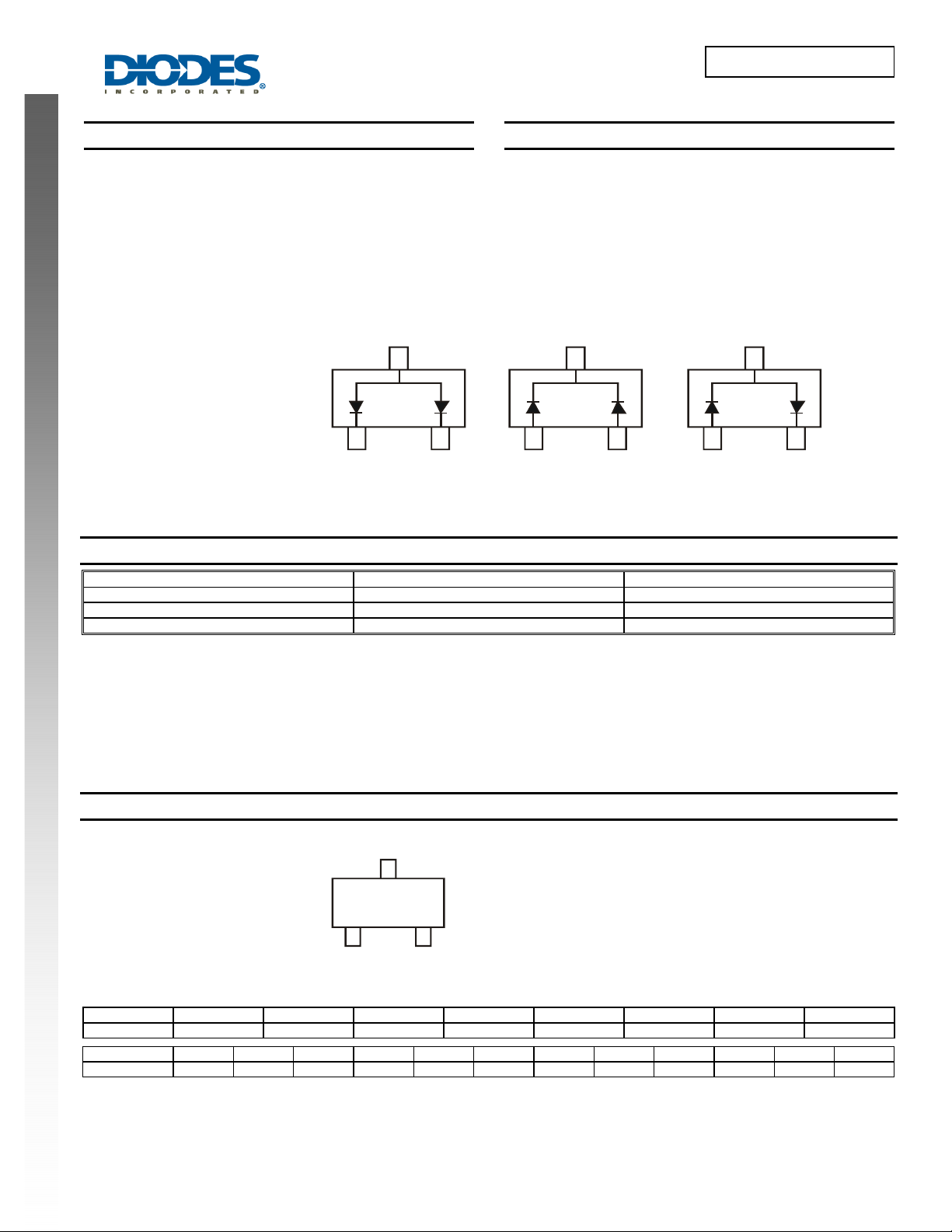
Mechanical Data
• Case: SOT23
• Case Material: Molded Plastic. "Green" Molding Compound.
UL Flammability Classification Rating 94V-0
• Moisture Sensitivity: Level 1 per J-STD-020
• Terminals: Finish - Matte Tin annealed over Alloy 42 leadframe.
Solderable per MIL-STD-202, Method 208
• Polarity: See Diagram
• Weight: 0.008 grams (approximate)
Ordering Information (Note 4)
Part Number Case Packaging
MMBD5004S-7 SOT23 3000/Tape & Reel
MMBD5004C-7 SOT23 3000/Tape & Reel
MMBD5004A-7 SOT23 3000/Tape & Reel
Notes: 1. No purposely added lead. Fully EU Directive 2002/95/EC (RoHS) & 2011/65/EU (RoHS 2) compliant.
2. See http://www.diodes.com/quality/lead_free.html for more information about Diodes Incorporated’s definitions of Halogen and Antimony free, "Green"
and Lead-Free.
3. Halogen and Antimony free "Green” products are defined as those which contain <900ppm bromine, <900ppm chlorine (<1500ppm total Br + Cl) and
<1000ppm antimony compounds.
4. For packaging details, go to our website at http://www.diodes.com.
Marking Information
Date Code Key
Year 2010 2011 2012 2013 2014 2015 2016 2017
Code X Y Z A B C D E
Month Jan Feb Mar Apr May Jun Jul Aug Sep Oct Nov Dec
Code 1 2 3 4 5 6 7 8 9 O N D
Top View
SOT23
MMBD5004S
xxx = Product Type Marking Code
ex. KJB = MMBD5004S
CJK = MMBD5004C
AJK = MMBD5004A
YM = Date Code Marking
Y = Year (ex: Y = 2011)
M = Month (ex: 9 = September)
MMBD5004A
MMBD5004C
xxx
YM
MMBD5004A/C/S
Document number: DS35585 Rev. 2 - 2
2 of 4
www.diodes.com
April 2012
© Diodes Incorporated
MMBD5004
A
/C/S
NEW PRODUCT
Maximum Ratings @T
A
= 25°C unless otherwise specified
Characteristic Symbol Value Unit
Repetitive Peak Reverse Voltage
V
RRM
400 V
Working Peak Reverse Voltage
DC Blocking Voltage
V
RWM
V
R
350 V
RMS Reverse Voltage
V
R
(
RMS
)
247 V
Forward Continuous Current (Note 5)
I
F
300 mA
Peak Repetitive Forward Current (Note 5)
I
FRM
625 mA
Non-Repetitive Peak Forward Surge Current @ t = 1.0
μ
s
@ t = 1.0ms
I
FSM
5
3
A
Thermal Characteristics
Characteristic Symbol Value Unit
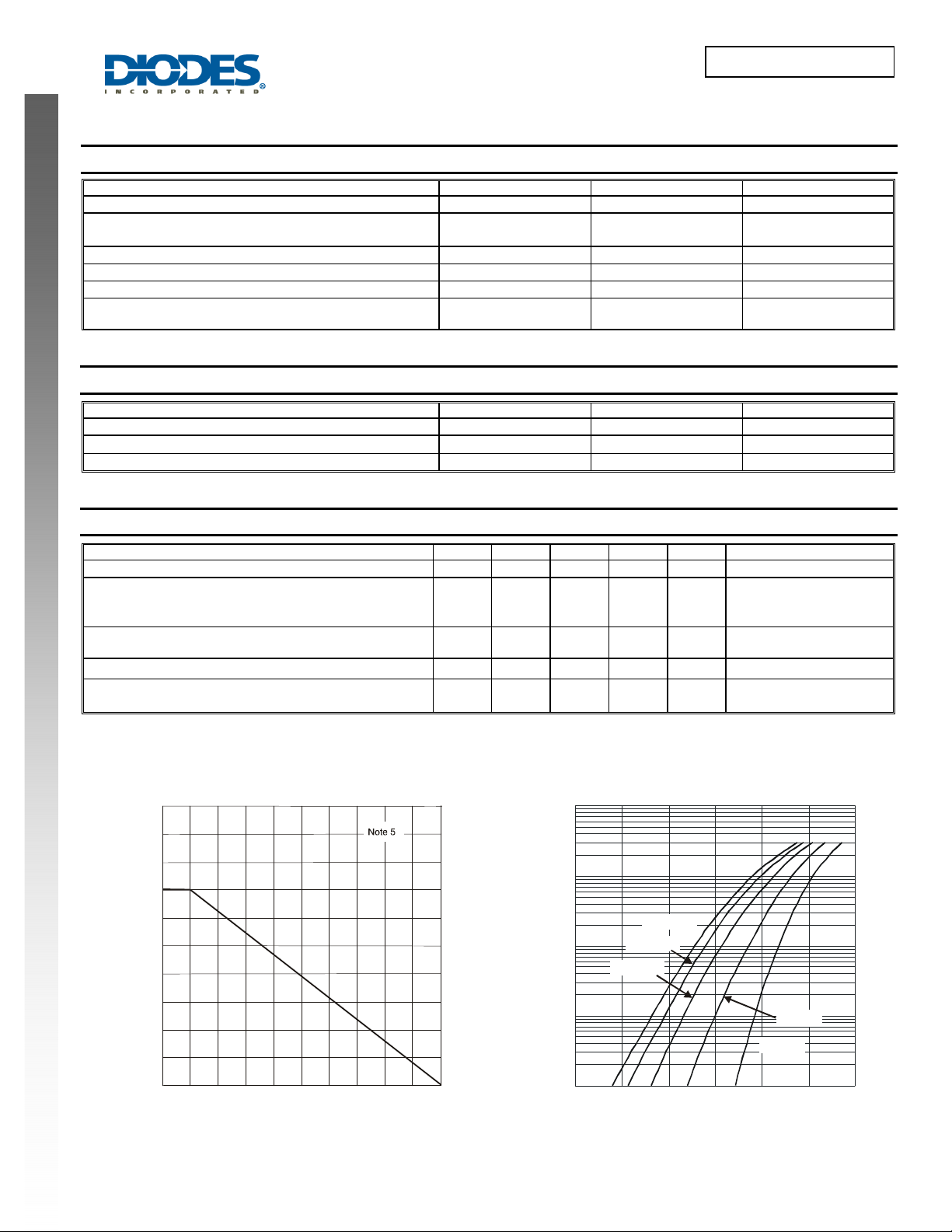
Power Dissipation (Note 5) (See figure 1)
P
D
350 mW
Thermal Resistance Junction to Ambient Air (Note 5)
R
θ
JA
357
°C/W
Operating and Storage Temperature Range
T
J
, T
STG
-55 to +150
°C
Electrical Characteristics @T
A
= 25°C unless otherwise specified
Characteristic Symbol Min Typ Max Unit Test Condition
Reverse Breakdown Voltage (Note 6)
V
(
BR
)
R
400
⎯ ⎯
V
I
R
= 150μA
Forward Voltage
V
F
⎯
⎯
⎯
⎯
0.9
1.05
1.275
V
I
F
= 20mA
I
F
= 100mA
I
F
= 200mA
Reverse Current (Note 6)
I
R
⎯
⎯
⎯
150
5
nA
μA
V
R
= 240V
V
R
= 360V
Total Capacitance
C
T
⎯
0.65 2.0 pF
V
R
= 0V, f = 1.0MHz
Reverse Recovery Time
t
rr
⎯ ⎯
50 ns
I
F
= I
R
= 30mA,
I
rr
= 3.0mA, R
L
= 100Ω
Notes: 5. Part mounted on FR-4 board with recommended pad layout, which can be found on our website at http://www.diodes.com.
6. Short duration pulse test used to minimize self-heating effect.
400
T , AMBIENT TEMPERATURE (°C)
Fig. 1 Power Derating Curve, Total Package
A
P
,
P
O
WE
R
DISSI
P
A
T
I
O
N (mW )
D
200
100
300
0
500
0
30 60 90 120 150
I , INSTANTANEOUS FORWARD CURRENT ( A)
F
m
100
1
10
0.1
1,000
V , INSTANT ANEOUS FO RWARD VOLTAGE (V)
Fig. 2 Typical Forwar d C haracteristics, P er Element
F
0 0.2 0.4 0.6 0.8 1.0
1.2
T = 150 C
J
°
T = 1 C
J
25
°
T = C
J
85
°
T = 25C
J
°
T = 5C
J
-5
°
 Loading...