


Description
The AP3105NA/NV/NL/NR is a low startup current, current mode PWM controller with green-mode power-saving operation. The PWM switching frequency at normal operation is set with 65kHz typically and the dithering of frequency will also improve the EMI feature. When the load decreases, the frequency will reduce and when at a very low load, the IC will enter the ‘burst mode’ to minimize switching loss.
About 20kHz frequency switching is to avoid the audible noise as well as reducing the standby loss. The skip mode point can be adjusted through the external resistor connected to the current sense resistor.
The AP3105NA/NV/NL/NR features a lot of functions such as the Leading-Edge Blanking (LEB) of the current sensing, internal slope compensation and several protection functions including cycle-by- cycle current limit (OCP), VCC Over Voltage Protection (VOVP), OTP and OLP protection. The versatile latch function can be set by the customer through few components.
This IC is available in SOT-23-6 package.
A Product Line of
Diodes Incorporated
AP3105NA/NV/NL/NR
COST EFFECTIVE GREEN PWM CONTROLLER
Pin Assignments
K Package (SOT-23-6)
Pin 1 Mark
GND |
1 |
6 |
GATE |
FB |
2 |
5 |
VCC |
CTRL |
3 |
4 |
SENSE |
Features |
|
Applications |
||
Very Low Start-up Current |
|
|
Switching AC-DC Adapter/Charger |
|
|
Current Mode Control |
|
|
ATX/BTX Auxiliary Power |
|
Non-audible-noise Green-mode Control |
|
Set-top Box(STB) Power Supply |
|
|
Skip Mode Adjustable |
|
Open Frame Switching Power Supply |
|
Internal Slope Compensation
Soft Start During Startup Process
Frequency Fold Back for High Average Efficiency
Secondary Short Winding Protection with FOCP
Soft Switching for Reducing EMI
VCC Maintain Mode
Latch Function for OTP/OVP
Useful Pin Fault Protection:
SENSE Pin Floating
CTRL Pin Short to Ground
FB/Opto-coupler Open/Short
Comprehensive System Protection Feature: VCC Over Voltage Protection (VOVP) Over Load Protection (OLP)
Mini Size with Packages
Pin to Pin Compatible with AP3103
AP3105NA/NV/NL/NR |
1 of 13 |
September 2013 |
Document number: DS36542 Rev. 1 - 2 |
www.diodes.com |
© Diodes Incorporated |

A Product Line of
Diodes Incorporated
AP3105NA/NV/NL/NR
Typical Applications Circuit
T1 |
L2 |
|
|
+ |
|
|
|
|
C6 |
|
|
|
|
|
R6 |
C5 |
|
|
|
|
C2 |
R4 |
|
|
||
|
|
|
R13 |
|
C8 |
||
|
|
|
|
C7 |
|||
|
|
|
|
|
|||
|
|
|
|
|
|
||
|
|
|
|
|
|
|
|
~ |
- |
|
R5 |
|
|
|
|
~ |
|
|
|
|
|
|
|
|
|
|
|
R19 |
|
|
|
|
|
|
|
C4 |
|
|
|
|
|
|
|
|
|
|
R14 |
|
|
U1 |
C3 |
|
|
|
|
|
|
|
|
|
|
|
|
|
NTC |
|
|
|
R8 |
|
|
R2 |
R3 |
|
|
|
|
|
|
|
|
VCC |
GATE |
|
|
|
|
C1 |
|
|
|
|
R10 |
|
|
|
|
|
|
R9 |
|
R15 |
|
|
|
CTRL |
SENSE |
|
C10 |
||
|
|
C11 |
|
R16 |
|||
|
|
AP3105NA/ |
R11 |
R12 |
|||
|
R7 |
|
R17 |
||||
|
|
|
|
|
|||
VR1 |
NV/NL/NR |
|
|
AZ431 |
C9 |
||
|
|
|
|||||
F1 |
|
|
FB |
|
|
|
|
|
NTC |
|
|
|
|
|
|
|
GND |
|
|
|
R18 |
||
|
|
|
|
|
|||
~ |
|
|
|
|
|
|
U2 |
|
|
|
|
|
|
|
|
Pin Descriptions
Pin Number |
Pin Name |
|
|
1 |
GND |
|
|
2 |
FB |
3CTRL
4SENSE
5 |
VCC |
|
|
6 |
GATE |
Function
Signal ground. Current return for driver and control circuits
Feedback. Directly connected to the opto-coupler
Latch trigger if this pin voltage drops below a threshold or over another threshold, leave CTRL pin open if this function is not needed. Connecting a NTC thermistor to GND can achieve OTP protection
Current Sense
Supply voltage of driver and control circuits
Gate driver output
AP3105NA/NV/NL/NR |
2 of 13 |
September 2013 |
Document number: DS36542 Rev. 1 - 2 |
www.diodes.com |
© Diodes Incorporated |
A Product Line of
Diodes Incorporated
AP3105NA/NV/NL/NR
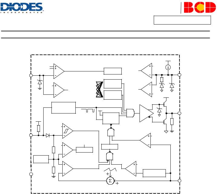
Functional Block Diagram
|
15.5V |
|
|
|
2.5V |
100 uA |
|
|
8.6V |
UVLO |
UVLO |
Internal |
CTRL_H |
|
|
|
3 |
|
|||||
VCC |
5 |
|
|
Bias |
|
CTRL |
|
|
|
|
|
|
|||
|
|
|
|
10K |
|
||
|
32V |
|
OLP |
Auto |
|
|
|
|
|
|
|
|
|||
|
|
Recovery |
|
|
|
||
|
28V |
|
VCC_OVP |
0.6V |
3.6V |
|
|
|
|
Protection |
|
||||
|
|
OVP |
VCC_OVP FOCP |
|
CTRL_L |
|
|
|
|
|
CTRL_H |
Latch -off |
0.5V |
|
|
|
|
|
CTRL_L |
Protection |
|
|
|
|
|
OSC with |
|
|
|
|
|
|
|
Frequency Jitter |
|
Driver 13V |
6 |
GATE |
|
|
|
|
D |
DFF Q |
|||
|
|
|
|
|
|
||
|
|
|
CLKRB |
|
|
|
|
|
|
0.5V |
Burst |
|
|
|
|
FB |
2 |
|
|
1.8V |
|
|
|
FOCP |
|
||
|
|
|
|
|
|
|
|
1.25V |
OLP |
|
|
|
|
250ns LEB |
|
|
|
|
|
|
|
|
|
|
2R |
|
64ms Delay |
|
|
|
Soft Start |
|
|
|
|
|
|
|
|
0.95V |
|
|
R |
PWM |
OCP |
Line |
|
|
|
|
|
||
GND |
1 |
|
|
|
|
|
|
Compensation |
|
||
|
|
|
|
4 |
SENSE |
|
|
|
|
|
AP3105NA/NV/NL/NR
AP3105NA/NV/NL/NR |
3 of 13 |
September 2013 |
Document number: DS36542 Rev. 1 - 2 |
www.diodes.com |
© Diodes Incorporated |

|
|
|
A Product Line of |
|
|
|
|
|
|
|
Diodes Incorporated |
|
|
|
|
|
|
|
|
|
|
|
|
|
|
|
|
AP3105NA/NV/NL/NR |
|
||
|
|
|
|
|
|
|
|
Absolute Maximum Ratings (Note 1) |
|
|
|
|
|
||
|
|
|
|
|
|
|
|
|
Symbol |
Parameter |
|
Rating |
Unit |
||
|
|
|
|
|
|
||
|
VCC |
Power Supply Voltage |
30 |
V |
|||
|
|
|
|
|
|
||
|
IO |
Gate Output Current |
350 |
mA |
|||
|
|
|
|
|
|
|
|
|
VFB, VSENSE, VCTRL |
Input Voltage to FB, SENSE, CTRL |
|
-0.3 to 7 |
V |
||
|
|
|
|
|
|
||
|
θJA |
Thermal Resistance (Junction to Ambient) |
250 |
°C/W |
|||
|
|
|
|
|
|
||
|
PD |
Power Dissipation at TA < +25°C |
500 |
mW |
|||
|
|
|
|
|
|
|
|
|
TJ |
Operating Junction Temperature |
|
-40 to +150 |
°C |
||
|
|
|
|
|
|
||
|
TSTG |
Storage Temperature Range |
+150 |
°C |
|||
|
|
|
|
|
|
|
|
|
– |
ESD (Human Body Model) |
3000 |
V |
|||
|
|
||||||
|
|
|
|
|
|
|
|
|
– |
ESD (Machine Model) |
300 |
V |
|||
|
|
||||||
|
|
|
|
|
|
|
|
Note 1: Stresses greater than those listed under “Absolute Maximum Ratings” may cause permanent damage to the device. These are stress ratings only, and functional operation of the device at these or any other conditions beyond those indicated under “Recommended Operating Conditions” is not implied. Exposure to “Absolute Maximum Ratings” for extended periods may affect device reliability.
Recommended Operating Conditions
Symbol |
|
Parameter |
Min |
Max |
Unit |
|
|
|
|
|
|
VCC |
Supply Voltage |
|
10 |
25 |
V |
|
|
|
|
|
|
AP3105NA/NV/NL/NR |
4 of 13 |
September 2013 |
Document number: DS36542 Rev. 1 - 2 |
www.diodes.com |
© Diodes Incorporated |
 Loading...