


NEW PRODUCT
Description
The PAM8304 is a mono filter-less Class-D amplifier with high SNR and differential input that helps eliminate noise. The PAM8304 supports 2.8V to 6V operation make it idea for up to 4 cells alkaline battery applications. The PAM8304 is capable of driving speaker loads as low as 3Ω speaker with a 5V supply maximizing the output power.
Features like greater than 90% efficiency and small PCB area make the PAM8304 Class-D amplifier ideal for portable applications. The output uses a filter-less architecture minimizing the number of external components and PCB area whilst providing a high performance, simple and lower cost system.
The PAM8304 features short circuit protection, thermal shutdown and under voltage lock-out.
The PAM8304 is available in DFN3030-8L and MOP-8L packages.
Features
Supply Voltage from 2.8V to 6.0 V
3Ω Driving Capability
3.0W@10% THD Output with a 4Ω Load and 5V Supply
High Efficiency up to 90% @1W with an 8Ω Load
Shutdown Current <1μA
Superior Low Noise without Input
Short Circuit Protection
Thermal Shutdown
Available in Space Saving DFN3030-8L and MSOP-8L Packages
Pb-Free Package
A Product Line of
Diodes Incorporated
PAM8304
3W MONO CLASS D AUDIO AMPLIFIER
Pin Assignments
|
|
DFN3X3-8L |
|
|
|
|
Top View |
|
|
OUT+ |
1 |
|
8 |
OUT- |
PVDD |
2 |
P8304 XXXYW |
7 |
GND |
VDD 3 |
6 |
SD |
||
IN- |
4 |
|
5 |
IN+ |
MSOP-8L
Top View
OUT+ 1 8 OUT-
VDD |
3 |
304P8 XXXYW |
6 |
SD |
|
PVDD |
2 |
|
7 |
GND |
|
|
|
|
|
|
|
IN- |
4 |
|
5 |
IN+ |
|
Applications
MP4/MP3
GPS
Set-Top-Box
Tablets/Digital Photo Frame
Electronic Dictionary
Portable Game Machines
Typical Applications Circuit
|
|
|
|
|
|
|
|
|
|
|
|
|
V D D |
|
|
|
|
|
|
|
|
|
|
|||||
|
|
|
|
|
|
|
|
|
|
|
|
|
|
|
|
|
|
|
|
|
|
1μ F |
|
|
|
|||
|
|
|
|
|
|
|
|
|
|
|
|
|
|
|
|
|
|
|
|
|
|
|
|
|
||||
|
|
|
|
|
|
|
|
|
|
|
|
|
|
|
|
|
|
|
|
|
|
|
|
|
||||
|
|
|
|
|
|
|
|
|
|
|
|
|
|
|
|
|
|
|
|
|
|
|
|
|||||
|
|
|
|
|
|
|
|
|
|
|
|
|
|
|
|
|
|
|
|
|
|
|
|
|
|
|
|
|
|
|
|
|
|
|
|
|
|
|
|
|
|
|
|
|
|
|
|
|
|
|
|
|
|
|
|
|
|
|
|
|
|
|
|
|
|
|
|
|
|
|
|
|
|
|
|
|
|
|
|
|
|
|
|
|
|
|
|
|
|
|
|
|
|
|
|
|
|
|
P V D D |
|
|
|
V D D |
|
|
|
|||||||||
V I N |
|
|
0.1μ F |
I N + |
|
|
|
|
|
|
|
|
|
|
|
|
|
|
|
|
|
|||||||
|
|
|
|
|
|
|
|
|
|
|
|
|
|
|
|
|
|
|
|
OU T+ |
|
|
|
|||||
|
|
|
|
|
|
|
|
|
|
|
|
|
|
|
|
|
|
|
|
|
|
|
||||||
|
|
|
|
|
|
0.1μ F |
|
|
|
|
|
|
|
|
|
|
|
|
|
|
|
|
|
|||||
|
|
|
|
|
|
I N - |
|
PA M 8 3 0 4 |
|
|
|
|||||||||||||||||
|
|
|
|
|
|
|
|
|
|
|
|
|
|
|
||||||||||||||
|
|
|
|
|
|
|
|
|
|
|
|
|
|
|
|
|
|
|
|
|
|
|
|
|
|
|
|
|
|
/ S D |
|
|
|
|
|
/ S D |
|
|
|
|
|
|
|
|
|
|
|
|
|
OU T- |
|
|
|
||||
|
|
|
|
|
|
|
|
|
|
|
|
|
|
|
|
|
|
|
|
|
|
|||||||
|
|
|
|
|
|
|
|
|
|
|
|
|
|
|
|
|
|
|
|
|
||||||||
|
|
|
|
|
|
|
|
|
|
|
|
|
|
|
|
|
|
|
|
|
|
|
|
|
|
|
|
|
|
|
|
|
|
|
|
|
|
|
|
|
P GN D |
|
|
|
GN D |
|
|
|
|||||||||
|
|
|
|
|
|
|
|
|
|
|
|
|
|
|
|
|
|
|
|
|
|
|
|
|
|
|
|
|
PAM8304 |
1 of 11 |
October 2013 |
Document number: DS36589 Rev. 1 - 2 |
www.diodes.com |
© Diodes Incorporated |
NEW PRODUCT
A Product Line of
Diodes Incorporated
PAM8304
Pin Descriptions
Pin Name |
MSOP-8L/DFN3x3-8L |
Function |
OUT+ |
1 |
Positive BTL Output |
PVDD |
2 |
Power Supply |
VDD |
3 |
Analog Power Supply |
IN- |
4 |
Negative Differential Input |
IN+ |
5 |
Positive Differential Input |
/SD |
6 |
Shutdown Terminal, Active Low |
GND |
7 |
Ground |
OUT- |
8 |
Negative BTL Output |
Exposed Pad |
— |
NC |
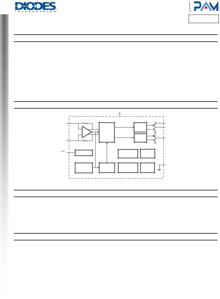
Functional Block Diagram
|
|
|
VDD |
|
|
|
IN+ |
|
|
|
Gate |
|
PVDD |
|
|
|
|
|
OUT+ |
|
|
- |
PWM |
|
Drive |
|
|
|
+ |
Modulator |
|
|
|
|
IN- |
|
|
Gate |
|
OUT- |
|
|
|
|
Drive |
|
||
|
|
|
|
|
|
|
SD |
SD |
|
UVLO |
|
SC |
|
|
|
|
|
Protect |
|
|
|
Bias and |
OSC |
Startup |
OTP |
GND |
|
|
Vref |
Protection |
|
|||
|
|
|
|
|
||
Absolute Maximum Ratings (@TA = +25°C, unless otherwise specified.)
Parameter |
Rating |
Unit |
Supply Voltage (VDD) |
6.5 |
V |
Input Voltage (IN+, IN-, /SD) |
-0.3 to VDD +0.3 |
V |
Storage Temperature |
-65 to +150 |
°C |
Maximum Junction Temperature |
150 |
°C |
Recommended Operating Conditions (@TA = +25°C, unless otherwise specified.)
Symbol |
Parameter |
Min |
Max |
Unit |
VDD |
Supply Voltage |
2.8 |
6.0 |
V |
TA |
Operating Ambient Temperature Range |
-40 |
+85 |
°C |
TJ |
Junction Temperature Range |
-40 |
+125 |
°C |
PAM8304 |
2 of 11 |
October 2013 |
Document number: DS36589 Rev. 1 - 2 |
www.diodes.com |
© Diodes Incorporated |

A Product Line of
Diodes Incorporated
PAM8304
Electrical Characteristics (@TA=25°C, VDD=5V, Gain=18dB, RL=L(33μH)+R+L(33μH), unless otherwise noted.)
NEW PRODUCT
Symbol |
Parameter |
Test Conditions |
|
Min |
Typ |
|
Max |
Unit |
VDD |
Supply Voltage |
|
|
2.8 |
|
6.0 |
V |
|
|
|
THD+N = 10%, f = 1kHz, |
VDD = 5.0V |
|
3.0 |
|
|
|
|
|
VDD = 3.6V |
|
1.5 |
|
|
W |
|
|
|
R = 4Ω |
|
|
|
|||
|
|
VDD = 3.2V |
|
1.2 |
|
|
|
|
|
|
|
|
|
|
|
||
|
|
THD+N = 1%, f = 1kHz, |
VDD = 5.0V |
|
2.4 |
|
|
|
|
|
VDD = 3.6V |
|
1.25 |
|
|
W |
|
|
|
R = 4Ω |
|
|
|
|||
Po |
Output Power |
VDD = 3.2V |
|
1.0 |
|
|
|
|
|
|
|
|
|
||||
THD+N = 10%, f = 1kHz, |
VDD = 5.0V |
|
1.75 |
|
|
|
||
|
|
|
|
|
|
|||
|
|
VDD = 3.6V |
|
0.90 |
|
|
W |
|
|
|
R = 8Ω |
|
|
|
|||
|
|
VDD = 3.2V |
|
0.70 |
|
|
|
|
|
|
|
|
|
|
|
||
|
|
THD+N = 1%, f = 1kHz, |
VDD = 5.0V |
|
1.40 |
|
|
|
|
|
VDD = 3.6V |
|
0.72 |
|
|
W |
|
|
|
R = 8Ω |
|
|
|
|||
|
|
VDD = 3.2V |
|
0.60 |
|
|
|
|
|
|
|
|
|
|
|
||
|
|
VDD = 5.0V, Po = 1W, R = 8Ω |
|
|
0.17 |
|
|
|
|
Total Harmonic |
VDD = 3.6V, Po = 0.1W, R = 8Ω |
f = 1kHz |
|
0.16 |
|
|
% |
|
VDD = 3.2V, Po =0.1W, R = 8Ω |
|
|
0.14 |
|
|
|
|
THD+N |
Distortion Plus |
|
|
|
|
|
||
VDD = 5.0V, Po = 0.5W, R = 4Ω |
|
|
0.14 |
|
|
|
||
|
Noise |
|
|
|
|
|
||
|
|
VDD = 3.6V, Po = 0.2W, R = 4Ω |
f = 1kHz |
|
0.16 |
|
|
% |
|
|
VDD = 3.2V, Po = 0.1W, R = 4Ω |
|
|
0.17 |
|
|
|
|
Power Supply Ripple |
VDD = 3.6V, Inputs ac-grounded |
f=217Hz |
|
-68 |
|
|
|
PSRR |
f=1kHz |
|
-70 |
|
|
dB |
||
Rejection |
with C = 1μF |
|
|
|
||||
|
f=10kHz |
|
-67 |
|
|
|
||
|
|
|
|
|
|
|
||
Dyn |
Dynamic Range |
VDD = 5V,THD = %, R = 8Ω |
f=1kHz |
|
95 |
|
|
dB |
|
|
|
No A |
|
170 |
|
|
|
Vn |
Output Noise |
Inputs ac-grounded |
weighting |
|
|
|
μV |
|
|
|
|
|
|||||
|
|
|
A-weighting |
|
130 |
|
|
|
η |
Efficiency |
RL = 8Ω,THD = 10% |
f=1kHz |
|
93 |
|
|
% |
RL = 4Ω,THD = 10% |
|
86 |
|
|
||||
|
|
|
|
|
|
|
||
IQ |
Quiescent Current |
VDD = 5V |
No Load |
|
5 |
|
|
mA |
Isd |
Shutdown Current |
VDD = 2.8V to 5V |
/SD=0V |
|
|
1 |
μA |
|
Rdson |
Static Drain-to Source On- |
High Side PMOS,I = 500mA |
VDD=5.0V |
|
325 |
|
|
mΩ |
state Resistor |
Low Side NMOS,I = 500mA |
VDD=5.0V |
|
200 |
|
|
mΩ |
|
|
|
|
|
|||||
fsw |
Switching Frequency |
VDD = 2.8V to 5V |
|
|
400 |
|
|
kHz |
Gv |
Closed-loop Gain |
VDD = 2.8V to 5V |
|
|
300K/Rin |
|
|
V/V |
Vos |
Output Offset Voltage |
Input ac-ground, VDD = 5V |
|
|
|
50 |
mV |
|
VIH |
SD Input High Voltage |
VDD = 5V |
|
1.4 |
|
|
|
V |
VIL |
SD Input Low Voltage |
VDD = 5V |
|
|
|
1.0 |
||
|
|
|
|
|||||
PAM8304 |
3 of 11 |
October 2013 |
Document number: DS36589 Rev. 1 - 2 |
www.diodes.com |
© Diodes Incorporated |

A Product Line of
Diodes Incorporated
|
|
|
|
|
|
|
|
|
|
|
|
|
|
PAM8304 |
|||
|
Performance Characteristics (@TA=25°C, VDD=5V, Gain=18dB, RL=L(33μH)+R+L(33μH), unless otherwise noted.) |
|
|
|
|||||||||||||
|
|
THD+N Vs. Output Power (RL=4Ω) |
|
|
|
|
THD+N Vs. Output Power (RL=8Ω) |
|
|
||||||||
|
2 0 |
|
|
|
|
|
|
|
2 0 |
|
|
|
|
|
|
|
|
PRODUCT |
1 0 |
|
|
|
|
|
|
|
1 0 |
|
|
|
|
|
|
|
|
5 |
|
|
VDD=5.0V |
|
|
|
5 |
|
|
|
VDD=5.0V |
|
|
|
|||
|
|
|
|
|
|
|
|
|
|
|
|
|
|
||||
2 |
|
|
|
|
|
|
|
2 |
|
|
|
VDD=3.6V |
|
|
|
||
% |
|
|
VDD=3.6V |
|
|
|
|
% |
|
|
|
|
|
|
|||
1 |
|
|
|
|
|
|
1 |
|
|
|
|
|
|
|
|||
0 .5 |
|
|
|
|
|
|
|
0 .5 |
|
|
|
|
|
|
|
||
|
|
|
|
|
|
|
|
|
|
|
|
|
|
|
|||
|
|
|
|
|
|
|
|
|
|
|
|
|
|
|
|
||
NEW |
0 .2 |
|
|
|
|
|
|
|
0 .2 |
|
|
|
|
|
|
|
|
|
|
|
|
|
|
|
|
|
|
|
|
|
|
|
|||
0 .1 |
|
|
|
|
|
|
|
0 .1 |
|
|
|
|
|
|
|
||
1 m |
2 m |
5 m 1 0m 2 0 m |
5 0 m 10 0 m 2 00 m |
5 0 0m |
1 |
2 |
5 |
|
|
|
|
|
|
|
|||
1 m |
2 m |
5 m |
1 0 m 2 0 m |
50 m 1 0 0 m 2 0 0 m |
500m |
1 |
2 3 |
||||||||||
|
|
|
W |
|
|
|
|
||||||||||
|
|
|
|
|
|
|
|
|
|
|
|
W |
|
|
|
||
|
|
|
|
|
|
|
|
|
|
|
|
|
|
|
|
||
THD+N Vs. Frequency
|
1 0 |
|
|
|
|
|
|
|
|
|
|
Po=300mW |
|
|
|
|
|
|
|
|
|
|
5 |
|
|
|
|
|
|
|
|
|
|
2 |
|
|
|
VDD=5.0V |
|
|
|
|
|
|
1 |
|
|
|
|
|
|
|
|
|
% |
0 . 5 |
|
|
VDD=3.6V |
|
|
|
|
|
|
|
|
|
|
|
|
|
|
|||
|
|
|
|
|
|
|
|
|
||
|
0 . 2 |
|
|
|
|
|
|
|
|
|
|
0 . 1 |
|
|
|
|
|
|
|
|
|
|
0 . 0 5 |
|
|
|
|
|
|
|
|
|
|
0 . 0 22 0 |
5 0 |
1 0 0 |
2 0 0 |
5 0 0 |
1 k |
2 k |
5 k |
1 0 k |
2 0 k |
|
|
|
|
|
H z |
|
|
|
|
|
PSRR Vs. Frequency
|
+0 |
T |
|
|
|
|
|
|
|
|
|
-5 |
|
|
|
|
|
|
|
|
|
|
|
|
|
|
|
|
|
|
|
|
|
-10 |
VDD=5.0V |
|
|
|
|
|
|
|
|
|
-15 |
|
|
|
|
|
|
|
||
|
|
|
|
|
|
|
|
|
|
|
|
-20 |
|
|
|
|
|
|
|
|
|
|
-25 |
|
|
|
|
|
|
|
|
|
|
-30 |
|
|
|
|
|
|
|
|
|
|
-35 |
|
|
|
|
|
|
|
|
|
d |
-40 |
|
|
|
|
|
|
|
|
|
B |
|
|
|
|
|
|
|
|
|
|
|
|
|
|
|
|
|
|
|
|
|
|
-45 |
|
|
|
|
|
|
|
|
|
|
-50 |
|
|
|
|
|
|
|
|
|
|
-55 |
|
|
|
|
|
|
|
|
|
|
-60 |
|
|
|
|
|
|
|
|
|
|
-65 |
|
|
|
|
|
|
|
|
|
|
-70 |
|
|
|
|
|
|
|
|
|
|
-75 |
|
|
|
|
|
|
|
|
|
|
-80 |
50 |
100 |
200 |
500 |
1k |
2k |
5k |
10k |
20k |
|
20 |
|||||||||
|
|
|
|
|
Hz |
|
|
|
|
|
Frequency Response
|
+ 2 0 |
|
|
|
|
|
|
|
|
|
|
|
+ 1 9 . |
5 |
|
|
|
|
|
|
|
|
|
|
+ 1 9 |
|
|
|
|
|
|
|
|
|
|
|
+ 1 8 . |
5 |
|
|
|
|
|
|
|
|
|
|
+ 1 8 |
|
|
|
|
|
|
|
|
|
|
|
+ 1 7 . |
5 |
|
|
|
|
|
|
|
|
|
|
+ 1 7 |
|
|
|
|
|
|
|
|
|
|
|
+ 1 6 . |
5 |
|
|
|
|
|
|
|
|
|
|
+ 1 6 |
|
|
|
|
|
|
|
|
|
|
d |
+ 1 5 . |
5 |
|
|
|
|
|
|
|
|
|
B |
|
|
|
|
|
|
|
|
|
||
+ 1 5 |
|
|
|
|
|
|
|
|
|
||
g |
|
|
|
|
|
|
|
|
|
||
A |
+ 1 4 . |
5 |
|
|
|
|
|
|
|
|
|
|
|
|
|
|
|
|
|
|
|
|
|
|
+ 1 4 |
|
|
|
|
|
|
|
|
|
|
|
+ 1 3 . |
5 |
|
|
|
|
|
|
|
|
|
|
+ 1 3 |
|
|
|
|
|
|
|
|
|
|
|
+ 1 2 . |
5 |
|
|
|
|
|
|
|
|
|
|
+ 1 2 |
|
|
|
|
|
|
|
|
|
|
|
+ 1 1 . |
5 |
|
|
|
|
|
|
VDD=5.0V |
|
|
|
+ 1 1 |
|
|
|
|
|
|
|
|||
|
+ 1 0 . |
5 |
|
|
|
|
|
|
|
|
|
|
+ 1 02 0 |
5 0 |
1 0 0 |
2 00 |
5 0 0 |
1 k |
2k |
5 k |
10 k |
2 0k |
|
|
|
|
|
|
|
|
H z |
|
|
|
|
Noise Floor
|
+ 20 |
|
|
|
|
|
|
|
|
|
|
+ 10 |
VDD=5.0V |
|
|
|
|
|
|
|
|
|
+ 0 |
|
|
|
|
|
|
|
||
|
|
|
|
|
|
|
|
|
||
|
-10 |
|
|
|
|
|
|
|
|
|
|
-20 |
|
|
|
|
|
|
|
|
|
|
-30 |
|
|
|
|
|
|
|
|
|
d |
-40 |
|
|
|
|
|
|
|
|
|
B |
-50 |
|
|
|
|
|
|
|
|
|
r |
|
|
|
|
|
|
|
|
|
|
A |
-60 |
|
|
|
|
|
|
|
|
|
|
-70 |
|
|
|
|
|
|
|
|
|
|
-80 |
|
|
|
|
|
|
|
|
|
|
-90 |
|
|
|
|
|
|
|
|
|
|
-100 |
|
|
|
|
|
|
|
|
|
|
-110 |
|
|
|
|
|
|
|
|
|
|
-12020 |
50 |
100 |
200 |
500 |
1k |
2k |
5k |
10k |
20k |
|
|
|
|
|
|
Hz |
|
|
|
|
PAM8304 |
4 of 11 |
October 2013 |
Document number: DS36589 Rev. 1 - 2 |
www.diodes.com |
© Diodes Incorporated |
 Loading...