


Diodes AP2552AFDC, AP2552AW6, AP2552FDC, AP2552W6, AP2553AFDC Schematic [ru]
...AP2552/ AP2553/ AP2552A/ AP2553A
PRECISION ADJUSTABLE CURRENT-LIMITED POWER SWITCHES
Description
The AP2552/53 and AP2552A/53A are single channel precision adjustable current-limited switches optimized for applications that require precision current limiting, or to provide up to 2.1A of continuous load current during heavy loads/short circuits. These devices offer a programmable current-limit threshold between 75mA and 2.36A (typ) via an external resistor. Current limit accuracy ±6% can be achieved at high current-limit settings. The rise and fall times are controlled to minimize current surges during turn on/off.
The devices have fast short-circuit response time for improved overall system robustness. They provide a complete protection solution for applications subject to heavy capacitive loads and the prospect of short circuit, offering reverse current blocking and limiting, overcurrent, over-temperature and short-circuit protection, as well as controlled rise time and under-voltage lockout functionality. A 7ms deglitch capability on the open-drain Flag output prevents false over-current reporting and does not require any external components.
Pin Assignments
|
(Top View) |
|
|
OUT |
1 |
6 |
IN |
ILIM |
2 |
PAD 5 |
GND |
|
3 |
4 |
EN |
FAULT |
|||
U-DFN2020-6
|
Top View |
|
|
IN |
1 |
6 |
OUT |
AP2552/53 limits the output current to a safe level when the output current exceeds current-limit threshold.
AP2552A/53A provides latch-off function during over-current or reverse-voltage conditions.
All devices are available in SOT26 and U-DFN2020-6 packages.
Applications
Set-Top Boxes
LCD TVs & Monitors
Residential Gateways
Laptops, Desktops, Servers, e-Readers, Printers, Docking Stations, HUBs
GND |
|
2 |
5 |
|
ILIM |
|
|
||||
EN |
|
3 |
4 |
|
FAULT |
|
|
||||
|
|
|
SOT26 |
|
|
Features
Up to 2.1A Maximum Load Current
Accurate Adjustable Current Limit, 75mA - 2360mA
±6% Accurate Adjustable Current Limit, 1.63A with RLIM = 15kΩ
Constant-Current (AP2552/53) During Over-Current
Output Latch-Off (AP2552A/53A) at Over-Current
Fast Short-Circuit Response Time: 2µs (typ)
Reverse Current Blocking During Shutdown and Reverse Current Limiting During Enable
Operating Range: 2.7V - 5.5V
Built-in Soft-Start with 3ms Typical Rise Time
Over-Current , Output Over-Voltage and Thermal Protection
Fault Report (FAULT) with Blanking Time
ESD Protection: 2kV HBM, 500V CDM
Active Low (AP2552/52A) or Active High (AP2553/53A) Enable
Ambient Temperature Range: -40ºC to +85°C
SOT26 and U-DFN2020-6 Package: Available in “Green” Molding Compound (No Br, Sb)
Totally Lead-Free & Fully RoHS Compliant (Notes 1 & 2)
Halogen and Antimony Free. “Green” Device (Note 3)
15kV ESD Protection per IEC 61000-4-2 (with external capacitance)
UL Recognized, File Number E322375, Vol. 1
1IEC60950-1 CB Scheme Certified
Notes: |
1. |
No purposely added lead. Fully EU Directive 2002/95/EC (RoHS) & 2011/65/EU (RoHS 2) compliant. |
|
2. |
See http://www.diodes.com/quality/lead_free.html for more information about Diodes Incorporated’s definitions of Halogenand Antimony-free, "Green" |
|
|
and Lead-free. |
|
3. |
Halogenand Antimony-free "Green” products are defined as those which contain <900ppm bromine, <900ppm chlorine (<1500ppm total Br + Cl) and |
|
|
<1000ppm antimony compounds. |
AP2552/AP2553/AP2552A/AP2553A |
1 of 17 |
October 2014 |
Document number: DS35404 Rev. 10 - 2 |
www.diodes.com |
© Diodes Incorporated |
AP2552/ AP2553/ AP2552A/ AP2553A
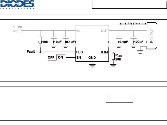
Typical Applications Circuit
120µF Output Capacitance is a Requirement of USB
Available Options
Part Number |
Channel |
Enable Pin (EN) |
Recommended Maximum |
Current-Limit |
Package |
|
Continuous Load Current (A) |
Protection |
|||||
|
|
|
|
|||
AP2552 |
1 |
Active Low |
2.1 |
Constant-Current |
U-DFN2020-6 |
|
AP2553 |
1 |
Active High |
SOT26 |
|||
|
|
|||||
AP2552A |
1 |
Active Low |
2.1 |
Latch-Off |
U-DFN2020-6 |
|
AP2553A |
1 |
Active High |
SOT26 |
|||
|
|
Pin Descriptions
|
|
Pin |
|
Pin Number |
|
I/O |
Function |
||||
|
Name |
AP2552W6-7 |
AP2553W6-7 |
AP2552FDC-7 |
AP2553FDC-7 |
||||||
|
|
|
|||||||||
|
|
IN |
1 |
1 |
6 |
6 |
I |
Input, connect a 0.1µF or greater ceramic capacitor from |
|||
|
|
IN to GND as close to IC as possible. |
|||||||||
|
|
|
|
|
|
|
|
|
|
||
|
GND |
2 |
2 |
5 |
5 |
— |
Ground, connect to external exposed pad. |
||||
|
|
|
|
|
3 |
— |
4 |
— |
I |
Enable input, logic low turns on power switch. |
|
|
|
EN |
|
|
|||||||
|
|
EN |
— |
3 |
— |
4 |
I |
Enable input, logic high turns on power switch. |
|||
|
|
|
|
|
4 |
4 |
3 |
3 |
O |
Active-low open-drain output, asserted during over- |
|
FAULT |
|||||||||||
current, over-temperature, or reverse-voltage conditions. |
|||||||||||
|
|
|
|
|
|
|
|
|
|
||
|
ILIM |
5 |
5 |
2 |
2 |
O |
Use external resistor to set current-limit threshold; |
||||
|
recommended 10kΩ RLIM 232kΩ. |
||||||||||
|
|
|
|
|
|
|
|
|
|
||
|
OUT |
6 |
6 |
1 |
1 |
O |
Output |
||||
Exposed |
|
|
|
|
|
No internal connection; recommend to connect to GND |
|||||
— |
— |
Pad |
Pad |
— |
externally for improved power dissipation. It should not be |
||||||
|
Pad |
||||||||||
|
|
|
|
|
|
used as electrical ground conduction path. |
|||||
|
|
|
|
|
|
|
|
|
|
||
AP2552/AP2553/AP2552A/AP2553A |
2 of 17 |
October 2014 |
Document number: DS35404 Rev. 10 - 2 |
www.diodes.com |
© Diodes Incorporated |
AP2552/ AP2553/ AP2552A/ AP2553A
Functional Block Diagram
|
|
|
|
|
|
|
|
|
|
|
|
|
|
|
|
|
|
|
|
|
|
|
|
|
|
|
|
|
|
|
|
|
|
|
|
|
|
|
|
|
|
|
|
|
|
|
|
|
|
|
|
|
|
|
|
|
|
|
|
|
|
|
|
|
|
|
|
|
|
|
|
|
|
|
|
|
|
|
|
|
|
|
|
|
|
|
|
|
|
|
|
|
|
|
|
|
|
|
|
|
|
|
|
|
|
|
|
|
|
|
|
|
|
|
|
|
|
|
|
|
|
|
|
|
|
|
|
|
|
|
|
|
|
|
|
|
|
|
|
|
|
|
|
|
|
|
|
|
|
|
|
|
|
|
|
|
|
|
|
|
|
|
|
|
|
|
|
|
|
|
|
|
|
|
|
|
|
|
|
|
|
|
|
|
|
|
|
|
|
|
|
|
|
|
|
|
|
|
|
|
|
|
|
|
|
|
|
|
|
|
|
|
|
|
|
|
|
|
|
|
|
|
|
|
|
|
|
|
|
|
|
|
|
|
|
|
|
|
|
|
|
|
|
|
|
|
|
|
|
|
|
|
|
|
|
|
|
|
|
|
|
|
|
|
|
|
|
|
|
|
|
|
|
|
|
|
|
|
|
|
|
|
|
|
|
|
|
|
|
|
|
|
|
|
|
|
|
|
|
|
|
|
|
|
|
|
|
|
|
|
|
|
|
|
|
|
|
|
|
|
|
|
|
|
|
|
|
|
|
|
|
|
|
|
|
|
|
|
|
|
|
|
|
|
|
|
|
|
|
|
|
|
|
|
|
|
|
|
|
|
|
|
|
|
|
|
|
|
|
|
|
|
|
|
|
|
|
|
|
|
|
|
|
|
|
|
|
|
|
|
|
|
|
|
|
|
|
|
|
|
|
|
|
|
|
|
|
|
|
|
|
|
|
|
|
|
|
|
|
|
|
|
|
|
|
|
|
|
|
|
|
|
|
|
|
|
|
|
|
|
|
|
|
|
|
|
|
|
|
|
|
|
|
|
|
|
|
|
|
|
|
|
|
|
|
|
|
|
|
|
|
|
|
|
|
|
|
|
|
|
|
|
|
|
|
|
|
|
|
|
|
|
|
|
|
|
|
|
|
|
|
|
|
|
|
|
|
|
|
|
|
|
|
|
|
|
|
|
|
|
|
|
|
|
|
|
|
|
|
|
|
|
|
|
|
|
|
|
|
|
|
|
|
|
|
|
|
|
|
|
|
|
|
|
|
|
|
|
|
|
|
|
|
|
|
|
|
|
|
|
|
|
|
|
|
|
|
|
|
|
|
|
|
|
|
|
|
|
|
|
|
|
|
|
|
|
|
|
|
|
|
|
|
|
|
|
|
|
|
|
|
|
|
|
|
|
|
|
|
|
|
|
|
|
|
|
|
|
|
|
|
|
|
|
|
|
|
|
|
|
|
|
|
|
|
|
|
|
|
|
|
|
|
|
|
|
|
|
|
|
|
|
|
|
|
|
|
|
|
|
|
|
|
|
|
|
|
|
|
|
|
|
|
|
|
|
|
|
|
|
|
|
|
|
|
|
|
|
|
|
|
|
|
|
|
|
|
|
|
|
|
|
|
|
|
|
|
|
|
|
|
|
|
|
|
|
|
|
|
|
|
|
|
|
|
|
|
|
|
|
|
|
|
|
|
|
|
|
|
|
|
|
|
|
|
|
|
|
|
|
|
|
|
|
|
|
|
|
|
|
|
|
|
|
|
|
|
|
|
|
|
|
|
|
|
|
|
|
|
|
|
|
|
|
|
|
|
|
|
|
|
|
|
|
|
|
|
|
|
|
|
|
|
|
|
|
|
|
|
|
|
|
|
|
|
|
|
|
|
|
|
|
|
|
|
|
|
|
|
|
|
|
|
|
|
|
|
|
|
|
|
|
|
|
|
|
|
|
|
|
|
|
|
|
|
|
|
|
|
|
|
|
|
|
|
|
|
|
|
|
|
|
|
|
|
|
|
|
|
|
|
|
|
|
|
|
|
|
|
|
|
|
|
|
|
|
|
|
|
|
|
|
|
|
|
|
|
|
|
|
|
|
|
|
|
|
|
|
|
|
|
|
|
|
|
|
|
|
|
|
|
|
|
|
|
|
|
|
|
|
|
|
|
|
|
|
|
|
|
|
|
|
|
|
|
|
|
|
|
|
|
|
|
|
|
|
|
|
|
|
|
|
|
|
|
|
|
|
|
|
|
|
|
|
|
|
|
|
|
|
|
|
|
|
|
|
|
|
|
|
|
|
|
|
|
|
|
|
|
|
|
|
|
|
|
|
|
|
|
|
|
|
|
|
|
|
|
|
|
|
|
|
|
|
|
|
|
|
|
|
|
|
|
|
|
|
|
|
|
|
|
|
|
|
|
|
|
|
|
|
|
|
|
|
|
|
|
|
|
|
|
|
|
|
|
|
|
|
|
|
|
|
|
|
|
|
|
|
|
|
|
|
|
|
|
|
|
|
|
|
|
|
|
|
|
|
|
|
|
|
|
|
|
|
|
|
|
|
|
|
|
|
|
|
|
|
|
|
|
|
|
|
|
|
|
|
|
|
|
|
|
|
|
|
|
|
|
|
|
|
|
|
|
|
|
|
|
|
|
|
|
|
|
|
|
|
|
|
|
|
|
|
|
|
|
|
|
|
|
|
|
|
|
|
|
|
|
|
|
|
|
|
|
|
|
|
|
|
|
|
|
|
|
|
|
|
|
|
|
|
|
|
|
|
|
|
|
|
|
|
|
|
|
|
|
|
|
|
|
|
|
|
|
|
|
|
|
|
|
|
|
|
|
|
|
|
|
|
|
|
|
|
|
|
|
|
|
|
|
|
|
|
|
|
|
|
|
|
|
|
|
|
|
|
|
|
|
|
|
|
|
|
|
|
|
|
|
|
|
|
|
|
|
|
|
|
|
|
|
|
|
|
|
|
|
|
|
|
|
|
|
|
|
|
|
|
|
|
|
|
|
|
|
|
|
|
|
|
|
|
|
|
|
|
|
|
|
|
|
|
|
|
|
|
|
|
|
|
|
|
|
|
|
|
|
|
|
|
|
|
|
|
|
|
|
|
|
|
|
|
|
|
|
|
|
|
|
|
|
|
|
|
|
|
|
|
|
|
|
|
|
|
|
|
|
|
|
|
|
|
|
|
|
|
|
|
|
|
|
|
|
|
|
|
|
|
|
|
|
|
|
|
|
|
|
|
|
|
|
|
|
|
|
|
|
|
|
|
|
|
|
|
|
|
|
|
|
|
|
|
|
|
|
|
|
|
|
|
|
|
|
|
|
|
|
|
|
|
|
|
|
|
|
|
|
|
|
|
|
|
|
|
|
|
|
|
|
|
|
|
|
|
|
|
|
|
|
|
|
|
|
|
|
|
|
|
|
|
|
|
|
|
|
|
|
|
|
|
|
|
|
|
|
|
|
|
|
|
|
|
|
|
|
|
|
|
|
|
|
|
|
|
|
|
|
|
|
|
|
|
|
|
|
|
|
|
|
|
|
|
|
|
|
|
|
|
|
|
|
|
|
|
|
|
|
|
|
|
|
|
|
|
|
|
|
|
|
|
|
|
|
|
|
|
|
|
|
|
|
|
|
|
|
|
|
|
|
|
|
|
|
|
|
|
|
|
|
|
|
|
|
|
|
|
|
|
|
|
|
|
|
|
|
|
|
|
|
|
|
|
|
|
|
|
|
|
|
|
|
|
|
|
|
|
|
|
|
|
|
|
|
|
|
|
|
|
|
|
|
|
|
|
|
|
|
|
|
|
|
|
|
|
|
|
|
|
|
|
|
|
|
|
|
|
|
|
|
|
|
|
|
|
|
|
|
|
|
|
|
|
|
|
|
|
|
|
|
|
|
|
|
|
|
|
|
|
|
|
|
|
|
|
|
|
|
|
|
|
|
|
|
|
|
|
|
|
|
|
|
|
|
|
|
|
|
|
|
|
|
|
|
|
|
|
|
|
|
|
|
|
|
|
|
|
|
|
|
|
|
|
|
|
|
|
|
|
|
|
|
|
|
|
|
|
|
|
|
|
|
|
|
|
|
|
|
|
|
|
|
|
|
|
|
|
|
|
|
|
|
|
|
|
|
|
|
|
|
|
|
|
|
|
|
|
|
|
|
|
|
|
|
|
|
|
|
|
|
|
|
|
|
|
|
|
|
|
|
|
|
|
|
|
|
|
|
|
|
|
|
|
|
|
|
|
|
|
|
|
|
|
|
|
|
|
|
|
|
|
|
|
|
|
|
|
|
|
|
|
|
|
|
|
|
|
|
|
|
|
|
|
|
|
|
|
|
|
|
|
|
|
|
|
|
|
|
|
|
|
|
|
|
|
|
|
|
|
|
|
|
|
|
|
|
|
|
|
|
|
|
|
|
|
|
|
|
|
|
|
|
|
|
|
|
|
|
|
|
|
|
|
|
|
|
|
|
|
|
|
|
|
|
|
|
|
|
|
|
|
|
|
|
|
|
|
|
|
|
|
|
|
|
|
|
|
|
|
|
|
|
|
|
|
|
|
|
|
|
|
|
|
|
|
|
|
|
|
|
|
|
|
|
|
|
|
|
|
|
|
|
|
|
|
|
|
|
|
|
|
|
|
|
|
|
|
|
|
|
|
|
|
|
|
|
|
|
|
|
|
|
|
|
|
|
|
|
|
|
|
|
|
|
|
|
|
|
|
|
|
|
|
|
|
|
|
|
|
|
|
|
|
|
|
|
|
|
|
|
|
|
|
|
|
|
|
|
|
|
|
|
|
|
|
|
|
|
|
|
|
|
|
|
|
|
|
|
|
|
|
|
|
|
|
|
|
|
|
|
|
|
|
|
|
|
|
|
|
|
|
|
|
|
|
|
|
|
|
|
|
|
|
|
|
|
|
|
|
|
|
|
|
|
|
|
|
|
|
|
|
|
|
|
|
|
|
|
|
|
|
|
|
|
|
|
|
|
|
|
|
|
|
|
|
|
|
|
|
|
|
|
|
|
|
|
|
|
|
|
|
|
|
|
|
|
|
|
|
|
|
|
|
|
|
|
|
|
|
|
|
|
|
|
|
|
|
|
|
|
|
|
|
|
|
|
|
|
|
|
|
|
|
|
|
|
|
|
|
|
|
|
|
|
|
|
|
|
|
|
|
|
|
|
|
|
|
|
|
|
|
|
|
|
|
|
|
|
|
|
|
|
|
|
|
|
|
|
|
|
|
|
|
|
|
|
|
|
|
|
|
|
|
|
|
|
|
|
|
|
|
|
|
|
|
|
|
|
|
|
|
|
|
|
|
|
|
|
|
|
|
|
|
|
|
|
|
|
|
|
|
|
|
|
|
|
|
|
|
|
|
|
|
|
|
|
|
|
|
|
|
|
|
|
|
|
|
|
|
|
|
|
|
|
|
|
|
|
|
|
|
|
|
|
|
|
|
|
|
|
|
|
|
|
|
|
|
|
|
|
|
|
|
|
|
|
|
|
|
|
|
|
|
|
|
|
|
|
|
|
|
|
|
|
|
|
|
|
|
|
|
|
|
|
|
|
|
|
|
|
|
|
|
|
|
|
|
|
|
|
|
|
|
|
|
|
|
|
|
|
|
|
|
|
|
|
|
|
|
|
|
|
|
|
|
|
|
|
|
|
|
|
|
|
|
|
|
|
|
|
|
|
|
|
|
|
|
|
|
|
|
|
|
|
|
|
|
|
|
|
|
|
|
|
|
|
|
|
|
|
|
|
|
|
|
|
|
|
|
|
|
|
|
|
|
|
|
|
|
|
|
|
|
|
|
|
|
|
|
|
|
|
|
|
|
|
|
|
|
|
|
|
|
|
|
|
|
|
|
|
|
|
|
|
|
|
|
|
|
|
|
|
|
|
|
|
|
|
|
|
|
|
|
|
|
|
|
|
|
|
|
|
|
|
|
|
|
|
|
|
|
|
|
|
|
|
|
|
|
|
|
|
|
|
|
|
|
|
|
|
|
|
|
|
|
|
|
|
|
|
|
|
|
|
|
|
|
|
|
|
|
|
|
|
|
|
|
|
|
|
|
|
|
|
|
|
|
|
|
|
|
|
|
|
|
|
|
|
|
|
|
|
|
|
|
|
|
|
|
|
|
|
|
|
|
|
|
|
|
|
|
|
|
|
|
|
|
|
|
|
|
|
|
|
|
|
|
|
|
|
|
|
|
|
|
|
|
|
|
|
|
|
|
|
|
|
|
|
|
|
|
|
|
|
|
|
|
|
|
|
|
|
|
|
|
|
|
|
|
|
|
|
|
|
|
|
|
|
|
|
|
|
|
|
|
|
|
|
|
|
|
|
|
|
|
|
|
|
|
|
|
|
|
|
|
|
|
|
|
|
|
|
|
|
|
|
|
|
|
|
|
|
|
|
|
|
|
|
|
|
|
|
|
|
|
|
|
|
|
|
|
|
|
|
|
|
|
|
|
|
|
|
|
|
|
|
|
|
|
|
|
|
|
|
|
|
|
|
|
|
|
|
|
|
|
|
|
|
|
|
|
|
|
|
|
|
|
|
|
|
|
|
|
|
|
|
|
|
|
|
|
|
|
|
|
|
|
|
|
|
|
|
|
|
|
|
|
|
|
|
|
|
|
|
|
|
|
|
|
|
|
|
|
|
|
|
|
|
|
|
|
|
|
|
|
|
|
|
|
|
|
|
|
|
|
|
|
|
|
|
|
|
|
|
|
|
|
|
|
|
|
|
|
|
|
|
|
|
|
|
|
|
|
|
|
|
|
|
|
|
|
|
|
|
|
|
|
|
|
|
|
|
|
|
|
|
|
|
|
|
|
|
|
|
|
|
|
|
|
|
|
|
|
|
|
|
|
|
|
|
|
|
|
|
|
|
|
|
|
|
|
|
|
|
|
|
|
|
|
|
|
|
|
|
|
|
|
|
|
|
|
|
|
|
|
|
|
|
|
|
|
|
|
|
|
|
|
|
|
|
|
|
|
|
|
|
|
|
|
|
|
|
|
|
|
|
|
|
|
|
|
|
|
|
|
|
|
|
|
|
|
|
|
|
|
|
|
|
|
|
|
|
|
|
|
|
|
|
|
|
|
|
|
|
|
|
|
|
|
|
|
|
|
|
|
|
|
|
|
|
|
|
|
|
|
|
|
|
|
|
|
|
|
|
|
|
|
|
|
|
|
|
|
|
|
|
|
|
|
|
|
|
|
|
|
|
|
|
|
|
|
|
|
|
|
|
|
|
|
|
|
|
|
|
|
|
|
|
|
|
|
|
|
|
|
|
|
|
|
|
|
|
|
|
|
|
|
|
|
|
|
|
|
|
|
|
|
|
|
|
|
|
|
|
|
|
|
|
|
|
|
|
|
|
|
|
|
|
|
|
|
|
|
|
|
|
|
|
|
|
|
|
|
|
|
|
|
|
|
|
|
|
|
|
|
|
|
|
|
|
|
|
|
|
|
|
|
|
|
|
|
|
|
|
|
|
|
|
|
|
|
|
|
|
|
|
|
|
|
|
|
|
|
|
|
|
|
|
|
|
|
|
|
|
|
|
|
|
|
|
|
|
|
|
|
|
|
|
|
|
|
|
|
|
|
|
|
|
|
|
|
|
|
|
|
|
|
|
|
|
|
|
|
|
|
|
|
|
|
|
|
|
|
|
|
|
|
|
|
|
|
|
|
|
|
|
|
|
|
|
|
|
|
|
|
|
|
|
|
|
|
|
|
|
|
|
|
|
|
|
|
|
|
|
|
|
|
|
|
|
|
|
|
|
|
|
|
|
|
|
|
|
|
|
|
|
|
|
|
|
|
|
|
|
|
|
|
|
|
|
|
|
|
|
|
|
|
|
|
|
|
|
|
|
|
|
|
|
|
|
|
|
|
|
|
|
|
|
|
|
|
|
|
|
|
|
|
|
|
|
|
|
|
|
|
|
|
|
|
|
|
|
|
|
|
|
|
|
|
|
|
|
|
|
|
|
|
|
|
|
|
|
|
|
|
|
|
|
|
|
|
|
|
|
|
|
|
|
|
|
|
|
|
|
|
|
|
|
|
|
|
|
|
|
|
|
|
|
|
|
|
|
|
|
|
|
|
|
|
|
|
|
|
|
|
|
|
|
|
|
|
|
|
|
|
|
|
|
|
|
|
|
|
|
|
|
AP2552/AP2553/AP2552A/AP2553A |
|
|
|
|
|
|
|
|
|
|
|
|
|
|
|
|
|
|
|
|
3 of 17 |
|
|
|
|
|
|
|
|
|
|
|
|
|
|
|
|
|
|
|
|
October 2014 |
||||||||||||||||||||||||||||||||||||
Document number: DS35404 Rev. 10 - 2 |
|
|
|
|
|
|
|
|
|
|
|
|
|
|
www.diodes.com |
|
|
|
|
|
|
|
|
|
|
|
|
|
|
|
|
|
|
|
|
© Diodes Incorporated |
||||||||||||||||||||||||||||||||||||||||||

AP2552/ AP2553/ AP2552A/ AP2553A
Absolute Maximum Ratings (@TA = +25°C, unless otherwise specified.)
|
Symbol |
|
|
|
Parameter |
|
Ratings |
Unit |
|||||||
|
HBM |
Human Body Model ESD Protection |
|
2 |
kV |
||||||||||
ESD |
CDM |
Charged Device Model ESD Protection |
|
500 |
V |
||||||||||
IEC system |
Surges per EN61000-4-2. 1999 Applied to Output |
|
15 |
kV |
|||||||||||
|
|
||||||||||||||
|
level |
Terminals of EVM Note (5) |
|
||||||||||||
|
|
|
|
||||||||||||
VIN, VOUT, V |
|
|
|
, |
|
|
|
|
|
|
|
|
|
|
|
FAULT |
|
|
|
|
|
|
|
|
-0.3 to +6.5 |
V |
|||||
Voltage on IN, OUT, |
|
, ILIM, EN, EN |
|
||||||||||||
VILIM, VEN, V |
|
|
|
FAULT |
|
||||||||||
EN |
|
|
|
|
|
|
|
|
|
|
|
||||
|
— |
Continuous |
|
Sink Current |
|
25 |
mA |
||||||||
|
FAULT |
|
|||||||||||||
|
— |
ILIM Source Current |
|
1 |
mA |
||||||||||
|
ILOAD |
Maximum Continuous Load Current |
|
Internal Limited |
A |
||||||||||
|
TJ(MAX) |
Maximum Junction Temperature |
|
-40 to +150 |
°C |
||||||||||
|
TST |
Storage Temperature Range (Note 4) |
|
-65 to +150 |
°C |
||||||||||
Notes: |
4. UL Recognized Rating from -30°C to +70°C (Diodes qualified TST from -65°C to +150°C). |
|
|
||||||||||||
5.External capacitors need to be connected to the output, EVM board was tested with capacitor 2.2uF 50V 0805. This level is a pass test only and not a limit.
Caution: Stresses greater than the 'Absolute Maximum Ratings' specified above, may cause permanent damage to the device. These are stress ratings only; functional operation of the device at these or any other conditions exceeding those indicated in this specification is not implied. Device reliability may be affected by exposure to absolute maximum rating conditions for extended periods of time.
Semiconductor devices are ESD sensitive and may be damaged by exposure to ESD events. Suitable ESD precautions should be taken when handling and transporting these devices.
Dissipation Rating Table
|
|
|
Thermal |
Thermal |
TA ≤ +25°C |
Derating Factor |
TA = +70°C |
TA = +85°C |
|
Board |
Package |
Resistance |
Resistance |
Power |
Above |
Power |
|
|
Power Rating |
|||||||
|
|
|
θJA |
θJC |
Rating |
TA = +25°C |
Rating |
|
|
|
|
|
|||||
High-K (Note 6) |
W6 |
160°C/W |
55°C/W |
625mW |
6.25mW/°C |
340mW |
250mW |
|
High-K (Note 6) |
FDC |
120°C/W |
34°C/W |
833mW |
8.33mW/°C |
450mW |
330mW |
|
Note: |
6. The JEDEC high-K (2s2p) board used to derive this data was a 3in x 3in, multilayer board with 1oz internal power and ground planes with |
|||||||
|
2oz copper traces on top and bottom of the board. |
|
|
|
|
|||
Recommended Operating Conditions (@TA = +25°C, unless otherwise specified.)
Symbol |
|
|
Parameter |
Min |
Max |
Unit |
|||||||
VIN |
Input Voltage |
2.7 |
5.5 |
V |
|||||||||
IOUT |
Continuous Output Current (-40°C ≤ TA ≤ +85°C) |
0 |
2.1 |
A |
|||||||||
VEN, V |
|
|
Enable Voltage |
0 |
5.5 |
V |
|||||||
EN |
|||||||||||||
VIH |
High-Level Input Voltage on EN or |
|
|
|
2.0 |
VIN |
V |
||||||
EN |
|
|
|||||||||||
VIL |
Low-Level Input Voltage on EN or |
|
|
|
|
0 |
0.8 |
V |
|||||
EN |
|
||||||||||||
RLIM |
Current-Limit Threshold Resistor Range |
10 |
210 |
kΩ |
|||||||||
(1% initial tolerance) |
|||||||||||||
|
|
|
|
|
|
||||||||
IO |
Continuous |
|
Sink Current |
0 |
10 |
mA |
|||||||
FAULT |
|||||||||||||
|
Input De-Coupling Capacitance, IN to GND |
0.1 |
|
µF |
|||||||||
TA |
Operating Ambient Temperature |
-40 |
+85 |
C |
|||||||||
TJ |
Operating Junction Temperature |
-40 |
+125 |
C |
|||||||||
AP2552/AP2553/AP2552A/AP2553A |
4 of 17 |
October 2014 |
Document number: DS35404 Rev. 10 - 2 |
www.diodes.com |
© Diodes Incorporated |

AP2552/ AP2553/ AP2552A/ AP2553A
Electrical Characteristics (@TA = +25°C, VIN = 2.7V to 5.5V, VEN = 0V or VEN = VIN, RFAULT = 10kΩ, unless otherwise specified.)
Symbol |
Parameter |
Test Conditions (Note 7) |
|
Min |
Typ |
Max |
Unit |
|||
Supply |
|
|
|
|
|
|
|
|
|
|
VUVLO |
|
Input UVLO |
VIN Rising |
|
|
|
2.4 |
2.65 |
V |
|
VUVLO |
Input UVLO Hysteresis |
VIN Decreasing |
|
|
|
25 |
|
mV |
||
ISHDN |
|
Input Shutdown Current |
VIN = 5.5V, Disabled, OUT = Open |
|
|
0.1 |
1 |
µA |
||
IQ |
|
Input Quiescent Current |
VIN = 5.5V, Enabled, OUT = Open, RLIM = 20kΩ |
|
100 |
140 |
µA |
|||
|
VIN = 5.5V, Enabled, OUT = Open, RLIM = 210kΩ |
|
80 |
120 |
µA |
|||||
|
|
|
||||||||
IREV |
|
Reverse Leakage Current |
Disabled, VIN = 0V, VOUT = 5.5V, IREV at VIN |
|
|
0.01 |
1 |
µA |
||
Power Switch |
|
|
|
|
|
|
|
|||
|
|
|
SOT26 Package, |
TJ = +25°C, VIN = 5.0V |
|
70 |
95 |
|
||
RDS(ON) |
Switch On-Resistance |
-40°C ≤ TA |
≤ +85°C |
|
|
135 |
mΩ |
|||
|
||||||||||
U-DFN2020-6 Package |
TJ = +25°C, VIN = 5.0V |
|
80 |
105 |
||||||
|
|
|
|
|||||||
|
|
|
-40°C ≤ TA |
≤ +85°C |
|
|
150 |
|
||
|
|
|
|
|
||||||
tR |
|
Output Turn-On Rise Time |
VIN = 5.5V, CL = 1µF, RLOAD = 100Ω. See Figure 1 |
|
1.1 |
1.5 |
ms |
|||
|
VIN = 2.7V, CL = 1µF, RLOAD = 100Ω. |
|
|
0.7 |
1 |
ms |
||||
|
|
|
|
|||||||
tF |
|
Output Turn-Off Fall Time |
VIN = 5.5V, CL = 1µF, RLOAD = 100Ω. See Figure 1 |
0.1 |
|
0.5 |
ms |
|||
|
VIN = 2.7V, CL = 1µF, RLOAD = 100Ω. |
|
0.1 |
|
0.5 |
ms |
||||
|
|
|
|
|||||||
Current Limit |
|
|
|
|
|
|
|
|||
|
|
|
RLIM = 10kΩ |
-40°C ≤ TA ≤ +85°C |
2200 |
2365 |
2542 |
|
||
|
|
|
RLIM = 15kΩ |
-40°C ≤ TA ≤ +85°C |
1540 |
1632 |
1730 |
|
||
|
|
Current-Limit Threshold |
RLIM = 20kΩ |
TJ = +25°C |
|
1180 |
1251 |
1326 |
|
|
|
|
-40°C ≤ TA |
≤ +85°C |
1160 |
1251 |
1340 |
|
|||
ILIMIT |
|
(maximum DC output current), |
|
mA |
||||||
|
|
TJ = +25°C |
|
500 |
530 |
562 |
||||
|
|
VOUT = VIN -0.5V |
RLIM = 49.9kΩ |
|
|
|||||
|
|
-40°C ≤ TA |
≤ +85°C |
485 |
529 |
573 |
|
|||
|
|
|
|
|||||||
|
|
|
|
|
||||||
|
|
|
RLIM = 210kΩ |
|
|
121 |
142 |
162 |
|
|
|
|
|
ILIM Shorted to IN or GND |
|
|
50 |
75 |
100 |
|
|
|
|
|
RLIM = 10kΩ |
|
|
|
2620 |
|
|
|
|
|
|
RLIM = 15kΩ |
|
|
|
1820 |
|
|
|
ISHORT |
Short-Circuit Current Limit, OUT |
RLIM = 20kΩ |
|
|
|
1380 |
|
mA |
||
Connected to GND |
RLIM = 49.9kΩ |
|
|
|
570 |
|
||||
|
|
|
|
|
||||||
|
|
|
RLIM = 210kΩ |
|
|
|
150 |
|
|
|
|
|
|
ILIM Shorted to IN or GND |
|
|
|
75 |
|
|
|
tSHORT |
Short-Circuit Response Time |
VOUT = 0V to IOUT = ILIMIT (OUT shorted to ground) |
|
2 |
|
µs |
||||
See Figure 2 |
|
|
||||||||
|
|
|
|
|
|
|
|
|
||
Enable Pin |
|
|
|
|
|
|
|
|
||
ILEAK-EN |
EN Input Leakage Current |
VIN = 5V, VEN = 0V and 6V |
|
|
-0.5 |
|
0.5 |
µA |
||
tON |
|
Turn-On Time |
CL = 1µF, RL = 100Ω. See Figure 1 |
|
|
|
3 |
ms |
||
tOFF |
|
Turn-Off Time |
CL = 1µF, RL = 100Ω. See Figure 1 |
|
|
|
1 |
ms |
||
Output Discharge |
|
|
|
|
|
|
|
|||
RDIS |
|
Discharge Resistance (Note 8) |
VIN = 5V, Disabled, IOUT =1mA |
|
|
|
600 |
|
Ω |
|
RDIS_LATCH |
Discharge Resistance During |
VIN = 5V, Latch-Off, AP2552A/53A Only |
|
|
1000 |
|
Ω |
|||
Latch-Off |
|
|||||||||
Notes: |
7. Pulse-testing techniques maintain junction temperature close to ambient temperature; thermal effects must be taken into account separately. |
|
||||||||
8.The discharge function is active when the device is disabled (when enable is de-asserted or during power-up power-down when VIN< VUVLO). The discharge function offers a resistive discharge path for the external storage capacitor for limited time.
AP2552/AP2553/AP2552A/AP2553A |
5 of 17 |
October 2014 |
Document number: DS35404 Rev. 10 - 2 |
www.diodes.com |
© Diodes Incorporated |

AP2552/ AP2553/ AP2552A/ AP2553A
Electrical Characteristics (cont.)
(@TA = +25°C, VIN = 2.7V to 5.5V, VEN = 0V or VEN = VIN, RFAULT = 10kΩ, unless otherwise specified.)
Symbol |
Parameter |
Test Conditions (Note 6) |
Min |
Typ |
Max |
Unit |
|
Reverse Voltage Protection |
|
|
|
|
|
||
VRVP |
Reverse-Voltage Comparator Trip Point |
VOUT – VIN |
95 |
135 |
190 |
mV |
|
|
|
|
|
|
|
|
|
IROCP |
Reverse Current Limit |
VOUT – VIN = 200mV |
|
0.72 |
|
A |
|
|
Time from Reverse-Voltage Condition to |
|
|
|
|
|
|
tTRIG |
MOSFET Turn Off |
VIN = 5V |
3 |
4.75 |
7 |
ms |
|
|
(AP2552A/AP2553A) |
|
|
|
|
|
|
Fault Flag |
|
|
|
|
|
|
|
VOL |
FAULT Output Low Voltage |
IFAULT = 1mA |
|
|
180 |
mV |
|
IFOH |
FAULT Off Current |
VFAULT = 6V |
|
|
1 |
µA |
|
|
|
|
|
|
|
|
|
tBlank_OC |
FAULT Blanking and Latch Off Time |
Assertion or deassertion due to overcurrent |
5 |
7.5 |
10 |
ms |
|
(Over-Current) |
|||||||
|
|
|
|
|
|
||
tBlank_RV |
FAULT Blanking Time |
Assertion or deassertion due to |
2 |
3.75 |
6 |
ms |
|
(Reverse-Voltage) |
reverse-voltage |
||||||
|
|
|
|
|
|||
Thermal Shutdown |
|
|
|
|
|
||
TSHDN |
Thermal Shutdown Threshold |
Enabled, RLOAD = 1kΩ |
|
160 |
|
°C |
|
TSHDN_OCP |
Thermal Shutdown Threshold under |
Enabled, RLOAD = 1kΩ |
|
140 |
|
°C |
|
Current Limit |
|||||||
THYS |
Thermal Shutdown Hysteresis |
|
|
20 |
|
°C |
|
Typical Performance Characteristics
VEN |
50% |
|
50% |
VEN |
50% |
|
50% |
|
|
|
|
||||
|
|
TR |
TD(OFF) |
|
|
TR |
TD(OFF) |
|
|
TF |
|
|
TF |
||
|
|
|
|
|
|
||
|
TD(ON) |
90% |
90% |
|
TD(ON) |
90% |
90% |
|
|
|
|
||||
VOUT |
|
10% |
10% |
VOUT |
|
10% |
10% |
|
|
|
|
Figure 1 Voltage Waveforms: AP2552/52A (left), AP2553/53A (right)
Figure 2 Response Time to Short Circuit Waveform
AP2552/AP2553/AP2552A/AP2553A |
6 of 17 |
October 2014 |
Document number: DS35404 Rev. 10 - 2 |
www.diodes.com |
© Diodes Incorporated |
 Loading...