


ADVANCED INFORMATION
Description
The LMV331/LMV393 series are low-voltage, (2.7V to 5.5V) single and dual comparators, which are designed to effectively reduce cost and space at low-voltage levels.
These devices offer specifications that meet or exceed the familiar LM331/LM393 devices operating with a lower supply voltage and consuming a far lower supply current.
The LMV331 is available in 5-Pin SOT353/SOT25 packages that reduce space on PC boards and portable electronic devices. LMV393 is available in industry standard SOP-8 and MSOP-8 packages.
Features
Guaranteed 2.7V and 5.5V performance
Operating temperature range (-40°C to +125°C)
Low supply current 40 µA/comparator Typ
Input Common Mode Voltage Range includes ground
Open Collector Output for Maximums Flexibility
SOT353, SOT25, MSOP-8, SO-8: Available in “Green” Molding
Compound (No Br, Sb)
Totally Lead-Free & Fully RoHS Compliant (Notes 1 & 2)
Halogen and Antimony Free. “Green” Device (Note 3)
LMV331/ LMV393
GENERAL PURPOSE LOW VOLTAGE COMPARATOR
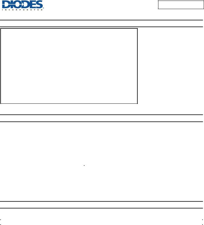
Pin Assignments
( Top View )
IN+ |
1 |
5 |
CC |
|
V |
||
VEE |
2 |
+ |
|
- |
|
||
|
|
|
|
IN- |
3 |
4 |
OUT |
SOT25/SOT353
(Top View)
1OUT |
1 |
|
|
8 |
VCC |
1IN- |
2 |
- |
1 |
7 |
2OUT |
|
|
|
|
|
|
1IN+ |
3 |
+ |
- |
6 |
2IN- |
|
|
|
2 |
|
|
VEE |
4 |
|
+ |
5 |
2IN+ |
|
|
||||
|
|
SO-8/MSOP-8 |
|
|
|
Applications
Mobile Communications
Battery Powered Devices
Notebooks and PDA’s
General Purpose Low-Voltage Applications
General Purpose Portable Devices
Notes: |
1. |
No purposely added lead. Fully EU Directive 2002/95/EC (RoHS) & 2011/65/EU (RoHS 2) compliant. |
|
2. |
See http://www.diodes.com/quality/lead_free.html for more information about Diodes Incorporated’s definitions of Halogenand Antimony-free, "Green" |
|
|
and Lead-free. |
|
3. |
Halogenand Antimony-free "Green” products are defined as those which contain <900ppm bromine, <900ppm chlorine (<1500ppm total Br + Cl) and |
|
|
<1000ppm antimony compounds. |
Schematic Diagram
IN- |
IN+ |
VEE |
|
Each Comparator |
LMV331/ LMV393 |
1 of 13 |
Document number: DS37022 Rev. 2 - 2 |
www.diodes.com |
VCC
OUTPUT
August 2015
© Diodes Incorporated
ADVANCED INFORMATION
LMV331/ LMV393
Pin Descriptions
LMV331
Pin Name |
Pin # |
Function |
|
|
|
IN+ |
1 |
Non-Inverting Input |
|
|
|
VEE |
2 |
Chip Supply Voltage(Negative)/GND |
IN- |
3 |
Inverting Input |
|
|
|
OUT |
4 |
Output |
|
|
|
VCC |
5 |
Chip Supply Voltage(Positive) |
LMV393 |
|
|
1OUT |
1 |
Channel 1 Output |
1IN- |
2 |
Channel 1 Inverting Input |
1IN+ |
3 |
Channel 1 Non-inverting Input |
VEE |
4 |
Chip Supply Voltage(Negative)/GND |
2IN+ |
5 |
Channel 2 Non-inverting Input |
2IN- |
6 |
Channel 2 Inverting Input |
|
|
|
2OUT |
7 |
Channel 2 Output |
|
|
|
VCC |
8 |
Chip Supply Voltage(Positive) |
Absolute Maximum Ratings (Note 4) (@TA = +25°C, unless otherwise specified.)
Symbol |
Description |
|
Rating |
Unit |
|
|
|
|
|
|
|
ESD HBM |
Human Body Model ESD Protection |
|
6.0 |
KV |
|
ESD MM |
Machine Model ESD Protection |
|
200 |
V |
|
|
|
|
|
|
|
VID |
Differential Input Voltage |
|
±Supply Voltage |
V |
|
VCC -VEE |
Supply Voltage |
|
5.5 |
V |
|
|
|
SOT353 (Note 5) |
371 |
|
|
|
|
|
|
|
|
θJA |
Thermal Resistance Junction-to- |
SOT25 (Note 5) |
204 |
°C/W |
|
Ambient |
SO-8 (Note 5) |
120 |
|||
|
|
||||
|
|
|
|
|
|
|
|
MSOP-8 (Note 5) |
180 |
|
|
|
|
|
|
|
|
TST |
Storage Temperature |
|
-65 to +150 |
°C |
|
TJ |
Maximum Junction Temperature |
|
+150 |
°C |
Notes: |
4. Stresses greater than the 'Absolute Maximum Ratings' specified above, may cause permanent damage to the device. These are stress ratings only; |
|
functional operation of the device at these or any other conditions exceeding those indicated in this specification is not implied. Device reliability may be |
|
effected by exposure to absolute maximum rating conditions for extended periods of time. |
|
5. All numbers are typical, and apply for packages soldered directly onto a PC board in still air. |
Recommended Operating Conditions (@TA = +25°C, unless otherwise specified.)
Symbol |
Description |
Rating |
Unit |
|
|
|
|
VCC -VEE |
Supply Voltage |
2.7 to 5.5 |
V |
TA |
Operating Ambient Temperature Range |
-40 to +125 |
°C |
LMV331/ LMV393 |
2 of 13 |
August 2015 |
Document number: DS37022 Rev. 2 - 2 |
www.diodes.com |
© Diodes Incorporated |

LMV331/ LMV393
|
Electrical Characteristics (Notes 6 & 7) (@TA = +25°C, VEE = 0V, VCM = 0V and RL = 5.1KΩ, unless otherwise specified.) |
|
|||||||||||||
|
|
|
|
|
|
|
|
|
|
|
|
|
|
|
|
|
|
|
|
|
|
|
|
|
|
|
|
|
|
|
|
|
Symbol |
|
Parameter |
Test Conditions |
|
Min |
|
Typ |
|
Max |
|
Unit |
|||
|
|
|
|
|
|
|
|
|
|
|
|
|
|
||
|
2.7V DC Electrical Characteristics |
|
|
|
|
|
|
|
|
|
|||||
|
VOS |
|
|
Input Offset Voltage |
- |
- |
1.7 |
7 |
|
mV |
|||||
INFORMATION |
TCVOS |
|
Input Offset Voltage Average Drift |
TA = full range |
- |
5 |
- |
|
µV/°C |
||||||
|
|
|
|
|
|
- |
- |
0.003 |
- |
|
|
||||
|
IB |
|
|
Input Bias Current |
- |
- |
10 |
250 |
|
nA |
|||||
|
|
|
|
|
|
|
TA = full range |
- |
- |
400 |
|
|
|||
|
IOS |
|
|
Input Offset Current |
- |
- |
5 |
50 |
|
nA |
|||||
|
|
|
|
|
|
|
TA = full range |
- |
- |
150 |
|
|
|||
|
VCM |
|
|
Common-Mode Input Voltage Range |
- |
-0.1 |
- |
+2.0 |
|
V |
|||||
|
VSAT |
|
|
Saturation Voltage |
ISINK ≤ 1mA |
- |
120 |
- |
|
mV |
|||||
|
IO |
|
|
Output Sink Current |
VO≤ 1.5V |
5 |
23 |
- |
|
mA |
|||||
|
IOL |
|
|
Output Leakage Current |
|
|
|
|
|
|
|
|
µA |
||
ADVANCED |
|
|
TA = full range |
- |
- |
1 |
|
||||||||
|
|
|
|
|
|
|
|
||||||||
|
|
|
|
LMV331 |
- |
- |
40 |
100 |
|
µA |
|||||
|
|
|
|
|
|
||||||||||
|
IS |
|
|
Supply Current |
|
|
|
|
|
|
|
|
|
|
|
|
|
|
LMV393 |
- |
- |
70 |
150 |
|
uA |
||||||
|
|
|
|
|
(Both Comparators) |
|
|||||||||
|
|
|
|
|
|
|
|
|
|
|
|
|
|
||
|
|
|
|
|
|
|
|
|
|
|
|
|
|
||
|
2.7V AC Electrical Characteristics |
|
|
|
|
|
|
|
|
|
|||||
|
|
|
|
|
|
|
|
|
|
|
|
|
|
|
|
|
tPHL |
|
|
Propagation delay high to low |
Input overdrive= 10mV |
- |
1,000 |
- |
|
ns |
|||||
|
|
|
Input overdrive= 100mV |
- |
350 |
- |
|
ns |
|||||||
|
|
|
|
|
|
|
|
||||||||
|
|
|
|
|
|
|
|
|
|
|
|
|
|
|
|
|
tPLH |
|
|
Propagation delay low to high |
Input overdrive= 10mV |
- |
500 |
- |
|
ns |
|||||
|
|
|
|
|
|
|
|
|
|
|
|
||||
|
|
|
Input overdrive= 100mV |
- |
400 |
- |
|
ns |
|||||||
|
|
|
|
|
|
|
|
||||||||
|
|
|
|
|
|
|
|
|
|
|
|
|
|||
|
5V DC Electrical Characteristics |
|
|
|
|
|
|
|
|
|
|||||
|
|
|
|
|
|
|
|
|
|
|
|
|
|
|
|
|
VOS |
|
|
Input Offset Voltage |
- |
|
- |
|
1.7 |
|
7 |
|
mV |
||
|
|
|
TA = full range |
|
- |
|
- |
|
9 |
|
|||||
|
|
|
|
|
|
|
|
|
|
|
|
||||
|
TCVOS |
|
Input Offset Voltage Average Drift |
TA = full range |
|
- |
|
5 |
|
- |
|
µV/°C |
|||
|
IB |
|
|
Input Bias Current |
- |
|
- |
|
25 |
|
250 |
|
nA |
||
|
|
|
TA = full range |
|
- |
|
- |
|
400 |
|
|||||
|
|
|
|
|
|
|
|
|
|
|
|
||||
|
IOS |
|
|
Input Offset Current |
- |
|
- |
|
2 |
|
50 |
|
nA |
||
|
|
|
|
|
|
|
|
|
|
|
|
||||
|
|
|
TA = full range |
|
- |
|
- |
|
150 |
|
|
||||
|
|
|
|
|
|
|
|
|
|
|
|
||||
|
VCM |
|
|
Common-Mode Input Voltage Range |
- |
|
-0.1 |
|
- |
|
4.2 |
|
V |
||
|
AV |
|
|
Large Signal Differential Voltage Gain |
- |
|
20 |
|
50 |
|
- |
|
V/mV |
||
|
|
|
|
|
|
|
ISINK ≤ 4mA |
|
- |
|
200 |
|
400 |
|
mV |
|
VSAT |
|
|
Saturation Voltage |
ISINK ≤ 4mA, TA = full |
|
- |
|
- |
|
700 |
|
|
||
|
|
|
|
|
|
|
range |
|
|
|
|
|
|||
|
|
|
|
|
|
|
|
|
|
|
|
|
|
|
|
|
|
|
|
|
|
|
|
|
|
|
|
|
|
|
|
|
IO |
|
|
Output Sink Current |
VO≤ 1.5V |
|
10 |
|
84 |
|
- |
|
mA |
||
|
IOL |
|
|
Output Leakage Current |
- |
|
- |
|
0.003 |
|
- |
|
µA |
||
|
|
|
|
|
|
|
|
|
|
|
|||||
|
|
|
TA = full range |
|
- |
|
- |
|
1 |
|
|||||
|
|
|
|
|
|
|
|
|
|
|
|
||||
|
|
|
|
|
|
LMV331 |
- |
|
- |
|
60 |
|
120 |
|
µA |
|
IS |
|
|
Supply Current |
TA = full range |
|
- |
|
- |
|
150 |
|
|||
|
|
|
|
|
|
|
|
|
|||||||
|
|
|
LMV393 |
- |
|
- |
|
100 |
|
200 |
|
uA |
|||
|
|
|
|
|
|
|
|
|
|
||||||
|
|
|
|
|
|
(Both Comparators) |
TA=full range |
|
- |
|
- |
|
250 |
|
|
|
|
|
|
|
|
|
|
|
|
|
|||||
|
5VAC Electrical Characteristics |
|
|
|
|
|
|
|
|
|
|||||
|
tPHL |
|
|
Propagation delay high to low |
Input overdrive = 10mV |
|
- |
|
600 |
|
- |
|
ns |
||
|
|
|
|
|
|
|
|
|
|
|
|
||||
|
|
|
Input overdrive = 100mV |
|
- |
|
200 |
|
- |
|
ns |
||||
|
|
|
|
|
|
|
|
|
|
|
|||||
|
tPLH |
|
|
Propagation delay low to high |
Input overdrive = 10mV |
|
- |
|
450 |
|
- |
|
ns |
||
|
|
|
Input overdrive = 100mV |
|
- |
|
300 |
|
- |
|
ns |
||||
|
|
|
|
|
|
|
|
|
|
|
|||||
|
|
|
|
|
|
|
|
|
|||||||
|
Notes: |
6. Typical values represent the most likely parametric norm as determined at the time of characterization. Actual typical values may vary over time and will |
|||||||||||||
|
|
|
also depend on the application and configuration. The typical values are not tested and are not guaranteed on shipped production material. |
|
|||||||||||
|
|
7. All limits are guaranteed by testing or statistical analysis. |
|
|
|
|
|
|
|
|
|||||
LMV331/ LMV393 |
3 of 13 |
August 2015 |
Document number: DS37022 Rev. 2 - 2 |
www.diodes.com |
© Diodes Incorporated |

ADVANCED INFORMATION
LMV331/ LMV393
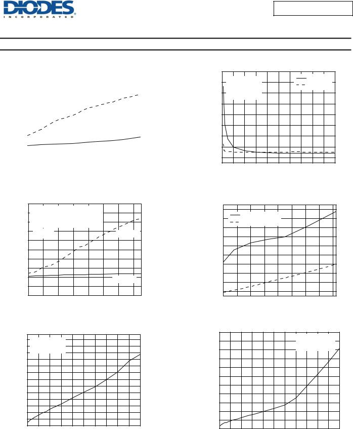
Typical Performance Characteristics (@TA = +25°C, unless otherwise specified.)
|
60 |
|
|
|
|
|
|
55 |
|
|
|
|
|
|
50 |
|
|
|
|
|
|
45 |
|
|
|
|
|
A) |
40 |
|
|
|
o |
|
|
|
|
|
TA=-40 C |
|
|
( |
|
|
|
|
|
|
35 |
|
|
|
TA=25oC |
|
|
Current |
|
|
|
|
||
30 |
|
|
|
TA=85oC |
|
|
25 |
|
|
|
|
|
|
Supply |
|
|
|
|
|
|
20 |
|
|
|
|
|
|
15 |
|
|
|
|
|
|
|
|
|
|
|
|
|
|
10 |
|
|
|
Output High |
|
|
|
|
|
|
|
|
|
5 |
|
|
|
|
|
|
0 |
|
|
|
|
|
|
1 |
2 |
3 |
4 |
5 |
6 |
Supply Voltage (V)
Supply Current vs. Supply Voltage (LMV331)
|
100 |
|
|
|
|
|
|
90 |
TA=-40oC |
|
|
|
|
|
80 |
TA=25oC |
|
|
|
|
|
70 |
TA=85oC |
|
|
|
|
( A) |
|
|
|
|
|
|
60 |
|
|
|
|
|
|
Current |
50 |
|
|
|
|
|
40 |
|
|
|
|
|
|
Supply |
|
|
|
|
|
|
30 |
|
|
|
|
|
|
|
|
|
|
|
|
|
|
20 |
|
|
|
|
|
|
10 |
|
|
|
Output Low |
|
|
|
|
|
|
|
|
|
0 |
|
|
|
|
|
|
1 |
2 |
3 |
4 |
5 |
6 |
Supply Voltage (V)
Supply Current vs. Supply Voltage (LMV331)
|
80 |
|
|
75 |
VCC=5V, VEE=0V |
|
70 |
|
( A) |
65 |
|
60 |
|
|
Current |
|
|
55 |
|
|
|
|
|
Supply |
50 |
|
45 |
|
|
|
|
40Output High Output Low
35 |
|
|
|
|
|
|
|
|
-40 |
-20 |
0 |
20 |
40 |
60 |
80 |
100 |
120 |
Temperature (OC)
Supply Current vs. Temperature (LMV331)
|
75 |
|
|
|
|
|
|
|
|
|
70 |
|
|
|
|
VCC=2.7V, VEE=0V |
|
||
|
|
|
|
|
|
|
|
|
|
|
65 |
|
|
|
|
|
|
|
|
( A) |
60 |
|
|
|
|
|
|
|
|
|
|
|
|
|
|
|
|
|
|
Current |
55 |
|
|
|
|
|
|
|
|
|
|
|
|
|
|
|
|
|
|
Supply |
50 |
|
|
|
|
|
|
|
|
45 |
|
|
|
|
|
|
|
|
|
|
|
|
|
|
|
|
|
|
|
|
40 |
|
Output High |
|
|
|
|
|
|
|
|
|
Output Low |
|
|
|
|
|
|
|
35 |
|
|
|
|
|
|
|
|
|
-40 |
-20 |
0 |
20 |
40 |
60 |
80 |
100 |
120 |
Temperature (OC)
Supply Current vs. Temperature (LMV331)
|
160 |
|
|
|
|
|
|
|
|
|
150 |
|
|
|
|
|
VCC=5V, VEE=0V |
|
|
|
140 |
|
|
|
|
|
|
|
|
|
130 |
|
|
|
|
|
|
|
|
A) |
120 |
|
|
|
|
|
|
|
|
( |
110 |
|
|
|
|
|
|
|
|
Current |
|
|
|
|
|
|
|
|
|
100 |
|
|
|
|
|
|
|
|
|
90 |
|
|
|
|
|
|
|
|
|
Supply |
|
|
|
|
|
|
|
|
|
80 |
|
|
|
|
|
|
|
|
|
70 |
|
|
|
|
|
|
|
|
|
|
60 |
|
Output High |
|
|
|
|
|
|
|
50 |
|
Output Low |
|
|
|
|
|
|
|
40 |
|
|
|
|
|
|
|
|
|
-40 |
-20 |
0 |
20 |
40 |
60 |
80 |
100 |
120 |
Tempareture (oC)
Supply Current vs. Temperature (LMV393)
|
160 |
|
|
|
|
VCC=2.7V, VEE=0V |
|
||
|
150 |
|
|
|
|
|
|||
|
|
|
|
|
|
|
|
|
|
|
140 |
|
|
|
|
|
|
|
|
|
130 |
|
|
|
|
|
|
|
|
A) |
120 |
|
|
|
|
|
|
|
|
110 |
|
|
|
|
|
|
|
|
|
( |
|
|
|
|
|
|
|
|
|
|
|
|
|
|
|
|
|
|
|
Current |
100 |
|
|
|
|
|
|
|
|
90 |
|
|
|
|
|
|
|
|
|
80 |
|
|
|
|
|
|
|
|
|
Supply |
|
|
|
|
|
|
|
|
|
70 |
|
|
|
|
|
|
|
|
|
60 |
|
|
|
|
|
|
|
|
|
|
50 |
|
|
|
|
|
|
|
|
|
40 |
|
Output High |
|
|
|
|
|
|
|
|
|
|
|
|
|
|
||
|
30 |
|
Output Low |
|
|
|
|
|
|
|
20 |
|
|
|
|
|
|
|
|
|
-40 |
-20 |
0 |
20 |
40 |
60 |
80 |
100 |
120 |
Tempareture (oC)
Supply Current vs. Temperature (LMV393)
LMV331/ LMV393 |
4 of 13 |
August 2015 |
Document number: DS37022 Rev. 2 - 2 |
www.diodes.com |
© Diodes Incorporated |
ADVANCED INFORMATION
LMV331/ LMV393
Typical Performance Characteristics (continued) (@ TA = +25°C, unless otherwise specified.)
|
350 |
|
|
|
|
|
|
|
|
|
|
|
|
|
|
|
|
|
|
|
|
|
|
340 |
|
VCC=5V, VEE=0V |
|
|
|
|
|
|
|
|
|
|
|
|
|
|
|
||||
|
|
|
|
|
|
|
|
|
|
|
|
|
|
|
|
|
||||||
|
330 |
|
|
|
|
|
|
|
|
|
|
|
|
|
|
|
|
|||||
|
|
Input Overdrive Voltage=100mV |
|
|
|
|
|
|
|
|||||||||||||
|
320 |
|
|
|
|
|
|
|
|
|||||||||||||
|
|
|
|
|
|
|
|
|
||||||||||||||
|
310 |
|
RL=5.1k |
|
|
|
|
|
|
|
|
|
|
|
|
|
|
|
|
|
||
|
|
|
|
|
|
|
|
|
|
|
|
|
|
|
|
|
|
|
|
|
|
|
(nS) |
300 |
|
|
|
|
|
|
|
|
|
|
|
|
|
|
|
|
|
|
|
|
|
280 |
|
|
|
|
|
|
|
|
|
|
|
|
|
|
|
|
|
|
|
|
|
|
Delay |
290 |
|
|
|
|
|
|
|
|
|
|
|
|
|
|
|
|
|
|
|
|
|
270 |
|
|
|
|
TPLH to 50% |
|
|
|
|
|
|
|
|
|
|
|
|
|||||
|
|
|
|
|
|
|
|
|
|
|
|
|
|
|
|
|
||||||
|
260 |
|
|
|
|
|
|
|
|
|
|
|
|
|
|
|
|
|
|
|
|
|
|
|
|
|
|
|
|
|
|
|
|
|
|
|
|
|
|
|
|
|
|
|
|
Propagation |
250 |
|
|
|
|
|
|
|
|
|
|
|
|
|
|
|
|
|
|
|
|
|
|
|
|
|
|
|
|
|
|
|
|
|
|
|
|
|
|
|
|
|
|
||
200 |
|
|
|
|
|
|
|
|
|
|
|
|
|
|
|
|
|
|
|
|
|
|
|
240 |
|
|
|
|
|
|
|
|
|
|
|
|
|
|
|
|
|
|
|
|
|
|
230 |
|
|
|
|
|
|
|
|
|
|
|
|
|
|
|
|
|
|
|
|
|
|
220 |
|
|
|
|
|
|
|
|
|
|
|
|
|
|
|
|
|
|
|
|
|
|
210 |
|
|
|
|
|
|
|
|
|
TPHL to 50% |
|
|
|
|
|
|
|||||
|
|
|
|
|
|
|
|
|
|
|
|
|
|
|
|
|||||||
|
|
|
|
|
|
|
|
|
|
|
|
|
|
|
|
|
||||||
|
190 |
|
|
|
|
|
|
|
|
|
|
|
|
|
|
|
|
|
|
|
|
|
|
|
|
|
|
|
|
|
|
|
|
|
|
|
|
|
|
|
|
|
|
|
|
|
180 |
|
|
|
|
|
|
|
|
|
|
|
|
|
|
|
|
|
|
|
|
|
|
|
|
|
|
|
|
|
|
|
|
|
|
|
|
|
|
|
|
|
|
|
|
|
170 |
|
|
|
|
|
|
|
|
|
|
|
|
|
|
|
|
|
|
|
|
|
|
|
|
|
|
|
|
|
|
|
|
|
|
|
|
|
|
|
|
|
|
|
|
|
160 |
|
|
|
|
|
|
|
|
|
|
|
|
|
|
|
|
|
|
|
|
|
|
|
|
|
|
|
|
|
|
|
|
|
|
|
|
|
|
|
|
|
|
|
|
|
150 |
|
|
|
|
|
|
|
|
|
|
|
|
|
|
|
|
|
|
|
|
|
|
|
|
|
|
|
|
|
|
|
|
|
|
|
|
|
|
|
|
|
|
|
|
|
-40 |
-20 |
|
0 |
20 |
|
40 |
60 |
80 |
100 |
120 |
|||||||||||
Temperature (oC)
Propagation Delay vs. Temperature
|
1000 |
|
|
|
|
|
|
|
|
900 |
VCC=5V, VEE=0V |
|
|
|
|
|
|
|
|
|
|
|
|
|
|
|
|
|
Input Overdrive Voltage=100mV |
|
|
|
|||
|
800 |
RL=5.1k |
|
|
|
|
|
|
|
|
|
|
|
|
|
|
|
(nS) |
700 |
TA=25OC |
|
|
|
|
TPLH to 50% |
|
|
|
|
|
|
|
|
|
|
Delay |
600 |
|
|
|
|
|
|
|
500 |
|
|
|
|
|
|
|
|
Propagation |
|
|
|
|
|
|
|
|
400 |
|
|
|
|
|
|
|
|
300 |
|
|
|
|
|
|
|
|
|
|
|
|
|
|
|
|
|
|
200 |
|
|
|
|
|
TPHL to 50% |
|
|
|
|
|
|
|
|
||
|
100 |
|
|
|
|
|
|
|
|
0 |
|
|
|
|
|
|
|
|
0 |
20 |
40 |
60 |
80 |
100 |
120 |
140 |
Load Capacitor (pF)
Propagation Delay vs. Load Capacitors
|
2.6 |
VCC=5V, VEE=0V |
|
|
|
|
|
|
|
||
|
|
|
|
|
|
|
|
|
|||
|
2.4 |
TA=25OC |
|
|
|
|
|
|
|
|
|
|
2.2 |
|
|
|
|
|
|
|
|
|
|
|
2.0 |
|
|
|
|
|
|
|
|
|
|
(V) |
1.8 |
|
|
|
|
|
|
|
|
|
|
1.6 |
|
|
|
|
|
|
|
|
|
|
|
Voltage |
|
|
|
|
|
|
|
|
|
|
|
1.4 |
|
|
|
|
|
|
|
|
|
|
|
1.2 |
|
|
|
|
|
|
|
|
|
|
|
Ouput |
1.0 |
|
|
|
|
|
|
|
|
|
|
0.8 |
|
|
|
|
|
|
|
|
|
|
|
|
0.6 |
|
|
|
|
|
|
|
|
|
|
|
0.4 |
|
|
|
|
|
|
|
|
|
|
|
0.2 |
|
|
|
|
|
|
|
|
|
|
|
0.0 |
|
|
|
|
|
|
|
|
|
|
|
0 |
10 |
20 |
30 |
40 |
50 |
60 |
70 |
80 |
90 |
100 |
Output Sink Current (mA)
Output Voltage vs. Output Sink Current
|
4.0 |
|
|
|
|
|
|
|
|
|
|
|
|
|
3.5 |
V |
=5V, V |
|
=0V |
|
|
|
|
TPHL to 50% |
|
||
|
|
CC |
|
EE |
|
|
|
|
|
TPLH to 50% |
|
||
|
|
RL=5.1k |
|
|
|
|
|
|
|
||||
|
|
|
|
|
|
|
|
|
|
|
|||
|
3.0 |
|
|
O |
|
|
|
|
|
|
|
|
|
( S) |
|
TA=25 C |
|
|
|
|
|
|
|
|
|
||
2.5 |
|
|
|
|
|
|
|
|
|
|
|
|
|
Delay |
2.0 |
|
|
|
|
|
|
|
|
|
|
|
|
|
|
|
|
|
|
|
|
|
|
|
|
|
|
Propagation |
1.5 |
|
|
|
|
|
|
|
|
|
|
|
|
1.0 |
|
|
|
|
|
|
|
|
|
|
|
|
|
|
|
|
|
|
|
|
|
|
|
|
|
|
|
|
0.5 |
|
|
|
|
|
|
|
|
|
|
|
|
|
0.0 |
|
|
|
|
|
|
|
|
|
|
|
|
|
|
0 |
20 |
40 |
|
60 |
80 |
100 |
120 |
140 |
160 |
180 |
200 |
Input Overdrive Voltage (mV)
Propagation Delay vs. Input Overdrive Voltage
|
280 |
|
|
|
|
|
|
|
|
|
260 |
|
VCC=5V, ISINK=4mA |
|
|
|
|
||
|
|
VCC=2.7V, ISINK=1mA |
|
|
|
|
|||
|
|
|
|
|
|
|
|||
(mV) |
240 |
|
|
|
|
|
|
|
|
220 |
|
|
|
|
|
|
|
|
|
|
|
|
|
|
|
|
|
|
|
Voltage |
200 |
|
|
|
|
|
|
|
|
180 |
|
|
|
|
|
|
|
|
|
Saturation |
|
|
|
|
|
|
|
|
|
160 |
|
|
|
|
|
|
|
|
|
140 |
|
|
|
|
|
|
|
|
|
|
|
|
|
|
|
|
|
|
|
|
120 |
|
|
|
|
|
|
|
|
|
100 |
|
|
|
|
|
|
|
|
|
-40 |
-20 |
0 |
20 |
40 |
60 |
80 |
100 |
120 |
Temperature (0C)
Saturation Voltage vs. Temperature
|
2.75 |
|
|
|
|
|
|
|
|
|
|
|
|
2.50 |
|
|
|
|
|
|
|
VCC=2.7V, VEE=0 |
|
||
|
|
|
|
|
|
|
|
TA=25OC |
|
|
||
|
2.25 |
|
|
|
|
|
|
|
|
|
||
|
|
|
|
|
|
|
|
|
|
|
|
|
|
2.00 |
|
|
|
|
|
|
|
|
|
|
|
(V) |
1.75 |
|
|
|
|
|
|
|
|
|
|
|
|
|
|
|
|
|
|
|
|
|
|
|
|
Voltage |
1.50 |
|
|
|
|
|
|
|
|
|
|
|
1.25 |
|
|
|
|
|
|
|
|
|
|
|
|
|
|
|
|
|
|
|
|
|
|
|
|
|
Output |
1.00 |
|
|
|
|
|
|
|
|
|
|
|
0.75 |
|
|
|
|
|
|
|
|
|
|
|
|
|
|
|
|
|
|
|
|
|
|
|
|
|
|
0.50 |
|
|
|
|
|
|
|
|
|
|
|
|
0.25 |
|
|
|
|
|
|
|
|
|
|
|
|
0.00 |
|
|
|
|
|
|
|
|
|
|
|
|
0 |
5 |
10 |
15 |
20 |
25 |
30 |
35 |
40 |
45 |
50 |
55 |
Output Sink Current (mA)
Output Voltage vs. Output Sink Current
LMV331/ LMV393 |
5 of 13 |
August 2015 |
Document number: DS37022 Rev. 2 - 2 |
www.diodes.com |
© Diodes Incorporated |
 Loading...