


AP5724FDCG
AP5724
Document number: DS31843 Rev. 4 - 2
1 of 15
www.diodes.com
December 2013
© Diodes Incorporated
A
P5724
WHITE LED STEP-UP CONVERTER
Description
The AP5724 is a step-up DC/DC converter specifically designed to
drive white LEDs with a constant current. The device can drive 2 ~ 6
LEDs in series from a Li-Ion cell. Series connection of the LEDs
provides identical LED currents resulting in uniform brightness and
eliminates the need for ballast resistors. For driving higher number of
LEDs, AP5724 also supports a single feedback of parallel connected
multiple strings of equal number of LEDs.
The AP5724 switches at 1.2MHz that allows the use of tiny external
components. A low 0.1V feedback voltage minimizes power loss in
the current setting resistor for better efficiency
Features
• High Efficiency: 84% Typical
• Fast 1.2MHz Switching Frequency
• Current Limit and UVLO Protections
• Internal Thermal Shutdown
• Internal Over Voltage Protection
• Integrated Soft-Start Function
• SOT26, TSOT26 and U-DFN2020-6: Available in “Green”
Molding Compound (No Br, Sb)
• Lead-Free Finish; RoHS Compliant (Notes 1 & 2)
Pin Assignments
1
2
3
7
4
6
OVP
FB
5
EN
SW
(Top View)
VIN
GND
SOT26 / TSOT23-6
SW
V
IN
OVP
1
2
3
6
5
4
GND
FB
EN
(Top View)
U-DFN2020-6
Applications
• Cellular Phones
• PDAs, Hand held Computers
• Digital Cameras
• MP3 Players
• GPS Receivers
Notes: 1. EU Directive 2002/95/EC (RoHS) & 2011/65/EU (RoHS 2) compliant. All applicable RoHS exemptions applied.
2. See http://www.diodes.com/quality/lead_free.html for more information about Diodes Incorporated’s definitions of Halogen- and Antimony-free, "Green"
and Lead-free.
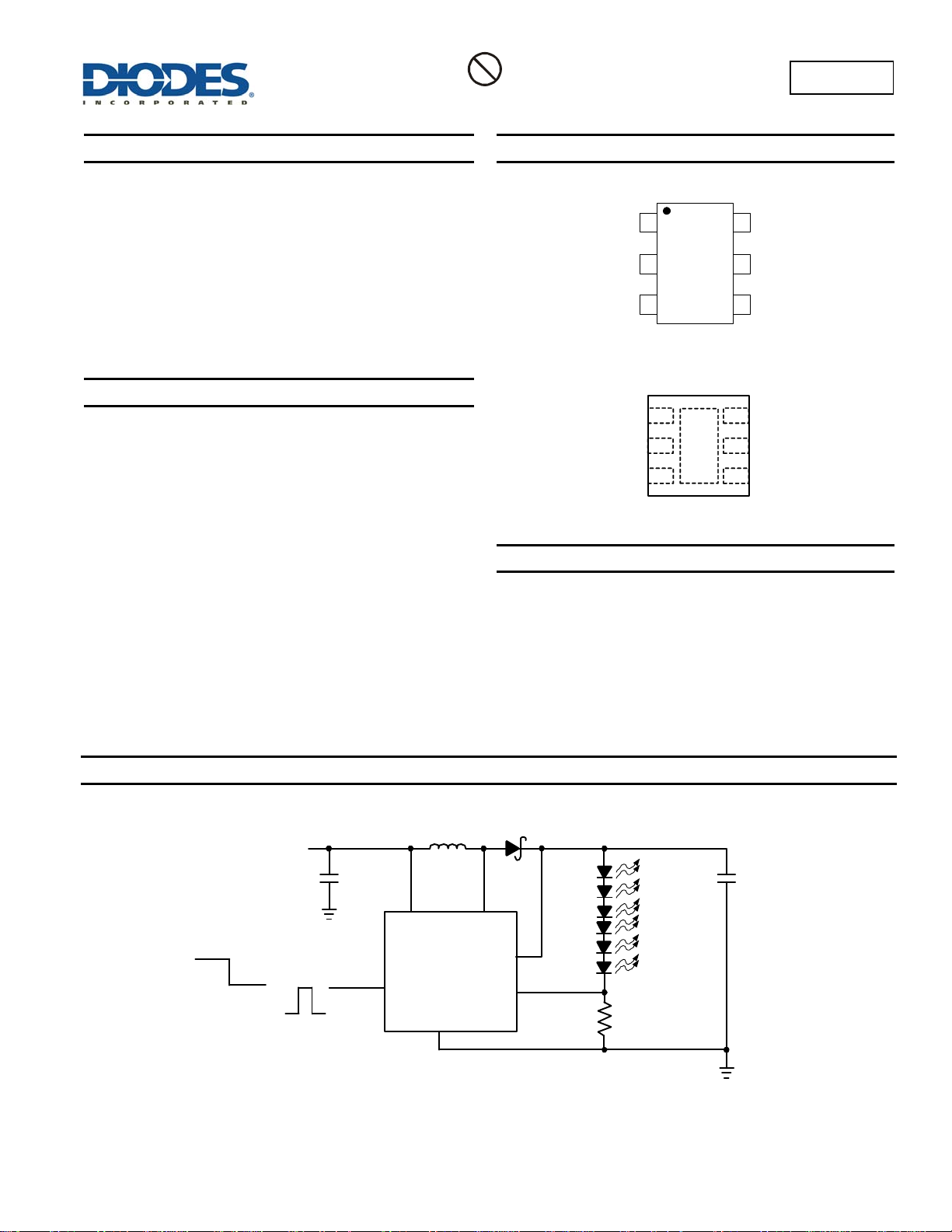
Typical Applications Circuit
V
IN
SW
EN
GND
FB
AP5724
C
OUT
1uF
R
SET
5
L1
22uH
D1
V
IN
C
IN
1uF
OVP
2~6 LEDs
PWM Dimming
OFFON
Figure 1 Typical Application Circuit
Pb
AP5724
Document number: DS31843 Rev. 4 - 2
2 of 15
www.diodes.com
December 2013
© Diodes Incorporated
A
P5724
Pin Descriptions
Pin Name Functions
SW Switch Pin. Connect inductor/diode here. Minimize trace area at this pin to reduce EMI.
GND GND pin.
FB
Feedback Pin. Reference voltage is 0.1V. Connect cathode of lowest LED and a sense resister here. Calculate resistor value
according to the formula: R
SET
= 0.1V / ILED
EN
Converter On/Off Control Input. A high input at EN turns the converter On, and a low input turns it off. If On/Off control is not
needed, connect EN to the input source for automatic startup. The EN pin cannot be left floating.
OVP Output Voltage detect pin for over voltage protection.
V
IN
Input Supply Pin. Must be locally bypassed with 1μF or 2.2μF to reduce input noise.
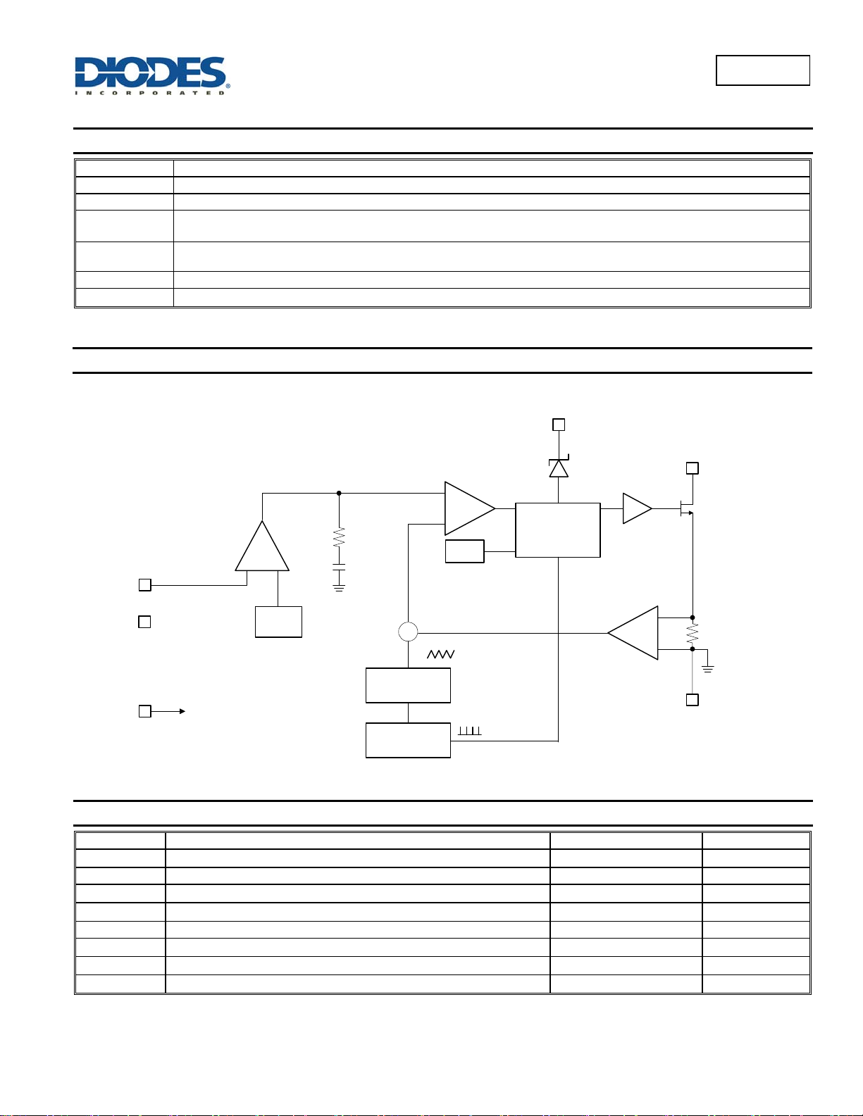
Functional Block Diagram
1.2MHz
Oscillator
RAMP
Generator
Σ
-
+
-
+
-
+
V
REF
0.1V
V
IN
3
FB
Rc
Cc
Comparator
A2
CONTROL
LOGIC
A1
1
Driver
SW
Q1
2
GND
4
EN
Enable
6
OTP
5
OVP
Absolute Maximum Ratings (@T
A
= +25°C, unless otherwise specified.)
Symbol Parameter Rating Unit
V
IN
VIN Pin Voltage -0.3 to +7 V
VSW SW Voltage -0.3 to +34 V
V
OVP
OVP Pin Voltage -0.3 to +35 V
V
FB
Feedback Pin Voltage -0.3 to +7 V
EN EN -0.3 to +7 V
T
J(MAX)
Maximum Junction Temperature 150 °C
T
LEAD
Lead Temperature 300 °C
T
ST
Storage Temperature Range -65 to +150 °C
Caution: Operation above the absolute maximum ratings can cause device failure. These values, therefore, must not be exceeded under any condition.
Operation at the absolute maximum rating for extended periods, may reduce device reliability.
AP5724
Document number: DS31843 Rev. 4 - 2
3 of 15
www.diodes.com
December 2013
© Diodes Incorporated
A
P5724
Recommended Operating Conditions (@T
A
= +25°C, unless otherwise specified.)
Symbol Parameter Min Max Unit
V
IN
Input Voltage 2.7 5.5 V
T
J
Operating Junction Temperature -40 125 °C
T
A
Operating Ambient Temperature -40 85 °C
Electrical Characteristics (@ V
IN
= 3.6V, T
A
= +25°C, unless otherwise specified.)
Symbol Parameter Conditions Min Typ Max Unit
System Supply Input
V
IN
Operating Input Voltage 2.7 — 5.5 V
UVLO Under Voltage Lockout — 2.2 2.4 V
Under Voltage Lockout Hysteretic — 85 — mV
I
Q
Quiescent Current FB = 0.2V, No Switching — 500 — μA
I
SD
Shutdown Current
V
EN
< 0.4V
— 0.1 1 μA
Oscillator
F
OSC
Operation Frequency 1 1.2 1.4 MHz
Dmax Maximum Duty Cycle 86 90 — %
Reference Voltage
V
FB
Feedback Voltage 0.09 0.1 0.11 V
I
FB
FB Pin Bias Current 10 45 100 nA
MOSFET
Rds(on) On Resistance of MOSFET — 0.95 1.2 Ω
I
OCP
Switching Current Limit Normal Operation — 750 — mA
Control and Protection
EN Voltage High ON 1.5 — — V
EN Voltage Low OFF — — 0.4 V
I
EN
EN Pin Pull Low Current — 4 6 μA
OVP OVP Threshold 26 30 34 V
θ
JA
Thermal Resistance Junction-to-Ambient
SOT26 (Note 3) — 162 —
°C/W TSOT26 (Note 3) — 152 —
U-DFN2020-6 (Note 3) — 200 —
θ
JC
Thermal Resistance Junction-to-Case
SOT26 (Note 3) — 36 —
°C/W
TSOT26 (Note 3) — 32 —
U-DFN2020-6 (Note 3) — 30 —
Note: 3. Test condition for SOT26, TSOT26 and U-DFN2020-6: Device mounted on FR-4 substrate, single-layer PC board, 2oz copper, with minimum
recommended pad layout
AP5724
Document number: DS31843 Rev. 4 - 2
4 of 15
www.diodes.com
December 2013
© Diodes Incorporated
A
P5724
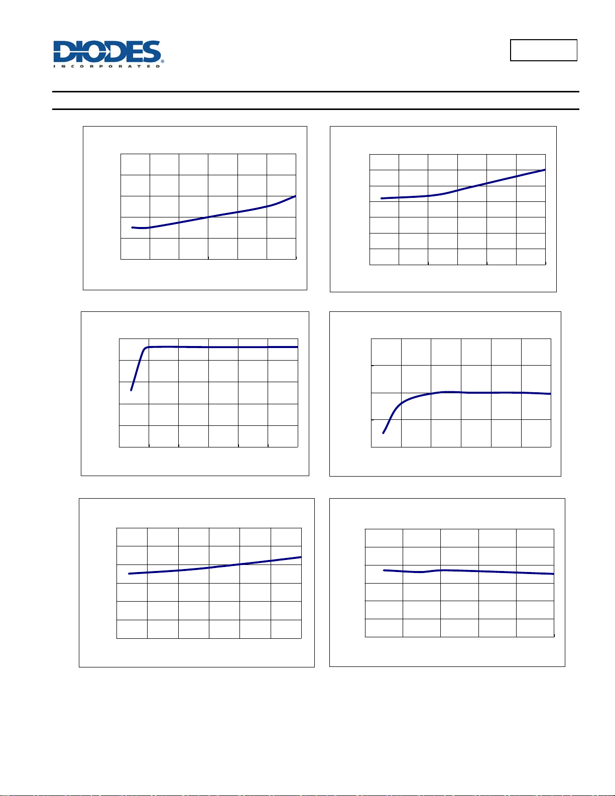
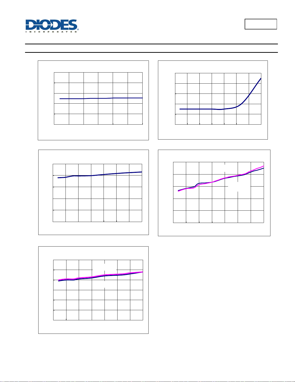
Typical Performance Characteristics (6 LEDS, V
IN
= 3.6V, I
OUT
= 25mA)
V
IN
vs. Shutdown Current
0
0.2
0.4
0.6
0.8
1
2.5 3 3.5 4 4.5 5 5.5
V
IN
(V)
Shutdown Current(uA)
V
IN
vs. Quiescent Current
0
100
200
300
400
500
600
700
2.5 3 3.5 4 4.5 5 5.5
V
IN
(V)
Quiescent Current(uA)
V
IN
vs. Frequency
1
1.05
1.1
1.15
1.2
1.25
2.5 3 3.5 4 4.5 5 5.5
V
IN
(V)
Frequency(MHz)
V
IN
vs. Max Duty
80
85
90
95
100
2.533.544.555.5
V
IN
(V)
Max Duty(%)
V
IN
vs. Feedback Voltage
0.06
0.07
0.08
0.09
0.1
0.11
0.12
2.5 3 3.5 4 4.5 5 5.5
V
IN
(V)
Feedback Voltage(V)
I
OUT
vs. Feedback Voltage
0.06
0.07
0.08
0.09
0.1
0.11
0.12
0 1020304050
I
OUT
(mA)
Feedback Voltage(V)
AP5724
Document number: DS31843 Rev. 4 - 2
5 of 15
www.diodes.com
December 2013
© Diodes Incorporated
A
P5724
Typical Performance Characteristics (cont.) (6 LEDS, V
IN
= 3.6V, I
OUT
= 25mA)
V
IN
vs. OVP Threshold
25
27
29
31
33
35
2.5 3 3. 5 4 4. 5 5 5.5
V
IN
(V)
OVP Threshold(V)
Temperature vs. Shutdown Current
0
0.2
0.4
0.6
0.8
1
-50 -25 0 25 50 75 100 125
Shutdown Current(uA)
Temperature (
℃
)
Temperature vs. OVP Threshold
10
15
20
25
30
35
-50 -25 0 25 50 75 100 125
Temperature (
℃
)
OVP Threshold(V)
Tem perature vs. Frequency
0.2
0.5
0.8
1.1
1.4
1.7
-50 -25 0 25 50 75 100 125
Temperature (
℃
)
Frequency (MHZ)
V
IN
= 3.6V
V
IN
= 4.2V
Temperature vs. Feedback Voltage
60
70
80
90
100
110
120
-50 -25 0 25 50 75 100 125
Temperature (
℃
)
Feedback Voltage(mV)
V
IN
= 4.2V
V
IN
= 3.6V
 Loading...