


PAM8006A
A
f
15W STEREO CLASS-D AUDIO POWER AMPLIFIER WITH POWER LIMIT
Description
The PAM8006A is a 15W (per channel) stereo Class-D audio
amplifier which offers low THD+N (0.2%), low EMI and good PSRR
thus high quality sound reproduction.
The PAM8006A runs off of an 8V to 18V supply at much higher
efficiency than competitors’ Ics.
The PAM8006A only requires very few external components,
significantly saving cost and board space.
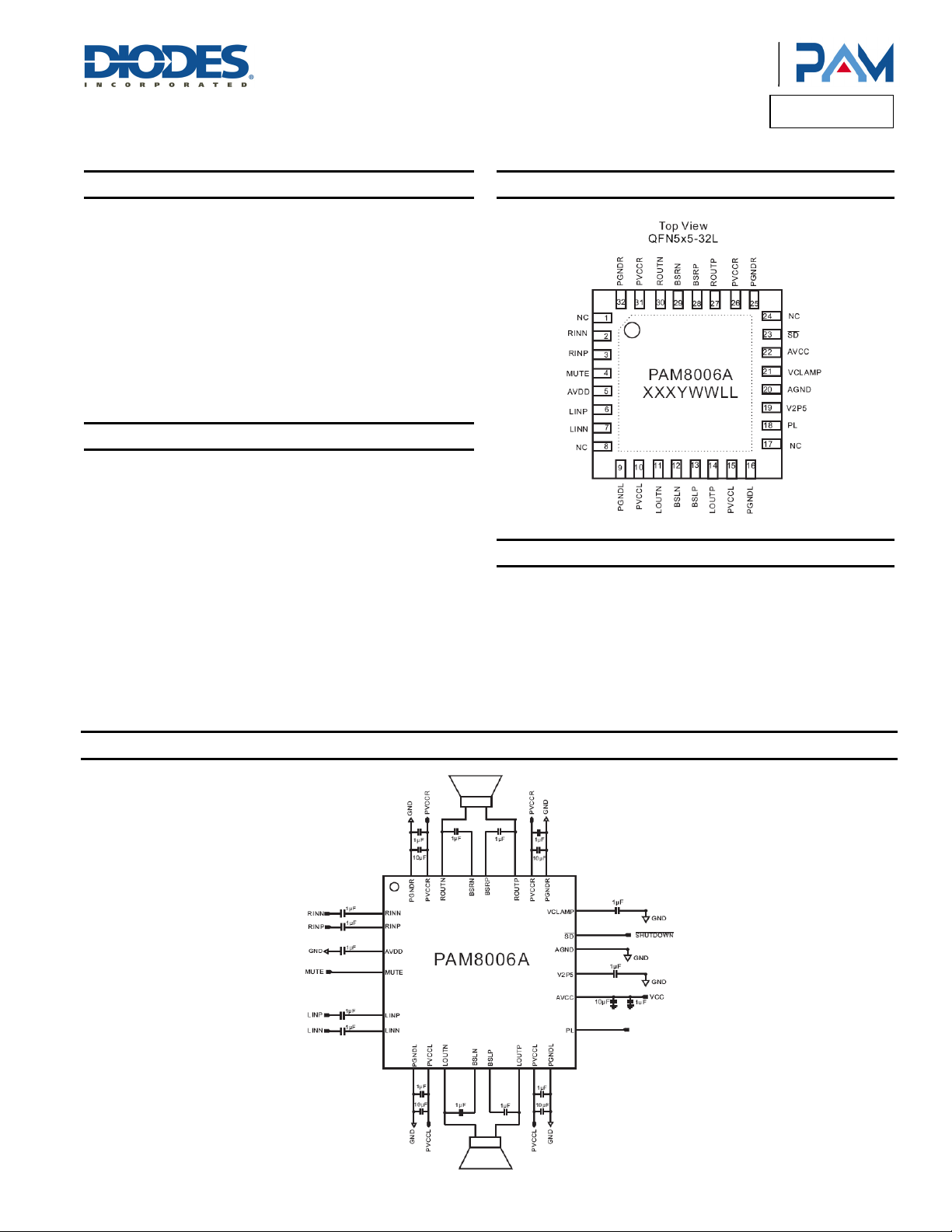
The PAM8006A is available in a QFN5x5-32L package.
Features
Pin Assignments
Product Line o
Diodes Incorporated
PAM8006A
15W x2 into a 8 speaker
Low Noise: -90dB
Over 90% Efficiency
With Shutdown/Mute Function
Over Current ,OVP,UVLO,Thermal and Short-Circuit Protection
Low THD+N
Power Limit with Non-Clip
Low Quiescent Current
Pop Noise Suppression
Small Package Outlines: QFN5x5-32L
Pb-Free Package (RoHS Compliant)
Typical Applications Circuit
Applications
Flat Monitor /LCD TVs
Multi-Media Speaker System
DVD Players, Game Machines
Boom Box
Music Instruments
PAM8006A
Document number: DSxxxxx Rev. 1 - 0
1 of 13
www.diodes.com
April 2013
© Diodes Incorporated
A
f
Product Line o
Diodes Incorporated
PAM8006A
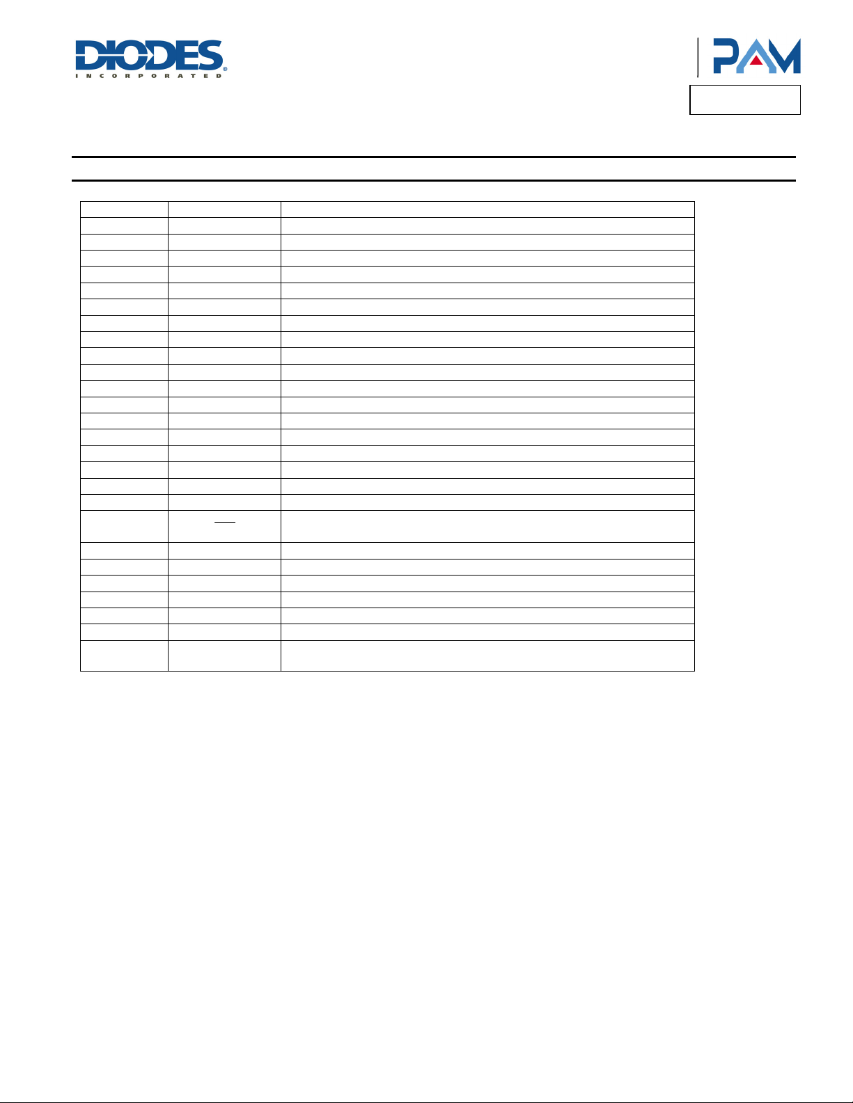
Pin Descriptions
Pin Number Package Name Function
1, 8, 17, 24 NC Not Connected
2 RINN Negative differential audio input for right channel.
3 RINP Positive differential audio input for right channel.
4 MUTE A logic high on this pin disables the outputs and a logic low enables the outputs.
5 AVDD 5V Analog Supply
6 LINP Positive differential audio input for left channel.
7 LINN Negative differential audio input for left channel.
9, 16 PGNDL Power ground for left channel H-bridge.
10, 15 PVCCL Power supply for left channel H-bridge, not connected to PVCCR or AVCC.
11 LOUTN Class-D 1/2-H-bridge negative output for left channel.
12 BSLN Bootstrap I/O for left channel, negative high-side FET.
13 BSLP Bootstrap I/O for left channel, positive high-side FET.
14 LOUTP Class-D 1/2-H-bridge positive output for left channel.
18 PL Reference voltage for power limit function.
19 V2P5 2.5V Reference for analog cells.
20 AGND Analog Ground
21 VCLAMP Internally generated voltage supply for bootstrap capacitors.
22 AVCC High-voltage analog power supply (8V to 26V)
23
25, 32 PGNDR Power ground for right channel H-bridge.
26, 31 PVCCR Power supply for right channel H-bridge, not connected to PVCCL or AVCC.
27 ROUTP Class-D 1/2-H-bridge positive output for right channel.
28 BSRP Bootstrap I/O for right channel, positive high-side FET.
29 BSRN Bootstrap I/O for right channel, negative high-side FET.
30 ROUTN Class-D 1/2-H-bridge negative output for right channel.
33 Thermal Pad
PAM8006A
Document number: DSxxxxx Rev. 1 - 0
SD
Shutdown signal for IC (low= shutdown, high = operational). TTL logic levels
with compliance to V
Connect to ground. Thermal pad should be soldered down on all
applications to secure the device properly to the printed wiring board.
.
CC
2 of 13
www.diodes.com
April 2013
© Diodes Incorporated
A
f
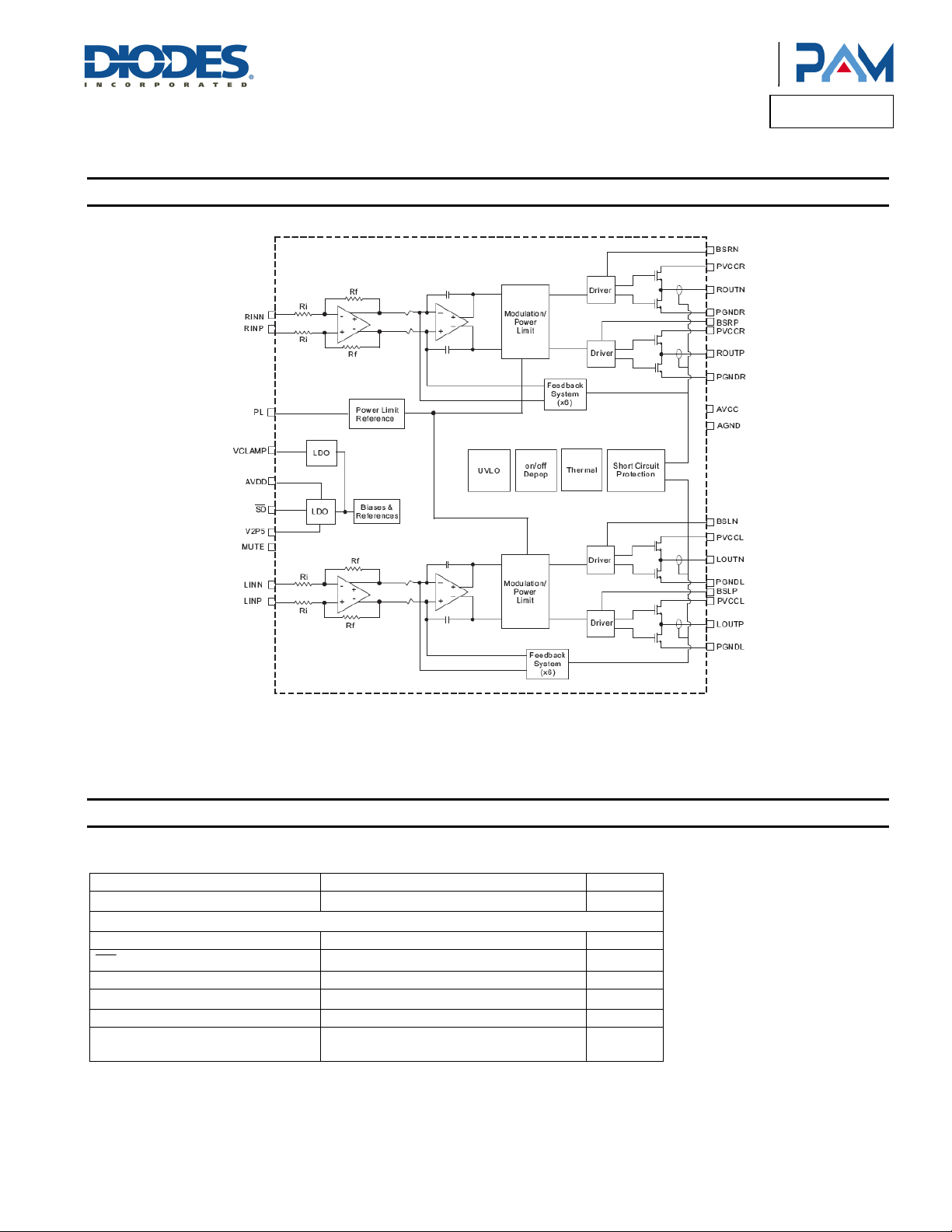
Functional Block Diagram
Product Line o
Diodes Incorporated
PAM8006A
April 2013
© Diodes Incorporated
CC
3 of 13
V
Notes: Maximum Gain: RI = 12.5k, RF = 100k;
Power Limit Function: R
Absolute Maximum Ratings (@T
These are stress ratings only and functional operation is not implied. Exposure to absolute maximum ratings for prolonged time periods may affect device reliability. All
voltages are with respect to ground.
Parameter Rating Unit
Supply Voltage VCC
Input Voltage Range VI:
MUTE, PL 0 to 6.0 V
SD
RINN, RINP, LINN, LINP -0.3 to +6.0 V
Junction Temperature Range, TJ
Storage Temperature -65 to +150 °C
Lead Temperature 1,
6mm (1/16inch)
PAM8006A
Document number: DSxxxxx Rev. 1 - 0
and RF are adjustable.
I
= +25°C, unless otherwise specified.)
A
-0.3 to +28.0 V
-0.3 to V
-40 to +125 °C
260 (5sec) °C
www.diodes.com
A
f
Product Line o
Diodes Incorporated
PAM8006A
Recommended Operating Conditions (@T
Parameter Rating Unit
Supply Voltage VCC
Input Pin Voltage 0 to 5.5 V
High Level Input Voltage: SD
MUTE 2.0 to 5.5 V
Low Level Input Voltage: SD 0 to 0.3 V
MUTE 0 to 0.3 V
Ambient Operating Temperature -20 to +85 °C
8 to 18 V
2.0 to V
CC
= +25°C, unless otherwise specified.)
A
V
Thermal Information
Parameter Package Symbol Maximum Unit
Thermal Resisitance
(Junction to Case)
Thermal Resistance
(Junction to Ambient)
The exposed PAD must be soldered to a thermal land on the PCB.
Electrical Characteristics (@T
Symbol Parameter Conditions Min Typ Max Units
PO
IDD
ISD
R
DS(ON)
PSRR Power Supply Ripple Rejection Ratio
f
OSC
Vn Output Integrated Noise Floor 20Hz to 22kHz, A-Weighting -100 dB
CS Crosstalk
SNR Signal to Noise Ratio
Gain 32 dB
|VOS|
V2P5 2.5V Bias Voltage No Load 2.5 V
AVDD Internal Analog Supply Voltage
OTS Over Temperature Shutdown 160 °C
OTH Thermal Hysteresis 50 °C
PAM8006A
Document number: DSxxxxx Rev. 1 - 0
Continuous Output Power
Quiescent Current (No Load) 16.5 25 mA
Supply Quiescent Current in Shutdown
Mode
Drain-Source On-State Resisitance
Oscillator frequency 300 kHz
Output Offset Voltage
(measured differentially)
QFN5x5-32L
QFN5x5-32L
= +25°C, VCC = 12V, RL =8, unless otherwise specified.)
A
JC
JA
THD+N = 0.12%, f = 1kHz, R
THD+N = 1%, f = 1kHz, RL = 8
THD+N = 10%, f = 1kHz, RL = 8
Shutdown = 0V 4 10 µA
I
= 0.5A
O
= +25°C
T
J
1V
Ripple, f = 1kHz,
PP
Inputs AC-Coupled to Ground
P
= 3W, RL = 8, f = 1kHz
O
Maximum Output at THD+N < 0.5%,
f = 1kHz
INN and INP Connected Together 30 mV
V
= 8V to 26V
CC
www.diodes.com
High Side 210
Low Side 210
Total 420
4 of 13
= 8
L
5.0
°C/W
16.1
6
8.5
10
-65 dB
-95 dB
90 dB
5 5.5 V
© Diodes Incorporated
W
m
April 2013
 Loading...