


A Product Line of
Diodes Incorporated
PAM8902
30-VPP MONO CLASS-D AUDIO AMPLIFIER FOR PIEZO/CERAMIC SPEAKERS
Description |
|
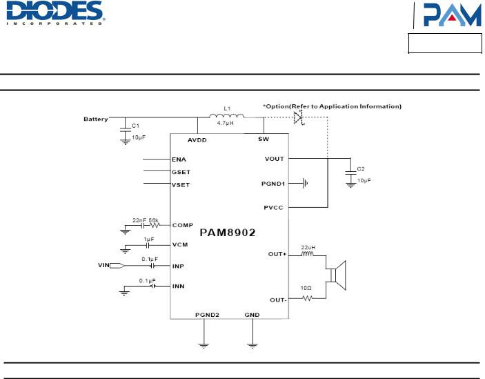
Pin Assignments |
The PAM8902 is a mono, Class-D audio amplifier with integrated boost converter designed for piezo and ceramic speakers.The PAM8902 is capable of driving a ceramic/piezo speaker with 30VPP(10.6Vrms) from a 3.6V power supply.The PAM8902's Boost converter operates at a fixed frequency of 1.5MHz, and provides a 17.5V supply with a minimum number of external components. PAM8902 features an integrated audio low pass filter that rejects high frequency noise thus improving audio fidelity. And three gain modes of 18dB, 22dB and 26dB for ease of use. PAM8902 also provides thermal, short, underand over-voltage protection.
The PAM8902 is available in a 16-ball 1.95mm x 1.95mm CSP package and 16-pin QFN4x4 package.
Features
Supply Voltage Range From 2.5V to 5.5V
30 VPP Output Load Voltage From a 2.5V Supply
Integrated Boost Converter Generates 17.5V Supply
Programmable Soft-Start
Small Boost Converter Inductor
Selectable Gain of 18dB, 22dB, and 26dB
Selectable Boost Output Voltage of 8V, 12V and 17.5V
Low Shutdown Current: < 1µA
Built-in Thermal, OCP, OVP, Short Protection
Available in Space Saving Packages:
16-ball 1.95mmx1.95mm CSP Package
16-pin QFN4x4 Package
Applications
Wireless or Cellular Handsets
Portable DVD Player
Personal Digital Assistants (PDAs )
Electronic Dictionaries
Digital Still Cameras
PAM8902 |
1 of 13 |
November 2012 |
Document number: DSxxxxx Rev. 1 - 4 |
www.diodes.com |
© Diodes Incorporated |
A Product Line of
Diodes Incorporated
PAM8902
Typical Applications Circuit
Pin Descriptions
Pin |
Bump |
Pin Number |
Function |
|
Name |
(CSP) |
QFN4x4 |
||
|
||||
PVCC |
A1 |
16 |
Audio Amplifier Power Supply |
|
VOUT |
A2 |
1 |
Boost Converter Output |
|
SW |
A3 |
2 |
Boost Converter Switching Node |
|
PGND1 |
A4 |
4 |
Boost Converter Power Ground |
|
OUT+ |
B1 |
15 |
Positive Differential Audio Output |
|
VSET |
B2 |
3 |
Boost Converter Output Voltage Setting(8V,12V,17.5V) |
|
COMP |
B3 |
5 |
Boost Converter Compensation |
|
AVDD |
B4 |
6 |
Power Supply |
|
OUT- |
C1 |
14 |
Negative Differential Audio Output |
|
GSET |
C2 |
11 |
Amplifier Gain Setting ( 18dB , 22dB , 26dB) |
|
VCM |
C3 |
7 |
Common Mode Bypass Cap |
|
AGND |
C4 |
8 |
Analog Ground |
|
PGND2 |
D1 |
13 |
ClassD Power Ground |
|
ENA |
D2 |
12 |
Whole Chip Enable |
|
INN |
D3 |
10 |
Negative Differential Audio Input |
|
INP |
D4 |
9 |
Positive Differential Audio Input |
PAM8902 |
2 of 13 |
November 2012 |
Document number: DSxxxxx Rev. 1 - 4 |
www.diodes.com |
© Diodes Incorporated |
A Product Line of
Diodes Incorporated
PAM8902
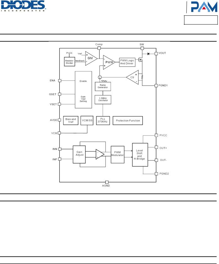
Functional Block Diagram
Absolute Maximum Ratings (@TA = +25°C, unless otherwise specified.)
These are stress ratings only and functional operation is not implied. Exposure to absolute maximum ratings for prolonged time periods may affect device reliability. All voltages are with respect to ground.
Parameter |
Rating |
Unit |
|
Supply Voltage |
6.0 |
V |
|
Input Voltage |
-0.3 to VDD +0.3 |
||
|
|||
Maximum Junction Temperature |
+150 |
|
|
Storage Temperature |
-65 to +150 |
°C |
|
Soldering Temperature |
350, 10sec |
|
Recommended Operating Conditions (@TA = +25°C, unless otherwise specified.)
Parameter |
Rating |
Unit |
Supply Voltage Range |
2.5 to 5.5 |
V |
Ambient Temperature Range |
-40 to +85 |
°C |
Junction Temperature Range |
-40 to +125 |
°C |
PAM8902 |
3 of 13 |
November 2012 |
Document number: DSxxxxx Rev. 1 - 4 |
www.diodes.com |
© Diodes Incorporated |

|
|
|
|
|
|
|
|
|
|
|
A Product Line of |
|
|
|
|
|
||
|
|
|
|
|
|
|
|
|
|
Diodes Incorporated |
|
|
|
|
|
|||
|
|
|
|
|
|
|
|
|
|
|
|
|
|
|
|
|
|
|
|
|
|
|
|
|
|
|
|
|
|
|
|
|
PAM8902 |
|
|||
|
|
|
|
|
|
|
|
|
|
|
|
|
|
|
|
|
|
|
|
Thermal Information |
|
|
|
|
|
|
|
|
|
|
|
|
|
|
|
|
|
|
|
|
|
|
|
|
|
|
|
|
|
|
|
|
|
|
|
|
|
Parameter |
Package |
|
Symbol |
|
Max |
|
Unit |
|
|
|
|
|
|
||||
|
Thermal Resistance (Junction to Ambient) |
CSP |
|
|
θJA |
|
90 |
|
|
|
|
|
|
|
|
|
||
|
QFN4x4-16 |
|
|
52 |
|
°C/W |
|
|
|
|
|
|
||||||
|
|
|
|
|
|
|
|
|
|
|
|
|
||||||
|
Thermal Resistance (Junction to Case) |
CSP |
|
|
θJC |
|
75 |
|
|
|
|
|
|
|
||||
|
|
|
|
|
|
|
|
|
|
|
|
|
||||||
|
QFN4x4-16 |
|
|
30 |
|
|
|
|
|
|
|
|
|
|||||
|
|
|
|
|
|
|
|
|
|
|
|
|
|
|
||||
|
|
|
|
|
|
|
|
|
|
|||||||||
|
Electrical Characteristics (@TA = +25°C, VDD = 3.6V, CL = 1µF, VSET Float, unless otherwise specified.) |
|
|
|
|
|
||||||||||||
|
|
|
|
|
|
|
|
|
|
|
|
|
|
|
|
|||
|
Parameter |
|
Symbol |
|
|
|
Test Conditions |
|
|
Min |
|
Typ |
Max |
Units |
|
|||
|
Input Voltage |
|
VDD |
|
|
|
|
|
|
|
2.5 |
|
|
5.5 |
V |
|
|
|
|
|
|
|
|
EN > 1.2V, VSET = High |
|
|
|
|
30 |
48 |
|
|
|
|
|||
|
Quiescent Current |
|
IQ |
|
EN > 1.2V, VSET = Floating |
|
|
|
|
10 |
18 |
mA |
|
|
|
|||
|
|
|
|
|
EN > 1.2V, VSET = GND |
|
|
|
|
5 |
12 |
|
|
|
|
|||
|
Shutdown Current |
|
ISD |
|
EN = 0V |
|
|
|
|
|
|
0.1 |
1 |
µA |
|
|
|
|
|
Wake-Up Time |
|
TWU |
|
EN from Low to High |
|
|
|
|
40 |
|
mS |
|
|
|
|||
|
Chip Enable |
|
VEH |
|
|
|
|
|
|
|
1.2 |
|
|
|
V |
|
|
|
|
Chip Disable |
|
VEL |
|
|
|
|
|
|
|
|
|
|
0.4 |
|
|
|
|
|
|
|
|
|
|
|
|
|
|
|
|
|
|
|
|
|||
|
GSET/ VSET High |
|
VH |
|
|
|
|
|
|
|
VDD -0.5 |
|
|
VDD |
|
|
|
|
|
GSET/ VSET Floating |
|
VF |
|
|
|
|
|
|
|
1 |
|
|
VDD -1 |
V |
|
|
|
|
GSET/ VSET Low |
|
VL |
|
|
|
|
|
|
|
0 |
|
|
0.5 |
|
|
|
|
|
Under Voltage Lockout Threshold |
|
UVLO |
|
VDD from High to Low |
|
|
|
|
2.2 |
|
V |
|
|
|
|||
|
Under Voltage Lockout Hysteresis |
|
UVLO(H) |
|
VDD from Low to High |
|
|
|
|
0.2 |
|
|
|
|
||||
|
|
|
|
|
|
|
|
|
|
|
|
|||||||
|
Thermal Shutdown Threshold |
|
OTP |
|
|
|
|
|
|
|
|
|
150 |
|
°C |
|
|
|
|
Thermal Shutdown Lockout Hysyeresis |
|
OTP(H) |
|
|
|
|
|
|
|
|
|
30 |
|
°C |
|
|
|
|
|
|
|
|
|
|
|
|
|
|
|
|
|
|
|
|
|
|
|
Boost Converter |
|
|
|
|
|
|
|
|
|
|
|
|
|
|
|
|
|
|
|
|
VO1 |
|
VSET = GND, No Load |
|
|
7.2 |
|
8 |
8.8 |
V |
|
|
|
|||
|
Output Voltage |
|
VO2 |
|
VSET = NC, No Load |
|
|
10.8 |
|
12 |
13.2 |
V |
|
|
|
|||
|
|
|
VO3 |
|
VSET = AVDD, No Load |
|
|
16 |
|
17.5 |
19 |
V |
|
|
|
|||
|
Current Limit |
|
CL |
|
Average Input Current |
|
|
|
|
0.8 |
|
A |
|
|
|
|||
|
Lowside MOSFET RDS(ON) |
|
RLS |
|
IO = 50mA |
|
|
|
|
|
|
0.5 |
|
Ω |
|
|
|
|
|
Boost Switching Frequency |
|
fOSCB |
|
|
|
|
|
|
|
1.1 |
|
1.5 |
1.9 |
MHz |
|
|
|
|
|
|
|
|
|
|
|
|
|
|
|
|
|
|
|
|
|
|
|
Class D |
|
|
|
|
|
|
|
|
|
|
|
|
|
|
|
|
|
|
Class D Amplifier Switching Frequency |
|
fOSCD |
|
Input AC-GND |
|
|
225 |
|
375 |
475 |
KHz |
|
|
|
|||
|
Common Mode Reject Ratio |
|
CMRR |
|
VIN = + -100mV, VDD = 3.6V |
|
|
|
|
60 |
|
dB |
|
|
|
|||
|
Output Offset Voltage |
|
VOS |
|
Output Offset Voltage |
|
|
|
|
5 |
50 |
mV |
|
|
|
|||
|
RDS(ON) |
|
RP |
|
High Side |
|
|
|
|
|
|
1.5 |
|
Ω |
|
|
|
|
|
|
|
Low Side |
|
|
|
|
|
|
0.6 |
|
Ω |
|
|
|
|||
|
|
|
|
|
|
|
|
|
|
|
|
|
||||||
|
|
|
AV1 |
|
GSET = AVDD, VO = 1VRMS |
|
|
25 |
|
26 |
27 |
|
|
|
|
|||
|
Closed-Loop Voltage Gain |
|
AV2 |
|
GSET = NC, VO = 1VRMS |
|
|
21 |
|
22 |
23 |
|
|
|
|
|||
|
|
|
AV3 |
|
GSET = GND, VO = 1VRMS |
|
|
17 |
|
18 |
19 |
dB |
|
|
|
|||
|
Power Supply Reject Ratio |
|
PSRR |
|
200m VPP Supply Ripple @ 217Hz |
|
|
|
70 |
|
dB |
|
|
|
||||
|
Total Harmonic Distortion Plus Noise |
|
THD+N |
|
VO = 5VRMS |
|
|
|
|
0.3 |
|
% |
|
|
|
|||
|
Signal to Noise Ratio |
|
SNR |
|
Input AC Ground, A–Weighting |
|
|
|
90 |
|
dB |
|
|
|
||||
|
PAM8902 |
|
|
|
|
4 of 13 |
|
|
|
|
|
November 2012 |
||||||
|
Document number: DSxxxxx Rev. 1 - 4 |
|
|
www.diodes.com |
|
|
|
|
|
© Diodes Incorporated |
||||||||

A Product Line of
Diodes Incorporated
PAM8902
Typical Performance Characteristics
(@TA = +25°C, VDD = 4.2V, Gain = 26dB, CIN = 1µF, CLOAD = 1µF, unless otherwise specified.)
PAM8902 |
5 of 13 |
November 2012 |
Document number: DSxxxxx Rev. 1 - 4 |
www.diodes.com |
© Diodes Incorporated |
 Loading...