


AP63200
Table of contents
 Loading...
AP63200/AP63201/AP63203/AP63205
is a 2A, synchronous
range of 3.8V to 32V and
down DC/DC
easily used by
minimizing the external component count due to its adoption of peak
The AP63200/AP63201/AP63203/AP63205 has optimized designs for
tion. The converter features
Frequency Spread Spectrum (FSS) with a switching frequency jitter of
reduces EMI by not allowing emitted energy to stay in any
It also has a proprietary
without sacrificing
• Halogen and Antimony Free. “Green” Device (Note 3)
1
2
3 4
5
6
FB
EN
VIN GND
SW
BST
TSOT26
TOP VIEW
3.8V TO 32V INPUT, 2A LOW IQ SYNCHRONOUS BUCK WITH ENHANCED EMI REDUCTION
Description
The AP63200/AP63201/AP63203/AP63205
buck converter with a wide input voltage
fully integrates a 125mΩ high-side power MOSFET and a 68mΩ lowside power MOSFET to provide high-efficiency stepconversion.
The AP63200/AP63201/AP63203/AP63205 device is
Pin Assignments
current mode control along with its integrated compensation network.
Electromagnetic Interference (EMI) reduc
±6%, which
one frequency for a significant period of time.
gate driver scheme to resist switching node ringing
MOSFET turn-on and turn-off times, which further erases highfrequency radiated EMI noise caused by MOSFET switching.
The device is available in a low-profile, TSOT26 package.
Features
• VIN 3.8V to 32V
• 2A Continuous Output Current
• 0.8V ± 1% Reference Voltage
• 22µA Ultralow Quiescent Current
• Switching Frequency
o 500kHz: AP63200 and AP63201
o 1.1MHz: AP63203 and AP63205
• Pulse Width Modulation (PWM) Regardless of Output Load
o AP63201
• Supports Pulse Frequency Modulation (PFM)
o AP63200, AP63203, and AP63205
o Up to 80% Efficiency at 1mA Light Load
o Up to 88% Efficiency at 5mA Light Load
• Fixed Output Voltage
o 3.3V: AP63203
o 5.0V: AP63205
• Proprietary Gate Driver Design for Best EMI Reduction
• Frequency Spread Spectrum (FSS) to Reduce EMI
• Precision Enable Threshold to Adjus t UVLO
• Protection Circuitry
o Overvoltage Protection
o Cycle-by-Cycle Peak Current Limit
o Thermal Shutdown
• Totally Lead-Free & Fully RoHS Compliant (Notes 1 & 2)
Applications
• 12V and 24V Distributed Power Bus Supplies
• Flat Screen TV Sets and Monitors
• Power Tools and Laser Printers
• White Goods and Small Home Appliances
• FPGA, DSP, and ASIC Supplies
• Home Audio
• Network Systems
• Set Top Boxes
• Gaming Consoles
• Consumer Electronics
Notes: 1. No purposely added lead. Fully EU Directive 2002/95/EC (RoHS), 2011/65/EU (RoHS 2) & 2015/863/EU (RoHS 3) compliant.
2. See https://www.diodes.com/quality/lead-free/ for more information about Diodes Incorporated’s definitions of Halogen- and Antimony-free, "Green" and
3. Halogen- and Antimony-free "Green” products are defined as those which contain <900ppm bromine, <900ppm chlorine (<1500ppm total Br + Cl) and
Lead-free.
<1000ppm antimony compounds.
AP63200/AP63201/AP63203/AP63205
Document number: DS41326 Rev. 2 - 2
1 of 18
www.diodes.com
January 2019
© Diodes Incorporated
AP63200/AP63201/AP63203/AP63205
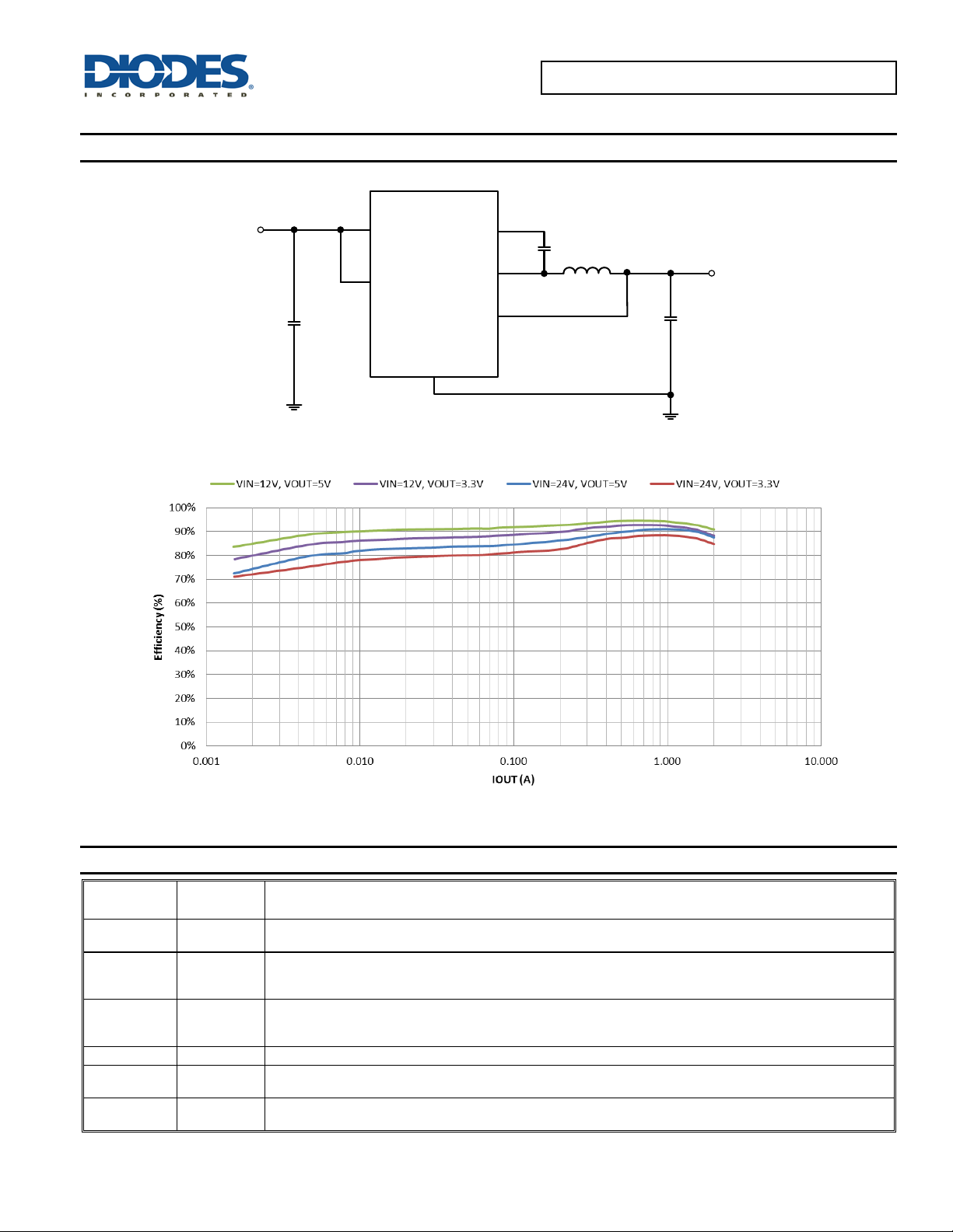
AP63205
L
4.7µH
C3
100nF
C2
2x22μF
C1
10μF
3
VIN
2
EN
5
SW
6
BST
1
FB
4
GND
OUTPUT
V
OUT
5V
INPUT
Feedback sensing terminal for the output voltage. Connect this pin to the resistive divider of the output.
Setting the Output Voltage
programing the UVLO. See Enable section for more details.
Power Input. VIN suppli es the power to the IC, as well as the step-down converter switches. Drive VIN wi th a
switching of the IC. See Input Capacitor section for more details.
4
GND
Power Ground.
Power Switching Output. SW is the switching node that supplies power to the output. Connect the output LC filter
from SW to the output load. Note that a capacitor is required from SW to BST to power the high-side switch.
High-Side Gate Drive Boost Input. BST supplies the drive for the high-side N-Channel MOSFET. A 100nF
Typical Application Circuit
Figure 1. Typical Application Circuit
Figure 2. Efficiency vs. Output Current
Pin Descriptions
Pin Number Pin Name Function
1 FB
2 EN
AP63200/AP63201/AP63203/AP63205
Document number: DS41326 Rev. 2 - 2
3 VIN
5 SW
6 BST
See
section for more details.
Enable Input. EN is a digital input that turns the regulator on or off. Drive EN high to turn on the regulator and low
to turn it off. Attach to VIN or leave open f or automatic startup. The EN has a precision threshold of 1.18V f or
3.8V to 32V power source. Bypass VIN t o GND with a suitably large capacitor to eliminate noise due to the
capacitor is recommended from SW to BST to power the high-side switch.
2 of 18
www.diodes.com
January 2019
© Diodes Incorporated
AP63200/AP63201/AP63203/AP63205
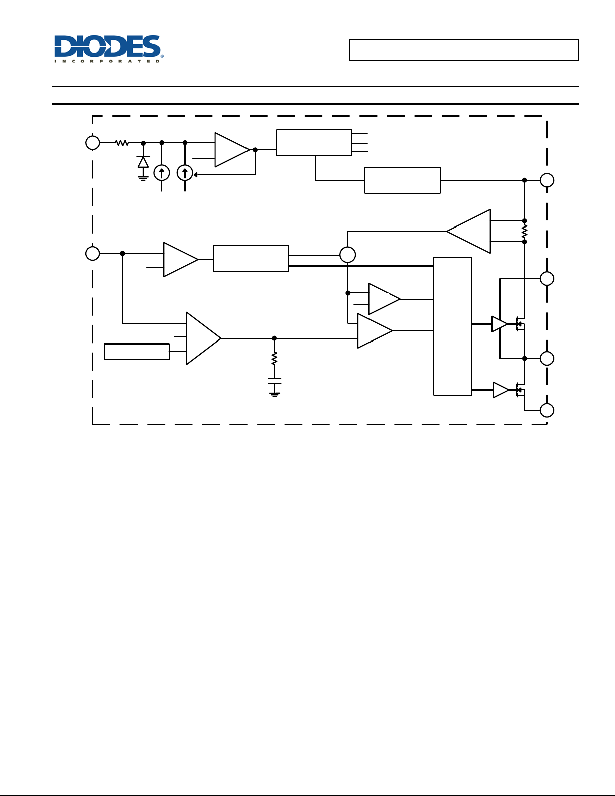
0.4V
0.8V
1.1V
+
-
+
-
-
+
0.6V
+
0.8V
Inte rna l SS
Error
Amplifier
PWM
Comparator
Oscillator
+
Logic
-
+
Ref
OCP
7.6nF
18kΩ
SE = 0.84V/T
RT = 0.2V/A
UVP
Q1
Q2
1
2
EN
FB
4
GND
5
SW
6
BST
3
VIN
gm
20kΩ
+
-
Internal
Reference
VCC
Regulator
ON
1.18V
1.5µA 4µA
VSUM
COMP
CSA
Functional Block Diagram
AP63200/AP63201/AP63203/AP63205
Document number: DS41326 Rev. 2 - 2
Figure 3. Functional Block Diagram
3 of 18
www.diodes.com
January 2019
© Diodes Incorporated
AP63200/AP63201/AP63203/AP63205
Symbol
Parameter
Rating
Unit
IN
BST
SW
SW
Feedback Voltage
-0.3V to +6.0
V
VEN
Enable/UVLO Voltage
-0.3V to +35.0
V
TST
TJ
TL
Lead Temperature
+260
°C
ESD Susceptibility (Note 5)
HBM
Human Body Mode
2000
V
CDM
Charge Device Model
1000
V
Symbol
Parameter
Rating
Unit
θ
JA
θ
JC
Symbol
Parameter
Min
Max
Unit
3.8
Operating Ambient Temperature Range
-40
+85
°C
Absolute Maximum Ratings (Note 4) (@T
= +25°C, unless otherwise specified.)
A
VIN
VSW
V
Supply Voltage
Switch Node Voltage
Bootstrap Voltage
-0.3 to +35.0 (DC) V
-0.3 to +40.0 (400ms) V
V
-1.0 to V
- 0.3 to V
+ 0.3
+ 6.0
V
V
VFB
Storage Temperature -65 to +150 °C
Junction Temperature +160 °C
Notes: 4. Stresses greater than the 'Absolute Maximum Ratings' specified above may cause permanent damage to the device. These are stress ratings only;
functional operation of the device at these or any other conditions exceeding those indicated in this specification is not implied. Device reliability may
be affected by exposure to absolute maximum rating conditions for extended periods of time.
5. Semiconductor devices are ESD sensitive and may be damaged by exposure to ESD events. Suitable ESD precautions should be taken when
handling and transporting these devices.
Thermal Resistance (Note 6)
Junction to Ambient TSOT26 89 °C/W
Junction to Case TSOT26 39 °C/W
Note: 6. Test condition for TSOT26: Device mounted on FR-4 substrate, single-layer PC board, 2oz copper, with minimum recommended pad layout.
Recommended Operating Conditions (Note 7) (@T
= +25°C, unless otherwise specified.)
A
VIN
TA
Note: 7. The device function is not guaranteed outside of the recommended operating conditions.
AP63200/AP63201/AP63203/AP63205
Document number: DS41326 Rev. 2 - 2
Supply Voltage
4 of 18
www.diodes.com
32 V
January 2019
© Diodes Incorporated
AP63200/AP63201/AP63203/AP63205
Symbol
Parameter
Test Conditions
Min
Typ
Max
Unit
I
SHDN
Shutdown Supply Current
VEN = 0V
— 1 3
µA
AP63201:
VEN = OPEN, VFB = 1.0V
AP63200/AP63203/AP63205:
IN
R
DS(ON)1
High-Side Switch On-Resistance (Note 8)
— — 125 — mΩ
R
DS(ON)2
I
PEAK_LIMIT
I
VALLEY_LIMIT
AP63200/AP63201
—
500 — kHz
AP63203/AP63205
—
1100 — kHz
FSS
Frequency Spread Spectrum
— — ±6 — %
tON
CCM, AP63200/AP63201
792
800
808
mV
CCM, AP63203
3.27
3.30
3.33
V
CCM, AP63205
4.95
5.00
5.05
V
V
EN_H
V
EN_L
VEN = 1.5V
VEN = 1V
—
1.5 — μA
tSS
Soft-Start Period
— — 4 — ms
HYS
Electrical Characteristics (T
ambient temperature range, -40°C to +85°C, and input voltage range, 3.8V to 32V).
IQ
UVLO
Supply Current (Quiescent)
V
Under Voltage Threshold (Rising)
VIN Under Voltage Threshold Hysteresis
Low-Side Switch On-Resistance (Note 8) — — 68 — mΩ
HS Peak Current Limit (Note 8) — 2.5 2.8 3.1 A
LS Valley Current Limit (Note 8) — 2.5 3.2 3.9 A
= +25°C, VIN = 12V, unless otherwise specified. Min/Max limits apply across the recommended
A
VEN = OPEN, VFB = 1.0V
— 3.30 3.50 3.70 V
— — 440 — mV
— 258 — µA
— 22 — µA
fSW
Oscillator Frequency
Minimum On Time — — 80 — ns
VFB
Feedback Voltage
EN Logic High — 1.15 1.18 1.23 V
EN Logic Low — 1.05 1.10 1.15 V
IEN
TSD
T
Note: 8. Compliance to the datasheet limits is assured by one or more methods: production test, characterization, and/or design.
EN Input Current
Thermal Shutdown (Note 8) — — +160 — °C
Thermal Hysteresis (Note 8) — — +25 — °C
— 5.5 — μA
AP63200/AP63201/AP63203/AP63205
Document number: DS41326 Rev. 2 - 2
5 of 18
www.diodes.com
January 2019
© Diodes Incorporated

AP63200/AP63201/AP63203/AP63205
Figure 4. Efficiency vs. Output Current, VIN = 12V
Figure 5. Efficiency vs. Output Current, VIN = 24V
Figure 6. Load Regulation, VOUT = 5V
Figure 7. Line Regulation, VOUT = 5V
Figure 8. Feedback Voltage vs. Temperature
Figure 9. Power Switch R
vs. Temperature
Typical Performance Characteristics (AP63200 @T
= +25°C, VIN = 12V, V
A
= 5V, unless otherwise specified.)
OUT
AP63200/AP63201/AP63203/AP63205
Document number: DS41326 Rev. 2 - 2
www.diodes.com
6 of 18
DS(ON)
January 2019
© Diodes Incorporated
Loading...