


AP4310
Data Sheet
DUAL OP AMP AND VOLTAGE REFERENCE AP4310/A
General Description
The AP4310/A is a monolithic IC specifically
designed to regulate the output current and voltage levels of switching battery chargers and power supplies.
The device contains two Op Amps and a 2.5V precision shunt voltage reference. Op Amp 1 is designed for
voltage control with its non-inverting input internally
connected to the output of the shunt regulator. Op
Amp 2 is for current control with both inputs uncommitted. The IC offers the power converter designer a
control solution that features increased precision with a
corresponding reduction in system complexity and
cost. AP4310A has more strigent reference voltage
tolerance than AP4310.
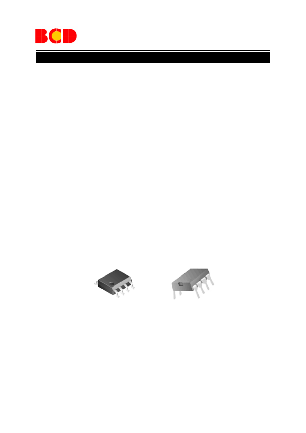
The AP4310/A is available in standard packages of
DIP-8 and SOIC-8.
Features
Op Amp
· Input Offset Voltage: 0.5mV
· Supply Current: 75µA per Op Amp at 5.0V Sup-
ply Voltage
· Unity Gain Bandwidth: 1MHz
· Output Voltage Swing: 0 to (V
· Power Supply Range: 3 to 36V
Voltage Reference
· Fixed Output Voltage Reference: 2.5V
· Reference Voltage Tolerance
AP4310A: ± 0.4%,
AP4310: ± 1%
· Sink Current Capability: 0.05 to 80mA
· Typical Output Impedance: 0.2
CC
Ω
-1.5) V
Applications
· Battery Charger
· Switching Power Supply
SOIC-8 DIP-8
Figure 1. Package Types of AP4310/A
Jan. 2013 Rev. 1. 8 BCD Semiconductor Manufacturing Limited
1
Data Sheet
DUAL OP AMP AND VOLTAGE REFERENCE AP4310/A
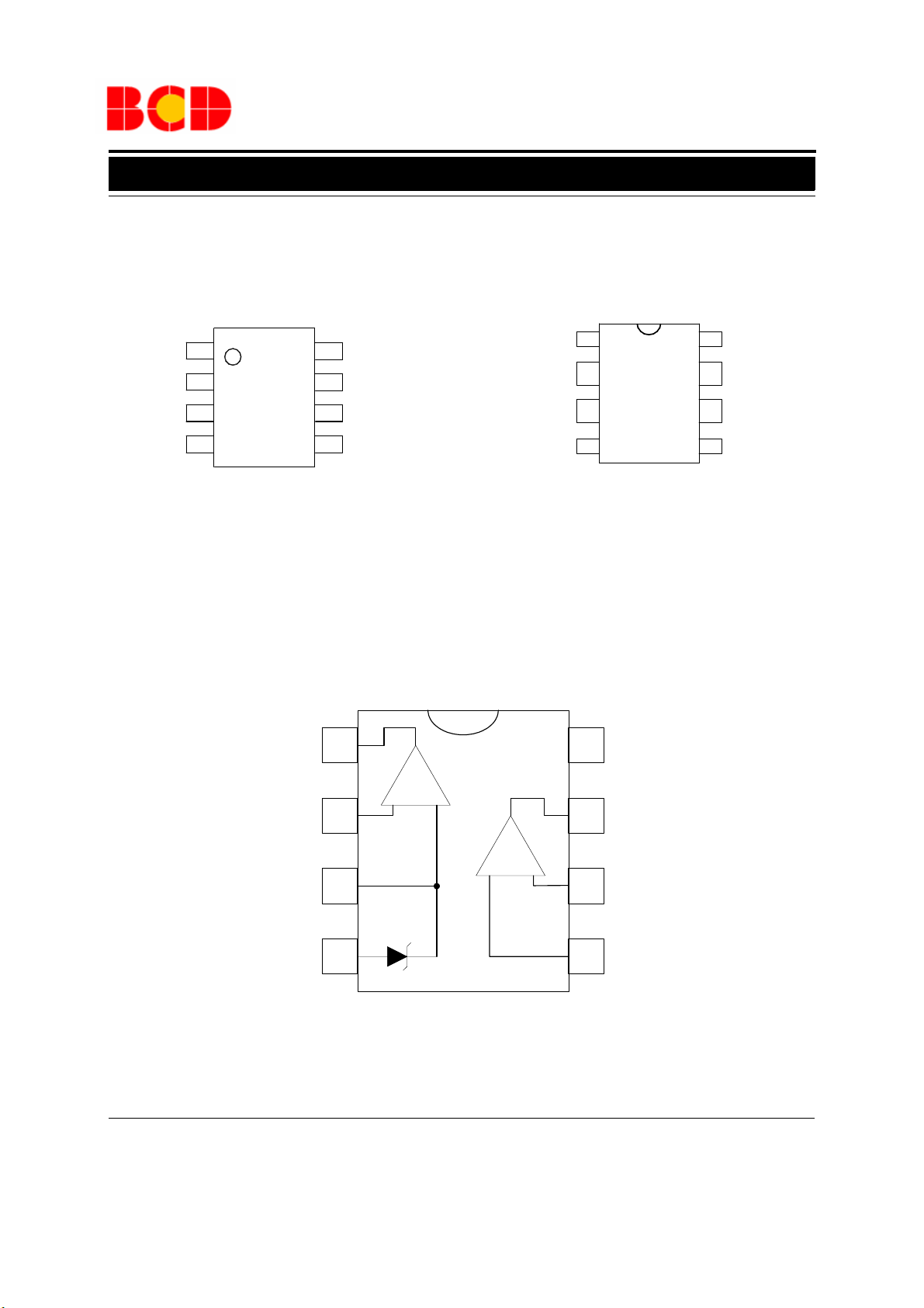
Pin Configuration
M Package
(SOIC-8)
OUTPUT 1
INPUT 1-
INPUT 1+/V
GND
KA
1
2
3
4
Functional Block Diagram
P Package
KA
1
2
3
4
V
8
CC
OUTPUT 2
7
INPUT 2-
6
5
INPUT 2+
Figure 2. Pin Configuration of AP4310/A (Top View)
OUTPUT 1
INPUT 1-
INPUT 1+/V
GND
(DIP-8)
V
8
OUTPUT 2
7
INPUT 2-
6
INPUT 2+
5
CC
OUTPUT 1
1
Op
8
V
CC
Amp 1
-
+
INPUT 1-
INPUT 1+ / V
KA
2
-
+
3
7
6
OUTPUT 2
INPUT 2-
Op
Amp 2
GND
4
Figure 3. Functional Block Diagram of AP4310/A
5
INPUT 2+
Jan. 2013 Rev. 1. 8 BCD Semiconductor Manufacturing Limited
2

Data Sheet
DUAL OP AMP AND VOLTAGE REFERENCE AP4310/A
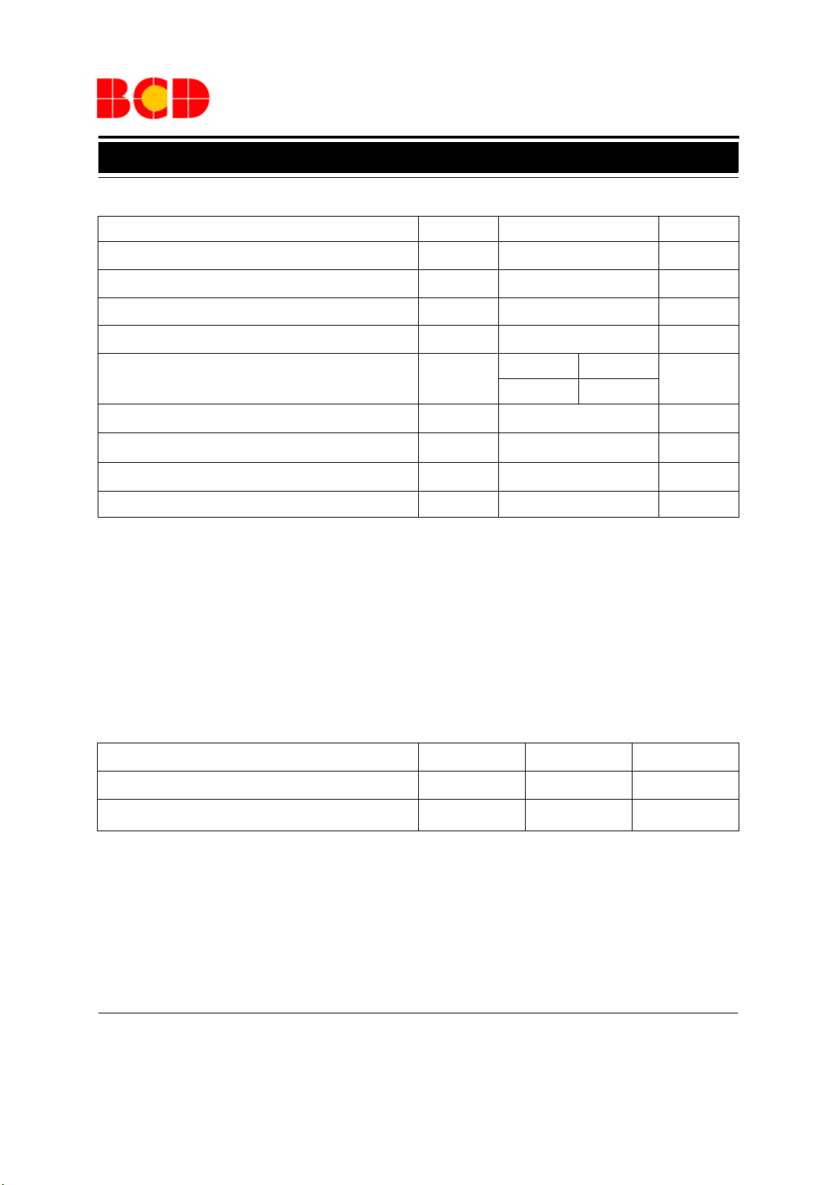
Ordering Information
AP4310 -
G1: Green
Circuit Type
TR: Tape and Reel
Blank: Tube
Blank: AP4310
A: AP4310A
Package
M: SOIC-8
P: DIP-8
Package
DIP-8 2.5V
SOIC-8 2.5V
Reference
Vo lt ag e
Vo lt ag e
To le ra nc e
± 0.4%
± 1% AP4310P-G1 AP4310P-G1
± 0.4%
± 1%
Te mp er at ur e
Range
-40 to 105
-40 to 105
-40 to 105
o
o
o
Part Number Marking ID Packing Type
AP4310AP-G1 AP4310AP-G1
C
AP4310AM-G1 AP4310AM-G1 Tube
C
AP4310AMTR-G1 AP4310AM-G1 Tape & Reel
AP4310M-G1 AP4310M-G1 Tube
C
AP4310MTR-G1 AP4310M-G1 Tape & Reel
BCD Semiconductor's products, as designated with "G1" suffix in the part number, are RoHS compliant and Green.
Tube
Jan. 2013 Rev. 1. 8 BCD Semiconductor Manufacturing Limited
3
Data Sheet
DUAL OP AMP AND VOLTAGE REFERENCE AP4310/A
Absolute Maximum Ratings (Note 1)
Parameter Symbol Value Unit
Power Supply Voltage (V
Op Amp 1 and 2 Input Voltage Range (Pins 2, 5, 6) V
Op Amp 2 Input Differential Voltage (Pins 5, 6) V
Voltage Reference Cathode Current (Pin 3) I
to GND) V
CC
CC
IN
ID
K
40 V
-0.3 to VCC+0.3 V
40 V
100 mA
DIP-8 800
Power Dissipation (T
=25oC)
A
P
D
Operating Junction Temperature T
Storage Temperature Range T
Lead Temperature (Soldering 10s) T
STG
LEAD
ESD (Human Body Model) ESD
SOIC-8 500
J
150
-65 to 150
260
≥ 2000
mW
o
C
o
C
o
C
V
Note 1: Stresses greater than those listed under "Absolute Maximum Ratings" may cause permanent damage to the
device. These are stress ratings only, and functional operation of the device at these or any other conditions
beyond those indicated under "Recommended Operating Conditions" is not implied. Exposure to "Absolute Maximum Ratings" for extended periods may affect device reliability.
Recommended Operating Conditions
Parameter Min Max Unit
Supply Voltage 3 36 V
Ambient Temperature -40 105
Jan. 2013 Rev. 1. 8 BCD Semiconductor Manufacturing Limited
4
o
C
 Loading...