


AP6714
1.8MHz SYNCHRONOUS BOOST CONVERTER
Description
The AP6714 is fully integrated synchronous current mode boost converter which provides a complete power supply solution for all one-cell, two-cell, three cell, alkaline, NiCd or NiMh or single-cell Lithion battery powered products. They improve performance, component count and size compared to conventional controllers, lithium-ion (Li+) designs. On-chip MOSFETs provide up to 94% efficiency for critical power supplies. This optimizes overall efficiency and cost, while also reducing board space. Operate at one fixed frequency of 1.8MHz to optimize size, cost, and efficiency. Other features include soft-start and overload protection. AP6714 is available in space-saving 10-pin MSOP package.
Pin Assignments |
|
|
|
|
( Top View ) |
|
|
Vcc |
1 |
10 |
OUT |
EN |
2 |
9 |
LX |
CC |
3 |
8 |
OCP |
FB |
4 |
7 |
PGND |
REF |
5 |
6 |
SGND |
|
MSOP-10L |
|
|
Features
•94% Efficient Step-Up DC to DC Converter
•Wide Input Range 0.9V to 5.5V
•1.8V to 5.5V Adjustable Output Voltage
•1.8MHz Operating Frequency
•Current Mode Operation for faster transient response and better loop stability
•1µA Shutdown Mode
•Suitable with Low ESR Ceramic Capacitors (MLCC)
•Over Current Protection
•Over Temperature Protection
•MSOP-10L: Available in “Green” Molding Compound (No Br, Sb)
•Lead Free Finish/ RoHS Compliant (Note 1)
Applications
•All One-cell, Two-cell, Three cell, Alkaline, NiCd or NiMh or Single-cell Li+ Battery Powered Devices.
•Cell Phones
•Digital Cameras
•MP3 Players
•PDAs
Typical Application Circuit (Note 2)
|
|
|
|
|
|
|
|
|
|
VOUT |
|
|
|
1 |
U1 |
|
10 |
|
|
|
|
|
|
|
VCC |
OUT |
|
|
|
|
||
|
|
|
|
|
|
|
|
|
||
R2 |
1 MOhm |
|
2 |
EN |
LX |
9 |
|
L1 |
2.7uH |
VIN |
|
|
|
|
|
|
|
|
|||
Rcc |
27 KOhm |
|
3 |
CC |
OCP |
8 |
Rocp |
0.1 Ohm |
|
|
|
|
|
|
|
|
|
|
|
||
|
|
|
4 |
FB |
PGND |
7 |
|
|
|
|
|
|
|
|
|
|
|
|
|
||
|
RTOP |
|
5 |
REF |
SGND |
6 |
|
|
|
|
C2 |
|
C3 |
|
AP6714 |
|
|
|
COUT |
CIN |
|
470p |
|
0.1u |
|
|
|
|
|
|
10u |
10u |
|
RBOTTOM |
|
|
|
|
|
|
|
|
|
Notes: |
1. EU Directive 2002/95/EC (RoHS). All applicable RoHS exemptions applied, see EU Directive 2002/95/EC Annex Notes. |
|
2. Recommended minimum RBOTTOM: 100 KΩ. |
AP6714 |
1 of 11 |
Document number: DS31490 Rev. 5 - 2 |
www.diodes.com |
April 2011
© Diodes Incorporated
AP6714
1.8MHz SYNCHRONOUS BOOST CONVERTER
Pin Descriptions
Pin Name |
Pin # |
Description |
VCC |
1 |
Power Input pin |
EN |
2 |
Enable Channel |
CC |
3 |
Channel Compensation Pin |
FB |
4 |
Channel Feedback Pin |
REF |
5 |
Internal Reference Voltage |
SGND |
6 |
Signal Ground |
PGND |
7 |
Power Ground |
OCP |
8 |
Over Current Protection |
LX |
9 |
SW Pin |
OUT |
10 |
Boost Output Pin |
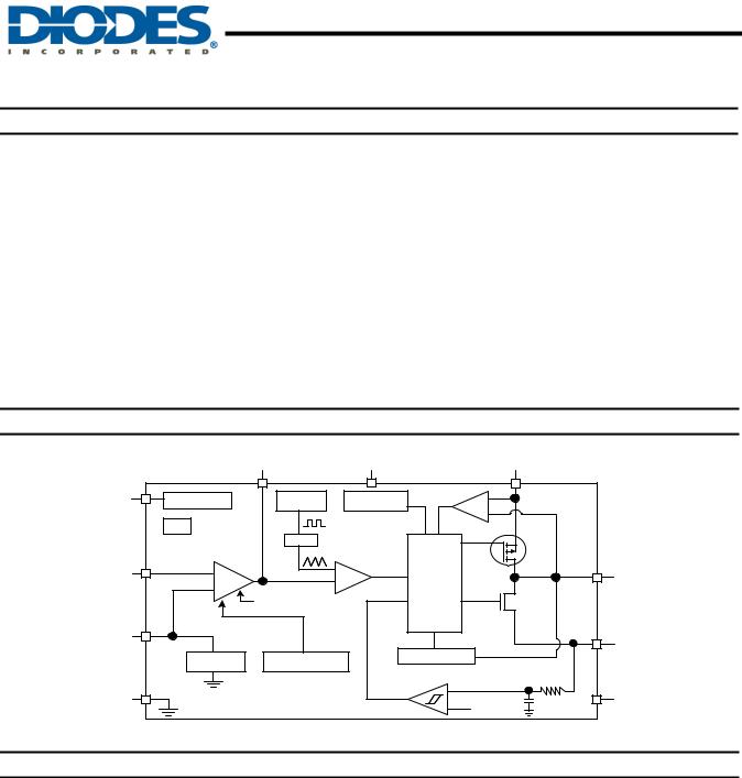
Functional Block Diagram
|
|
CC |
VCC |
|
OUT |
|
|
|
|
ZCR |
|
EN |
Schmitt-Trigger |
Oscillator |
Power - Good |
Comparator |
+ |
|
|||||
|
Bias |
|
|
|
- |
|
|
|
|
|
|
|
Error |
Ramp |
PWM |
|
|
|
|
PWM |
|
||
|
Amplifier |
|
Comparator |
|
|
FB |
- |
|
- |
Control |
LX |
|
& |
||||
|
+ |
|
+ |
||
|
Soft - Start |
|
Anti - |
|
|
|
|
|
Through |
|
|
|
|
|
|
Logic |
|
REF |
Vref=1.23V |
|
|
|
|
|
|
|
|
OCP |
|
|
|
|
|
Current - Limit |
|
|
BANDGAP |
Thermal - shutdown |
|
||
|
OCP |
|
|||
|
|
|
|
|
|
|
|
|
|
Comparator |
|
SGND |
|
|
|
+ |
PGND |
|
|
|
- |
||
|
|
|
|
0.16V |
|
Absolute Maximum Ratings
Symbol |
Parameter |
|
Rating |
|
Unit |
ESD HBM |
Human Body Model ESD Protection |
|
3 |
|
KV |
ESD MM |
Machine Model ESD Protection |
|
250 |
|
V |
|
OUT, VCC, EN, FB, OCP to GND |
|
-0.3 to +6.5 |
|
V |
|
LX to GND |
|
-0.3 to (OUT + 0.3) |
|
V |
ILX |
LX Current |
|
1.6 |
|
A |
|
REF, CC to GND |
|
-0.3 to (VCC + 0.3) |
|
V |
PD |
Continuous Power Dissipation (TA = 25oC) |
850 |
|
mW |
|
TJ |
Operating Junction Temperature Range |
-40 to +125 |
|
oC |
|
TST |
Storage Temperature Range |
|
-65 to +150 |
|
oC |
AP6714 |
|
2 of 11 |
|
|
April 2011 |
Document number: DS31490 Rev. 5 - 2 |
www.diodes.com |
|
© Diodes Incorporated |
||

AP6714
1.8MHz SYNCHRONOUS BOOST CONVERTER
Recommended Operating Conditions
Symbol |
Parameter |
Rating |
Unit |
|
|
TA |
Operating Ambient Temperature Range |
-40 to +85 |
oC |
|
VIN |
Supply Voltage at VIN (Note 3) |
0.9 to 5.5 |
V |
VOUT |
Output Voltage |
1.8 to 5.5 |
V |
|
Notes: |
3. The AP6714 is powered by step-up output. An internal low-voltage startup oscillator drives the starting at approximately 0.9V and the main |
|||
|
control will take over as soon as output is reached. AP6714 operation could be kept in low input voltage and output current is just limited. |
|||
Electrical Characteristics (VCC = 3V, TA = 25°C, unless otherwise specified)
Symbol |
Parameter |
Conditions |
Min |
Typ. |
Max |
Unit |
||
GENERAL |
|
|
|
|
|
|
||
ISTB |
|
Standby Current |
VCC = 3.6V ,VEN = 0V |
- |
0.5 |
1 |
µA |
|
ICC |
|
Supply Current |
VCC = EN = 3.6V, FB = 1.5V |
- |
150 |
300 |
µA |
|
REFERENCE |
|
|
|
|
|
|||
VREF |
|
Reference Output Voltage |
|
1.205 |
1.23 |
1.255 |
V |
|
VREF/ |
T |
Tempco of Reference |
-40 oC ≤ T ≤ 125 oC |
|
30 |
50 |
ppm/ oC |
|
VREF(LOAD) |
Reference Load Regulation |
10mA < ILOAD < 200mA |
- |
4.5 |
10 |
mV |
||
VREF(LINE) |
Reference Line Regulation |
2.8 < VCC < 5.5V |
- |
1.3 |
5 |
mV |
||
OSCILLATOR |
|
|
|
|
|
|||
FOSC |
|
OSC Frequency |
|
1400 |
1800 |
2200 |
KHz |
|
STEP-UP DC-TO-DC |
|
|
|
|
|
|||
VOUT/ |
T |
Tempco of Output Voltage |
IOUT = 10mA, -40 oC ≤ T≤ 85 oC |
|
50 |
100 |
ppm/ oC |
|
|
|
FB Input Leakage Current |
FB = 1.25V |
-100 |
0.01 |
+100 |
nA |
|
Duty |
|
Step-Up Maximum Duty Cycle |
FB = 0V |
80 |
85 |
90 |
% |
|
IOUT |
|
OUT Leakage Current |
VLX = 0V, OUT = 5V |
- |
1 |
5 |
µA |
|
ILXL |
|
LX Leakage Current |
VLX = OUT = 5V |
- |
2 |
5 |
µA |
|
RDS(ON) |
Switch On-Resistance |
N channel, Vcc = 5V |
- |
200 |
- |
mΩ |
||
P channel, Vcc = 5V |
- |
300 |
- |
|||||
|
|
|
|
|||||
ILM |
|
N-Channel Current Limit |
VIN = 1.5V (Note 4) |
1.2 |
1.4 |
1.6 |
A |
|
THERMAL-SHUTDOWN PROTECTION |
|
|
|
|
|
|||
|
|
Thermal Shutdown |
|
- |
150 |
- |
oC |
|
|
|
Thermal Hysteresis |
|
- |
40 |
- |
oC |
|
LOGIC INPUTS |
|
|
|
|
|
|||
|
|
EN Input Low Level |
1.5V < VCC < 5.5V |
- |
- |
0.4 |
V |
|
|
|
EN Input High Level |
1.5V < VCC < 5.5V |
0.8 |
- |
- |
V |
|
OVER CURRENT PROTECTION |
|
|
|
|
|
|||
VOCP |
|
Over Current Protection Voltage |
ROCP = 0.1Ω |
- |
0.16 |
- |
V |
|
THERMAL RESISTANCE |
|
|
|
|
|
|||
θJA |
|
Thermal Resistance Junction-to- |
MSOP-10L (Note 5) |
|
161 |
|
oC/W |
|
|
|
Ambient |
|
|
|
|
|
|
θJC |
|
Thermal Resistance |
MSOP-10L (Note 5) |
|
43 |
|
oC/W |
|
|
Junction-to-Case |
|
|
|||||
|
|
|
|
|
|
|
||
Notes: |
4. The step-up current limit in startup refers to the LX switch current limit, not the output current limit. |
|
|
|
||||
5.Test condition for MSOP-10L: Device mounted on 2oz copper, minimum recommended pad layout on top & bottom layer with thermal vias, double sided FR-4 PCB.
AP6714 |
3 of 11 |
April 2011 |
Document number: DS31490 Rev. 5 - 2 |
www.diodes.com |
© Diodes Incorporated |

|
|
|
|
|
|
|
|
|
|
|
|
|
|
|
AP6714 |
|
|
|
|
|
|
|
|
|
|
1.8MHz SYNCHRONOUS BOOST CONVERTER |
|||||||
Typical Operating Characteristics |
|
|
|
|
|
|
|
|
|
|
||||||
|
300 |
|
|
|
|
|
|
|
|
300 |
|
|
|
|
|
|
|
275 |
|
|
|
|
|
|
|
|
275 |
|
|
|
|
|
|
A) |
250 |
|
|
|
|
|
|
|
A) |
250 |
|
|
|
|
|
|
NT (μ |
225 |
|
|
|
|
|
|
|
NT (μ |
225 |
|
|
|
|
|
|
URRE |
|
|
|
|
|
|
|
URRE |
|
|
|
|
|
|
||
200 |
|
|
|
|
|
|
|
200 |
|
|
|
|
|
|
||
LY C |
175 |
|
|
|
|
|
|
|
LY C |
175 |
|
|
|
|
|
|
SUPP |
150 |
|
|
|
|
|
|
|
SUPP |
150 |
|
|
|
|
VIN |
= 2.4V |
|
|
|
|
|
|
|
|
|
|
|
|
|
|
|
||
|
|
|
|
|
|
|
|
|
|
|
|
|
|
|
V |
= 3.6V |
|
125 |
|
|
|
|
|
|
|
|
125 |
|
|
|
|
IN |
|
|
|
|
|
|
|
|
|
|
|
|
|
|
|
|
||
|
100 |
0.9 |
1.5 |
1.8 2.4 |
3 |
3.6 |
4.2 |
5 |
|
100 |
-40 |
-25 |
|
25 |
85 |
125 |
|
|
|
INPUT VOLTAGE (V) |
|
|
|
|
|
TEMPERATURE (°C) |
|
||||||
|
|
Fig. 1 Supply Current vs. Input Voltage |
|
|
|
Fig. 2 Supply Current vs. Temperature |
||||||||||
|
1.4 |
|
VIN |
= 1.5V |
|
|
|
|
|
2050 |
|
|
|
|
|
|
|
|
|
|
|
|
|
|
|
|
|
|
|
|
|
||
|
1.2 |
|
VIN = 3.0V |
|
|
|
|
|
2000 |
|
|
|
|
|
|
|
RRCYAUB-NDSTENT (μA) |
|
|
|
|
|
|
|
|
|
|
|
|
|
|
||
1 |
|
|
|
|
|
|
|
CYQRUENEF (KHz) |
1950 |
|
|
|
|
|
|
|
0.8 |
|
|
|
|
|
|
|
1900 |
|
|
|
|
|
|
||
|
|
|
|
|
|
|
|
|
|
|
|
|
|
|
||
|
0.6 |
|
|
|
|
|
|
|
|
1850 |
|
|
|
|
|
|
|
0.4 |
|
|
|
|
|
|
|
|
1800 |
|
|
|
|
|
|
|
0.2 |
|
|
|
|
|
|
|
|
1750 |
|
|
|
|
|
|
|
0 |
-40 |
25 |
105 |
|
125 |
|
|
1700 |
-40 |
-25 |
25 |
85 |
105 |
125 |
|
|
|
|
|
|
|
|||||||||||
|
|
|
TEMPERATURE (°C) |
|
|
|
|
|
TEMPERATURE (°C) |
|
||||||
|
|
Fig. 3 Stand-by Current vs. Temperature |
|
|
|
|
Fig. 4 Frequency vs. Temperature |
|||||||||
|
88 |
|
|
|
|
|
|
|
|
1.26 |
|
VIN = 1.8V |
|
|
|
|
|
|
|
|
|
|
|
|
|
|
|
|
|
|
|
|
|
|
87 |
|
|
|
|
|
|
|
|
1.25 |
|
VIN = 3.6V |
|
|
|
|
|
|
|
|
|
|
|
|
|
|
|
|
|
|
|
||
(%) |
86 |
|
|
|
|
|
|
|
|
1.24 |
|
|
|
|
|
|
|
|
|
|
|
|
|
|
(V) |
|
|
|
|
|
|
|
|
DUTY |
85 |
|
|
|
|
|
|
|
1.23 |
|
|
|
|
|
|
|
84 |
|
|
|
|
|
|
|
REF |
1.22 |
|
|
|
|
|
|
|
AX |
|
|
|
|
|
|
|
V |
|
|
|
|
|
|
||
|
|
|
|
|
|
|
|
|
|
|
|
|
|
|
||
M |
|
|
|
|
|
|
|
|
|
|
|
|
|
|
|
|
|
83 |
|
|
|
|
|
|
|
|
1.21 |
|
|
|
|
|
|
|
82 |
|
|
|
|
|
|
|
|
1.2 |
VOUT |
= 5.5V |
|
|
|
|
|
|
|
|
|
|
|
|
|
|
|
|
|
|
|
||
|
81 |
|
|
|
|
|
|
|
|
1.19 |
IOUT = 10mA |
|
|
|
|
|
|
-40 |
-25 |
25 |
85 |
105 |
125 |
|
-40 |
-25 |
|
25 |
105 |
125 |
|||
|
|
|
|
|
||||||||||||
|
|
|
TEMPERATURE (°C) |
|
|
|
|
|
TEMPERATURE (°C) |
|
||||||
|
|
|
|
|
|
|
|
Fig. 6 V vs. Temperature |
|
|||||||
|
|
|
Fig. 5 Max Duty vs. Temperature |
|
|
|
|
|
||||||||
|
|
|
|
|
|
|
|
REF |
|
|
|
|||||
AP6714 |
4 of 11 |
April 2011 |
Document number: DS31490 Rev. 5 - 2 |
www.diodes.com |
© Diodes Incorporated |
 Loading...