


A Product Line of
Diodes Incorporated
PAM2305D
1A STEP-DOWN DC-DC CONVERTER
Description |
|
Pin Assignments |
The PAM2305D is a step-down current-mode, DC-DC converter. At heavy load, the constant frequency PWM control per forms excellent stability and transient response. To ensure the longest battery life in portable applications, the PAM2305D provides a power-saving PulseSkipping Modulation (PSM) mode to reduce quiescent current under light load operation to save power.
The PAM2305D supports a range of input voltages from 2.5V to 5.5V, allowing the use of a single Li+/Li-polymer cell, multiple Alkaline/NiMH cell, USB, and other standard power sources. The output voltage is adjustable from 0.6V to the input voltage. All versions employ internal power switch and synchronous rectifier to minimize external part count and realize high efficiency. During shutdown, the input is disconnected from the output and the shutdown current is less than 0.1µA. Other key features include under-voltage lockout to prevent deep battery discharge.
The PAM2305D is available in TSOT25, DFN2x2-6 Pin and QFN3x316 Pin packages.
Features
•Efficiency up to 96%
•Only 40µA (typ) Quiescent Current
•Output Current: Up to 1A
•Internal Synchronous Rectifier
•1.5MHz Switching Frequency
•Soft Start
•Under-Voltage Lockout
•Short Circuit Protection
•Thermal Shutdown
•5-pin Small TSOT25, DFN2x2-6 Pin and QFN3x3-16 Pin Packages
•Pb-Free Packages
Top View
TSOT25
Applications
•Cellular Phone
•Portable Electronics
•Wireless Devices
•Cordless Phone
•Computer Peripherals
•Battery Powered Widgets
•Electronic Scales
•Digital Frame
PAM2305D |
1 of 15 |
January 2013 |
Document number: DSxxxxx Rev. 2 - 1 |
www.diodes.com |
© Diodes Incorporated |
A Product Line of
Diodes Incorporated
PAM2305D
Typical Applications Circuit
|
|
R1 |
|
|
VO = 0.6 × 1 |
+ |
|
|
|
R2 |
||||
|
|
|
Pin Descriptions
Pin |
|
Package Name |
Function |
||
Name |
TSOT25 |
DFN2x2-6L |
QFN3x3-16L |
||
|
|||||
VIN |
1 |
3 |
9, 10, 11, 12 |
Chip main power supply pin. |
|
GND |
2 |
5 |
1, 2, 3, 5 |
Ground. |
|
EN |
3 |
2 |
7 |
Enable Control Input. Force this pin voltage above 1.5V, enables the chip, and |
|
below 0.3V shuts down the device. |
|||||
|
|
|
|
||
FB |
4 |
6 |
4 |
Feedback voltage to internal error amplifier, the threshold voltage is 0.6V. |
|
SW |
5 |
4 |
13, 14, 15 |
The drains of the internal main and synchronous power MOSFET. |
|
NC |
— |
1 |
6, 8, 16 |
No connection. |
|
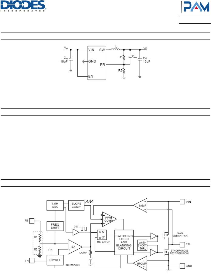
Functional Block Diagram
PAM2305D |
2 of 15 |
January 2013 |
Document number: DSxxxxx Rev. 2 - 1 |
www.diodes.com |
© Diodes Incorporated |

A Product Line of
Diodes Incorporated
PAM2305D
Absolute Maximum Ratings (@TA = +25°C, unless otherwise specified.)
These are stress ratings only and functional operation is not implied. Exposure to absolute maximum ratings for prolonged time periods may affect device reliability. All voltages are with respect to ground.
Parameter |
Rating |
Unit |
Input Voltage |
-0.3 to +6.0 |
V |
EN, FB Pin Voltage |
-0.3 to VIN |
V |
SW Pin Voltage |
-0.3 to (VIN +0.3) |
V |
Junction Temperature |
150 |
°C |
Storage Temperature Range |
-65 to +150 |
°C |
Soldering Temperature |
300, 5sec |
°C |
Recommended Operating Conditions (@TA = +25°C, unless otherwise specified.)
Parameter |
Rating |
Unit |
|
Supply Voltage |
2.5 to 5.5 |
V |
|
Operation Temperature Range |
-40 to +85 |
°C |
|
Junction Temperature Range |
-40 to +125 |
||
|
Thermal Information
|
Parameter |
Package |
Symbol |
Max |
Unit |
|
|
TSOT25 (Note 1) |
|
130 |
|
Thermal Resistance (Junction to Case) |
DFN2x2-6 |
θJC |
25 |
|
|
|
|
QFN3x3-16 |
|
14 |
°C/W |
|
|
TSOT25 |
|
250 |
|
|
|
|
|
||
Thermal Resistance (Junction to Ambient) |
DFN2x2-6 |
θJA |
68 |
|
|
|
|
QFN3x3-16 |
|
35 |
|
|
|
TSOT25 |
|
400 |
|
Internal Power Dissipation |
DFN2x2-6 |
PD |
980 |
mW |
|
|
|
QFN3x3-16 |
|
1470 |
|
Note: |
1. The maximun output current for TSOT25 package is limited by internal power dissipation capacity as described in |
||||
|
Application Information here inafter. |
|
|
|
|
PAM2305D |
3 of 15 |
January 2013 |
Document number: DSxxxxx Rev. 2 - 1 |
www.diodes.com |
© Diodes Incorporated |

A Product Line of
Diodes Incorporated
PAM2305D
Electrical Characteristics (@TA = +25°C, VIN = 3.6V, VO = 1.8V, CIN = 10µF, COUT = 10µF, L = 4.7µH, unless otherwise specified.)
Parameter |
Symbol |
Test Conditions |
Min |
Typ |
Max |
Units |
|
Input Voltage Range |
VIN |
|
|
2.5 |
|
5.5 |
V |
Regulated Feedback Voltage |
VFB |
|
|
0.588 |
0.6 |
0.612 |
V |
Reference Voltage Line Regulation |
VFB |
|
|
|
0.3 |
|
%/V |
Regulated Output Voltage Accuracy |
VO |
IO = 100mA |
|
-3 |
|
+3 |
% |
Peak Inductor Current |
IPK |
VIN = 3V,VFB = 0.5V or VO = 90% |
|
1.5 |
|
A |
|
Output Voltage Line Regulation |
LNR |
VIN = 2.5V to 5V, IO = 10mA |
|
0.2 |
0.5 |
%/V |
|
Output Voltage Load Regulation |
LDR |
IO = 1mA to 800mA |
|
|
1.5 |
|
% |
Quiescent Current |
IQ |
No load |
|
|
40 |
70 |
µA |
Shutdown Current |
ISD |
VEN = 0V |
|
|
0.1 |
1 |
µA |
Oscillator Frequency |
fOSC |
VO = 100% |
|
1.2 |
1.5 |
1.8 |
MHz |
VFB = 0V or VO = 0V |
|
|
500 |
|
kHz |
||
|
|
|
|
|
|||
Drain-Source On-State Resistance |
RDS(ON) |
IDS = 100mA |
P MOSFET |
|
0.3 |
0.45 |
Ω |
N MOSFET |
|
0.35 |
0.5 |
Ω |
|||
|
|
|
|
||||
SW Leakage Current |
ILSW |
|
|
|
±0.01 |
1 |
µA |
EN Threshold High |
VEH |
|
|
1.5 |
|
|
V |
EN Threshold Low |
VEL |
|
|
|
|
0.3 |
V |
EN Leakage Current |
IEN |
|
|
|
±0.01 |
|
µA |
Over Temperature Protection |
OTP |
|
|
|
150 |
|
°C |
OTP Hysteresis |
OTH |
|
|
|
30 |
|
°C |
PAM2305D |
4 of 15 |
January 2013 |
Document number: DSxxxxx Rev. 2 - 1 |
www.diodes.com |
© Diodes Incorporated |

A Product Line of
Diodes Incorporated
PAM2305D
Typical Performance Characteristics (@TA = +25°C, CIN = 10µF, CO = 10µF, L = 4.7µH, unless otherwise specified.)
PAM2305D |
5 of 15 |
January 2013 |
Document number: DSxxxxx Rev. 2 - 1 |
www.diodes.com |
© Diodes Incorporated |
 Loading...