


AVC-4320
Table of contents
 Loading...
For U.S.A. & Canada model
SERVICE MANUAL
Ver. 1
MODEL
AVR-4306
AVC-4320
AV SURROUND RECEIVER/AMPLIFIER
注 意
サービスをおこなう前に、このサービスマニュアルを
必ずお読みください。本機は、火災、感電、けがなど
に対する安全性を確保するために、さまざまな配慮を
おこなっており、また法的には「電気用品安全法」に
もとづき、所定の許可を得て製造されております。
従ってサービスをおこなう際は、これらの安全性が維
持されるよう、このサービスマニュアルに記載されて
いる注意事項を必ずお守りください。
●
For purposes of improvement, specifications and
design are subject to change without notice.
●
Please use this service manual with referring to the
operating instructions without fail.
●
Some illustrations using in this service manual are
slightly different from the actual set.
Denon Brand Company, D&M Holdings Inc.
●
●
●
●
TOKYO, JAPAN
本機の仕様は性能改良のため、予告なく変更すること
があります。
補修用性能部品の保有期間は、製造打切後8年です。
修理の際は、必ず取扱説明書を参照の上、作業を行っ
てください。
本文中に使用しているイラストは、説明の都合上現物
と多少異なる場合があります。
X0264-1 V.01 DE/CDM 0510
SAFETY PRECAUTIONS
The following check should be performed for the continued protection of the customer and service technician.
LEAKAGE CURRENT CHECK
Before returning the unit to the customer, make sure you make either (1) a leakage current check or (2) a line to chassis
resistance check. If the leakage current exceeds 0.5 milliamps, or if the resistance from chassis to either side of the power
cord is less than 460 kohms, the unit is defective.
AVR4306/AVC4320
CAUTION
Please heed the points listed below during servicing and inspection.
◎ Heed the cautions!
Spots requiring particular attention when servicing, such as
the cabinet, parts, chassis, etc., have cautions indicated on
labels or seals. Be sure to heed these cautions and the cautions indicated in the handling instructions.
◎ Caution concerning electric shock!
(1) An AC voltage is impressed on this set, so touching inter-
nal metal parts when the set is energized could cause
electric shock. Take care to avoid electric shock, by for example using an isolating transformer and gloves when
servicing while the set is energized, unplugging the power
cord when replacing parts, etc.
(2)There are high voltage parts inside. Handle with extra care
when the set is energized.
◎
Caution concerning disassembly and assembly!
Though great care is taken when manufacturing parts from
sheet metal, there may in some rare cases be burrs on the
edges of parts which could cause injury if fingers are moved
across them. Use gloves to protect your hands.
◎ Only use designated parts!
The set's parts have specific safety properties (fire resistance, voltage resistance, etc.). For replacement parts, be
sure to use parts which have the same properties. In particular, for the important safety parts that are marked ! on wiring
diagrams and parts lists, be sure to use the designated parts.
◎ Be sure to mount parts and arrange the
wires as they were originally!
For safety reasons, some parts use tape, tubes or other insulating materials, and some parts are mounted away from the
surface of printed circuit boards. Care is also taken with the
positions of the wires inside and clamps are used to keep
wires away from heating and high voltage parts, so be sure to
set everything back as it was originally.
◎ Inspect for safety after servicing!
Check that all screws, parts and wires removed or disconnected for servicing have been put back in their original positions, inspect that no parts around the area that has been
serviced have been negatively affected, conduct an insulation
check on the external metal connectors and between the
blades of the power plug, and otherwise check that safety is
ensured.
(Insulation check procedure)
Unplug the power cord from the power outlet, disconnect the
antenna, plugs, etc., and turn the power switch on. Using a
500V insulation resistance tester, check that the insulation resistance between the terminals of the power plug and the externally exposed metal parts (antenna terminal, headphones
terminal, microphone terminal, input terminal, etc.) is 1MΩ or
greater. If it is less, the set must be inspected and repaired.
CAUTION
Many of the electric and structural parts used in the set have
special safety properties. In most cases these properties are
difficult to distinguish by sight, and using replacement parts
with higher ratings (rated power and withstand voltage) does
not necessarily guarantee that safety performance will be preserved. Parts with safety properties are indicated as shown
below on the wiring diagrams and parts lists is this service
manual. Be sure to replace them with parts with the designated part number.
(1) Schematic diagrams ... Indicated by the ! mark.
(2) Parts lists ... Indicated by the ! mark.
Concerning important safety parts
Using parts other than the designated parts
could result in electric shock, fires or other
dangerous situations.
注 意
サービス、点検時にはつぎのことにご注意願います。
◎注意事項をお守りください!
サービスのとき特に注意を必要とする個所についてはキャ
ビネット、部品、シャーシなどにラベルや捺印で注意事項を
表示しています。これらの注意書きおよび取扱説明書などの
注意事項を必ずお守りください。
◎感電に注意!
(1) このセットは、交流電圧が印加されていますので通電時
に内部金属部に触れると感電することがあります。従っ
て通電サービス時には、絶縁トランスの使用や手袋の着
用、部品交換には、電源プラグを抜くなどして感電にご
注意ください。
(2) 内部には高電圧の部分がありますので、通電時の取扱に
は十分ご注意ください。
◎分解、組み立て作業時のご注意!
板金部品の端面の『バリ』は、部品製造時に充分管理をして
おりますが、板金端面は鋭利となっている箇所が有りますの
で、部品端面に触れたまま指を動かすとまれに怪我をする場
合がありますので十分注意して作業して下さい。手の保護の
ために手袋を着用してください。
◎指定部品の使用!
セットの部品は難燃性や耐電圧など安全上の特性を持った
ものとなっています。従って交換部品は、使用されていたも
のと同じ特性の部品を使用してください。特に配線図、部品
表に!印で指定されている安全上重要な部品は必ず指定の
ものをご使用ください。
◎部品の取付けや配線の引きまわしは、
元どおりに!
安全上、テープやチューブなどの絶縁材料を使用したり、プ
リント基板から浮かして取付けた部品があります。また内部
配線は引きまわしやクランパーによって発熱部品や高圧部
品に接近しないように配慮されていますので、これらは必ず
元どおりにしてください。
◎サービス後は安全点検を!
サービスのために取り外したねじ、部品、配線などが元どお
りになっているか、またサービスした個所の周辺を劣化させ
てしまったところがないかなどを点検し、外部金属端子部
と、電源プラグの刃の間の絶縁チェックをおこなうなど、安
全性が確保されていることを確認してください。
(絶縁チェックの方法)
電源コンセントから電源プラグを抜き、アンテナやプラグな
どを外し、電源スイッチを入れます。500V 絶縁抵抗計を用
いて、電源プラグのそれぞれの端子と外部露出金属部[アン
テナ端子、ヘッドホン端子マイク端子、入力端子など]との
間で、絶縁抵抗値が1 MΩ 以上であること、この値以下の
ときはセットの点検修理が必要です。
注 意
本機に使用している多くの電気部品、および機構部品は安全
上、特別な特性を持っています。この特性はほとんどの場合、
外観では判別つきにくく、またもとの部品より高い定格(定
格電力、耐圧)を持ったものを使用しても安全性が維持され
るとは、限りません。安全上の特性を持った部品は、この
サービスマニュアルの配線図、部品表につぎのように表示し
ていますので必ず指定されている部品番号のものを使用願
います。
(1) 配線図…
(2) 部品表…
安全上重要な部品について
!マークで表示しています。
!マークで表示しています。
指定された部品と異なるものを使用した場合に
は、感電、火災などの危険を生じる恐れがあり
ます。
2
DIMENSION
AVR-4306/AVC-4320
338.8
318.1
244.5
28.5
0
15
182.5
66.1
88.2
0
0
217
172
172
217
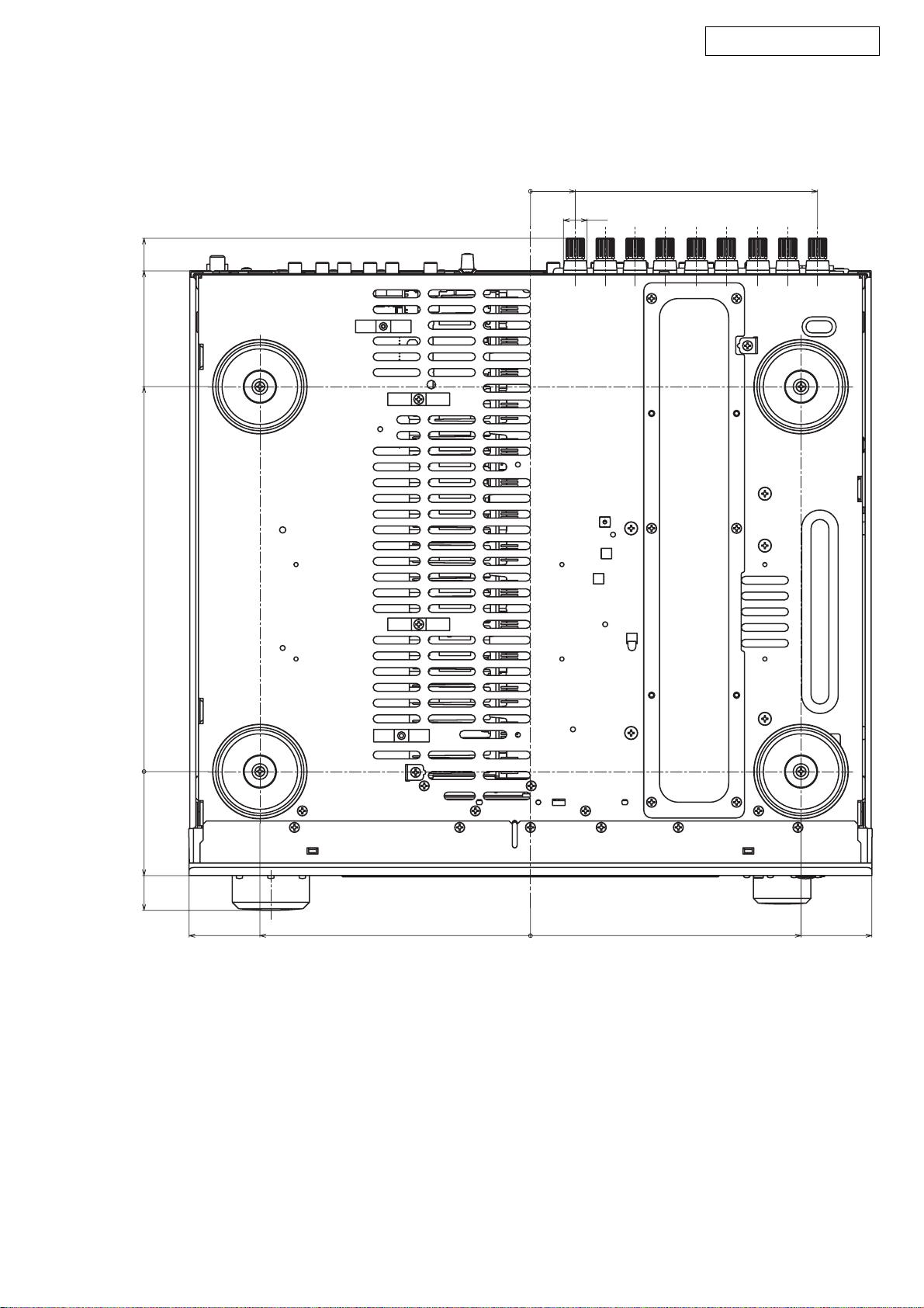
3
AVR-4306/AVC-4320
WIRE ARRANGEMENT
If wire bundles are untied or moved to perform adjustment or
parts replacement etc., be sure to rearrange them neatly as
they were originally bundled or placed afterward.
Otherwise, incorrect arrangement can be a cause of noise
generation.
Wire arrangement viewed from the top
Back Panel side
ワイヤー整形図
調整や部品の交換等により、ワイヤー類の結束をはずしたり移
動させた場合には、それらの作業が完了した時点でワイヤーの
整形をおこなってください。正しく整形されてないとノイズ発
生の原因となることがあります。
上面からみたワイヤー整形
Front Panel side
4
AVR-4306/AVC-4320
CAUTION IN SERVICING
Initializing AV SURROUND RECEIVER
AV SURROUND RECEIVER initialization should be performed
when the µcom, peripheral parts of µcom, and Digital P.W.B. are
replaced.
1. Switch off the unit.
2. Hold the following NIGHT button and PURE DIRECT button,
and switch on the unit.
3. Check that the entire display is flashing with an interval of
about 1 second, and release your fingers from the 2 buttons
and the microprocessor will be initialized.
Note:・If step 3 does not work, start over from step 1.
・ All user settings will be lost and this factory setting will
be recovered when this initialization mode.
So make sure to memorize your setting for restoring
after the initialization.
サービス時の注意事項
AVサラウンドアンプの初期化について
マイコンやマイコン周辺部品、Digital 基板等を交換した場合
は、AV サラウンドアンプの初期化を行って下さい。
1. オン/オフボタンを OFF にします。
2. NIGHT ボタンと PUREDIRECT ボタンを同時に押しながら、
オン/オフボタンを押して ON にします。
3. ディスプレイ表示が約 1秒間隔で点滅するのを確認後、2
つのボタンから指を離します。
*マイコンが初期化されます。
注意 : ・上記 3 の状態にならない場合は、もう一度操作 1 か
らやり直してください。
・初期化を行うとお客様が設定した内容が工場出荷状
態に戻りますので、あらかじめ設定内容を控えてお
き初期化後再設定してください。
5
AVR-4306/AVC-4320
ADJUSTMENT
Audio Section
Idling Current (1U-3701-1)
Required measurement equipment: DC Voltmeter
1. Preparation
(1) Avoid direct blow from an air conditioner or an electric
fan, and adjust the unit at normal room temperature 15 °C
~ 30 °C (59 °F ~ 86 °F).
(2) Presetting
• POWER (Power source switch) OFF
• SPEAKER (Speaker terminal) No load
(Do not connect speaker, dummy resistor, etc.)
2. Adjustment
(1) Remove top cover and set VR101, VR102, VR201,
VR301, VR302, VR401, VR402, on 1U-3701-1 (Power
Unit) at fully counterclockwise ( ).
(2) Connect DC Voltmeter to test points (FRONT-Lch:TP301
① ② pin, FRONT-Rch: TP101 ⑤ ⑥ pin, CENTER ch:
TP301③ ④pin, SURROUND-Lch: TP101③ ④pin, SURROUND-Rch: TP101 ① ② pin, SURROUND BACK-Lch:
TP301 ⑦ ⑧ pin, SURROUND BACK-Rch: TP301 ⑤ ⑥
pin).
(3) Connect power cord to AC Line, and turn power switch
"ON".
(4) Presetting.
MASTER VOLUME : "---" counterclockwise ( min.)
MODE : 7CH STEREO
FUNCTION : CD
(5) Allow 2 minutes, and turn VR101 clockwise ( ) to ad-
just the TEST POINT voltage to 6.5 mV ± 0.5 mV DC.
(6) After 10 minutes from preset, turn VR101 to set the volt-
age to 8 mV ± 0.5 mV DC.
(7) Adjust the Variable Resistors of other channels in the
same way.
(8) After 5 minutes from (6), turn VR101 to set the voltage to
8 m ± 0.5 mV DC.
(9) Adjust the Variable Resistors of other channels in the
same way.
調整
オーディオセクション
アイドリング電流の調整 (1U-3701-1)
調整に必要な測定器 : DCVoltmeter
1. 準備
(1) セットをクーラ、扇風機のそばなど風通しの良い場所
を避け、通常の使用状態に置きます。セットの周囲温
度は 15〜30 ℃、湿度は常湿とします。
(2) プリセット
・電源スイッチ OFF
・スピーカ端子 無負荷
( スピーカ・ダミー抵抗器などを接続しない。)
2. 調整
(1) 上カバーをはずし、1U-3701-1(パワーユニット)の
VR101,VR102,VR201,VR301,VR302,VR401,VR402 を反
時計方向 ( )に回し切った状態にセットします。
(2) テストポイント (FRONT-Lch:TP301 ①② pin,FRONT-
TP101 ⑤⑥ pin,CENTERch:TP301 ③④ pin,
Rch:
SURROUND-Lch:TP101 ③④ pin,SURROUND-Rch:
TP101 ①② pin,SURROUNDBACK-Lch:TP301 ⑦⑧ pin,
SURROUNDBACK-Rch:TP301 ⑤⑥ pin)に DC
Voltmeterを接続します。
(3) 電源コードを AC100V(95〜105Vの範囲でも可)に接
続し、電源スイッチを "ON"にします。
(4) ON後、次のようにセットします。
・MASTERVOLUME(音量調節つまみ)→反時計方向
( )に回す、最小の状態にする。
・SPEAKER(スピーカ端子)→無負荷(スピーカ、
ダミー抵抗器などを接続しない。)
MODE:7CHSTEREO
FUNCTION:CD
(5) 2分以内に VR101を時計方向 ( ) に回しテストポイ
ントの電圧を次のように調整します。
6.5mV ±0.5mVDC
(6) 予備調整から 10分後 VR101を回し、次のように電圧を
設定します。
8mV± 0.5mVDC
(7) 同じ方法で各チャネルの可変抵抗を調整します。
(8) (6) 項設定から 5分後 VR101を回し、次のように電圧を
設定します。
8mV± 0.5mVDC
(9) 同じ方法で各チャネルの可変抵抗を調整します。
6
DC Voltmeter
SR ch
VR302
8
7
6
5
4
3
2
1
SL ch
VR301
FR ch
VR102
FL ch
VR101
Cch
VR201
6
5
4
3
2
1
SBR ch
VR402
SR ch
SL ch
FR ch
FL ch
Cch
SBR ch
SBL ch
AVR-4306/AVC-4320
TP301
TP101
SBL ch
VR401
Audio Section
7

AVR-4306/AVC-4320
VIDEO Section
1. SETTING
(1) Connect the oscilloscope to the Y-signal and C-signal of
S MONITOR OUT terminal and each terminate at 75
Ohms.
(2) Connect the oscilloscope to the Y-signal, P
B-signal, PR-signal and CR-signal of COMPONENT
C
MONITOR OUT2 terminal and each terminate at 75
Ohms.
※ Use the 75 Ohms resistance must be 1%
(3) DVD test disc : DVDT-S01
(4) COMPONENT VIDEO OUT of DVD player is connected
to COMPONENT IN-1.
2. BEFORE ADJUSTMENT
2.1. Setting the Oscilloscope as below.
(1) PB/CB, PR/CR, C
(a) TIME/DIV : 10µs
(b) VOLT/DIV : 100mV
(Use the probe : x10 )
(2) Y
(a) TIME/DIV : 10µs
(b) VOLT/DIV : 200mV
(Use the probe : x10 )
Power on. Power Supply
USA, Canada & Taiwan R.O.C. : 120V
Europe & Asia : 230V
Japan : 100V
China & Korea : 220V
2.2. Setup the DVD player and confirmation of the
stators
(1) Set to "INTERLACED" mode at the COMPONENT OUT.
(2) Confirm the DVD player’s out put level is equal as the
item 2.4. in following.
2.3. Preparation
(1) Push [POWER] button with pressing [DSP SIMULA-
TION] and [STATUS] buttons.
(2) Confirm "0.0dB" appearing on the FL display.
(3) Turn the FUNCTION knob to select "DVD" input.
(4) Push [PURE DIRECT] button to select "PURE DIRECT".
(FL display disappears and becomes adjustment mode.)
(5) Push [OPEN/CLOSE] button of DVD player, then open
the Disc Tray.
Set DVD test disc (DVDT-S01) on the Disc Tray, and
then push [CLOSE] button.
(6) DVD player FL display appear "STOP", push [PLAY] but-
ton to playback DVD.
(7) Push the [DISPLAY] button of remote control of DVD
player unit and then appear the ON-Screen Display (GUI)
on the monitor TV.
(8) Push the [+10] and [2] button, select Title 12 of DVD.
(9) Push the [ENTER] button, playback Title 12.
(color bar 75%)
B-signal and
ビデオセクション
1. セッティング手順
(1) セットの SMONITOROUT端子から Y信号と C信号を
それぞれオシロスコープ(終端抵抗:75Ω)に接続し
ます。
(2) セットの COMPONENTMONITOROUT2の端子(Y,
B/CB,PR/CR)をそれぞれオシロスコープ(終端抵抗:
P
75Ω)に接続します。
※ 75Ω抵抗は 1%品を使用する事。
(3) DVDテストディスク:DVDT-S01を用意します。
(4) DVDプレーヤーの COMPONENTVIDEOOUTを
COMPONENTIN-1に接続します。
2. 調整のまえに
2.1. オシロスコープを下記に設定
(1) PB/CB,PR/CR,C
(a)TIME/DIV:10μs
(b)VOLT/DIV:100mV
(プローブ x10使用)
(2) Y
(a)TIME/DIV:10μs
(b)VOLT/DIV:200mV
(プローブ x10使用)
電源電圧:100V
2.2. DVDプレーヤの設定と確認
(1) COMPONENTOUTの設定を "インターレース "にしま
す。
(2) DVDプレーヤーの出力が以下 2.4.に合っていることを
確認します。
2.3. 準備手順
(1) セットの ACコードをコンセントへ挿入し、「DSP
SIMULATION」と「STATUS」ボタンを押しながらセッ
トの電源を"ON"にします。
(2) FL表示右上の VOL表示が "0.0dB"になっていることを
確認します。
(3) FUNCTIONノブを回し、入力を "DVD"に切り替えます。
(4) 「PUREDIRECT」ボタンを押し、"PUREDIRECT"にしま
す。(FL表示が消え、調整モードになります。)
(5) DVDプレーヤーの「OPEN/CLOSE」ボタンを押しトレ
イを開き、トレイ上に DVDテストディスク (DVDT-S01)
をセット後、「CLOSE」ボタンを押します。
(6) DVDプレーヤーの表示管上に "STOP"が表示されてか
ら、「PLAY」ボタンを押し、ディスクを再生します。
(7) DVDプレーヤーのリモコンの「DISPLAY」ボタンを押
しグラフィカル・ユーザー・インターフェイス (GUI)画
面を出します。
(8) 番号ボタンの「 +10」 ,「 2」ボタンを押し、Title12を選択
します。
(9) 「ENTER」ボタンを押し、Title12を再生します。
(75%カラーバー信号)
8
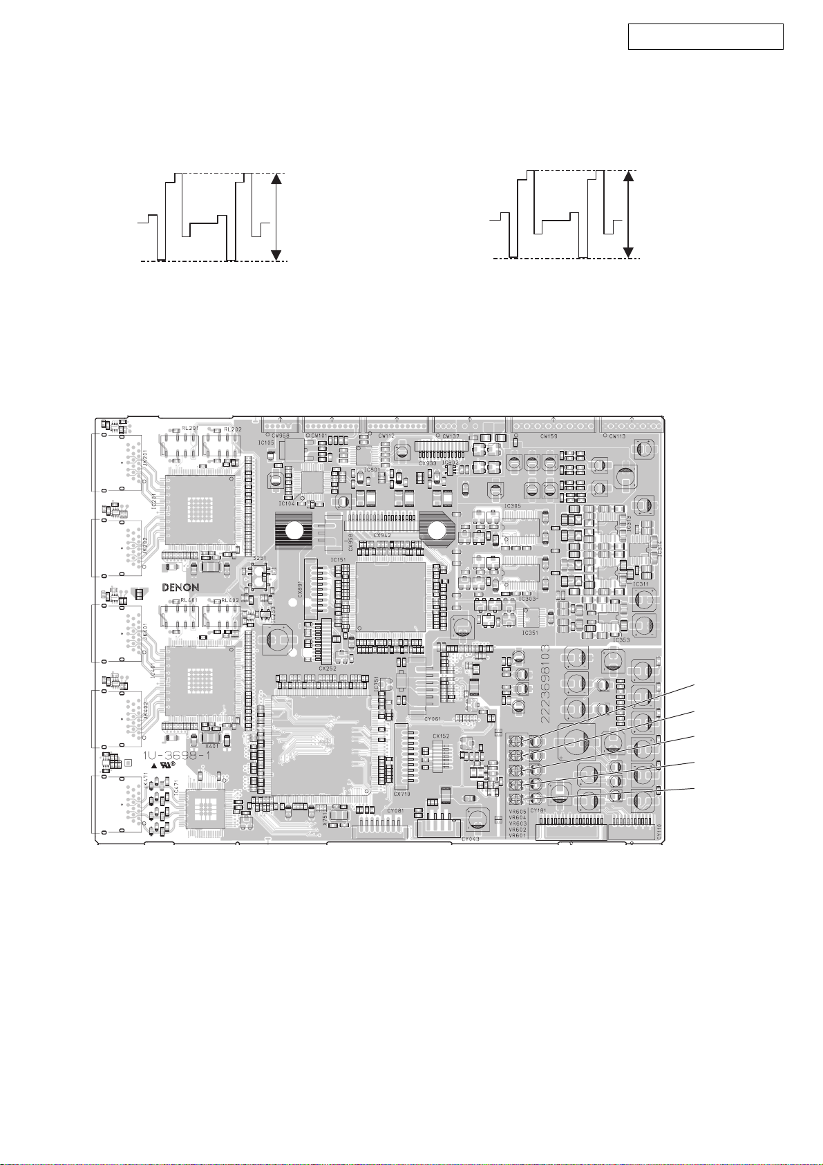
AVR-4306/AVC-4320
2.4. Procedure
(1) Adjust the signal of S MONITOR OUT by the wave of os-
cilloscope.
(a) Target, Y-signal
Point : 1U-3698 VR601
Adjustment Value : 714 ± 14mV
Waveform
Y
Y-signal of S MONITOR OUT
(b) Target, C-signal
Point : 1U-3698 VR602
Adjustment Value : 286 ± 5mV
Waveform
2.4. 手順
(1) セットの SMONITOROUT の信号レベルをオシロスコー
プ上の波高値で調整します。
(a) Y 信号レベル
調整個所 : 1U-3698VR601
調整値 : 714 ± 14mV
波形
Y
SMONITOROUT の Y 信号レベル
(b) C 信号レベル
調整個所 : 1U-3698VR602
調整値 : 286 ± 5mV
波形
C
C-signal of S-MONITOR OUT
(2) Adjust the signal of COMPONENT OUT by the wave of
oscilloscope.
(a) Target, Y-signal
Point : 1U-3698 VR603
Adjustment Value : 714 ± 14mV
Waveform
Y
Y-signal COMPONENT OUT
C
S-MONITOROUT の C 信号レベル
(2) COMPONENTOUTの信号レベルをオシロスコープ上の
波高値で調整します。
(a) Y 信号レベル
調整個所 : 1U-3698VR603
調整値 : 714 ± 14mV
波形
Y
COMPONENTOUT の Y 信号レベル
(b) Target, P
Point : 1U-3698 VR604
Adjustment Value : *525 ± 10mV
Waveform
B/CB-signal
PB/CB
PB/CB-signal COMPONENT OUT
B/CB 信号レベル
(b) P
調整個所 : 1U-3698VR604
調整値 : 525 ± 10mV
波形
PB/CB
COMPONENTOUT の PB/CB 信号レベル
9
AVR-4306/AVC-4320
(c) Target, P
Point : 1U-3698 VR605
Adjustment Value : *525 ± 10mV
Waveform
* : 486 ± 10mV for U.S.A. & Canada model
R/CR-signal
PR/CR-signal COMPONENT OUT
1U-3698 DIGITAL UNIT
PR/CR
(c) PR/CR 信号レベル
調整個所 : 1U-3698VR605
調整値 : 525 ± 10mV
波形
PR/CR
COMPONENTOUT の PR/CR 信号レベル
VR605 PR/CR
VR604 PB/CB
VR603 Y
VR602 S-C
VR601 S-Y
10
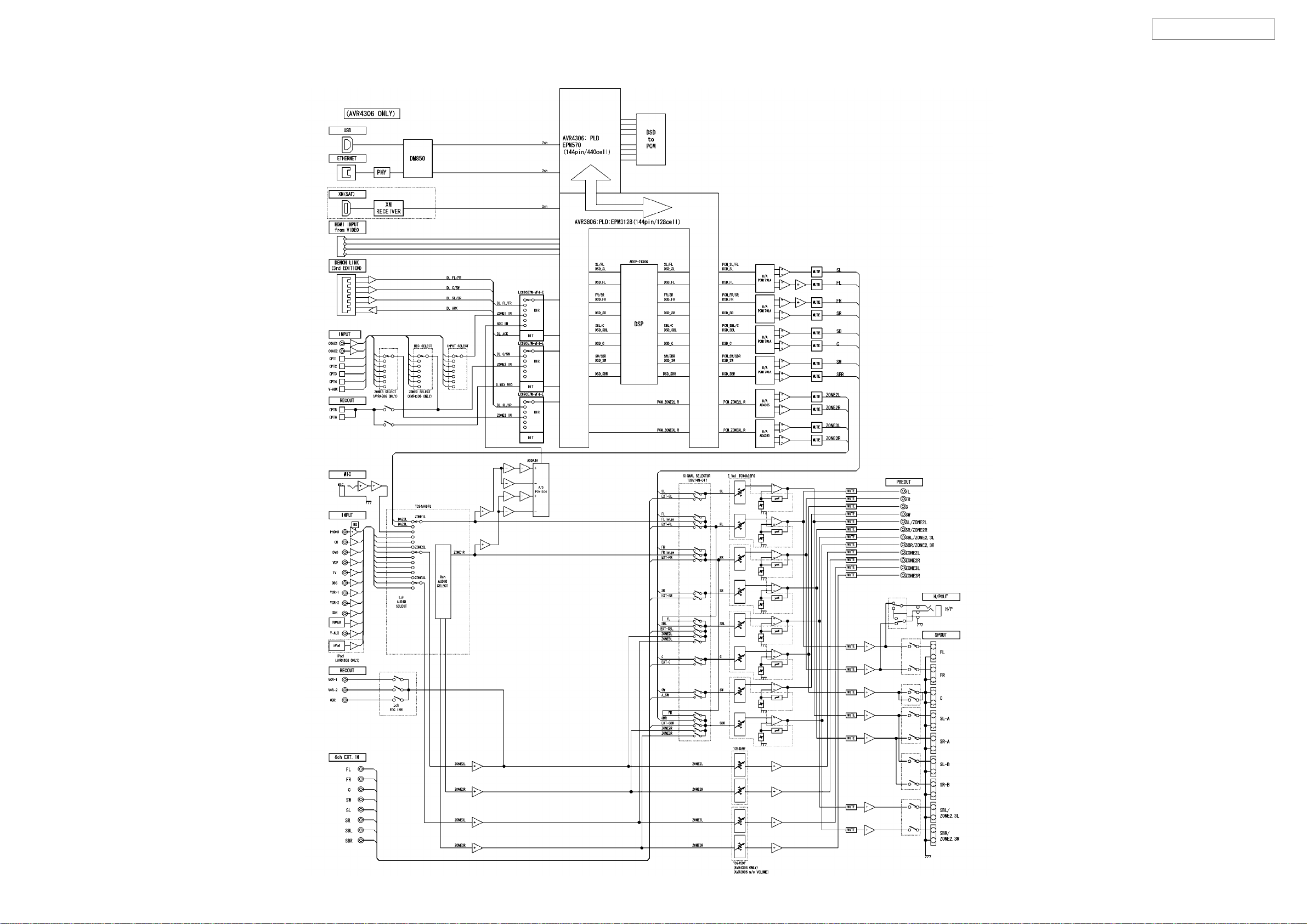
BLOCK DIAGRAMS (1/2)
AUDIO SECTION
AVR-4306/AVC-4320
11
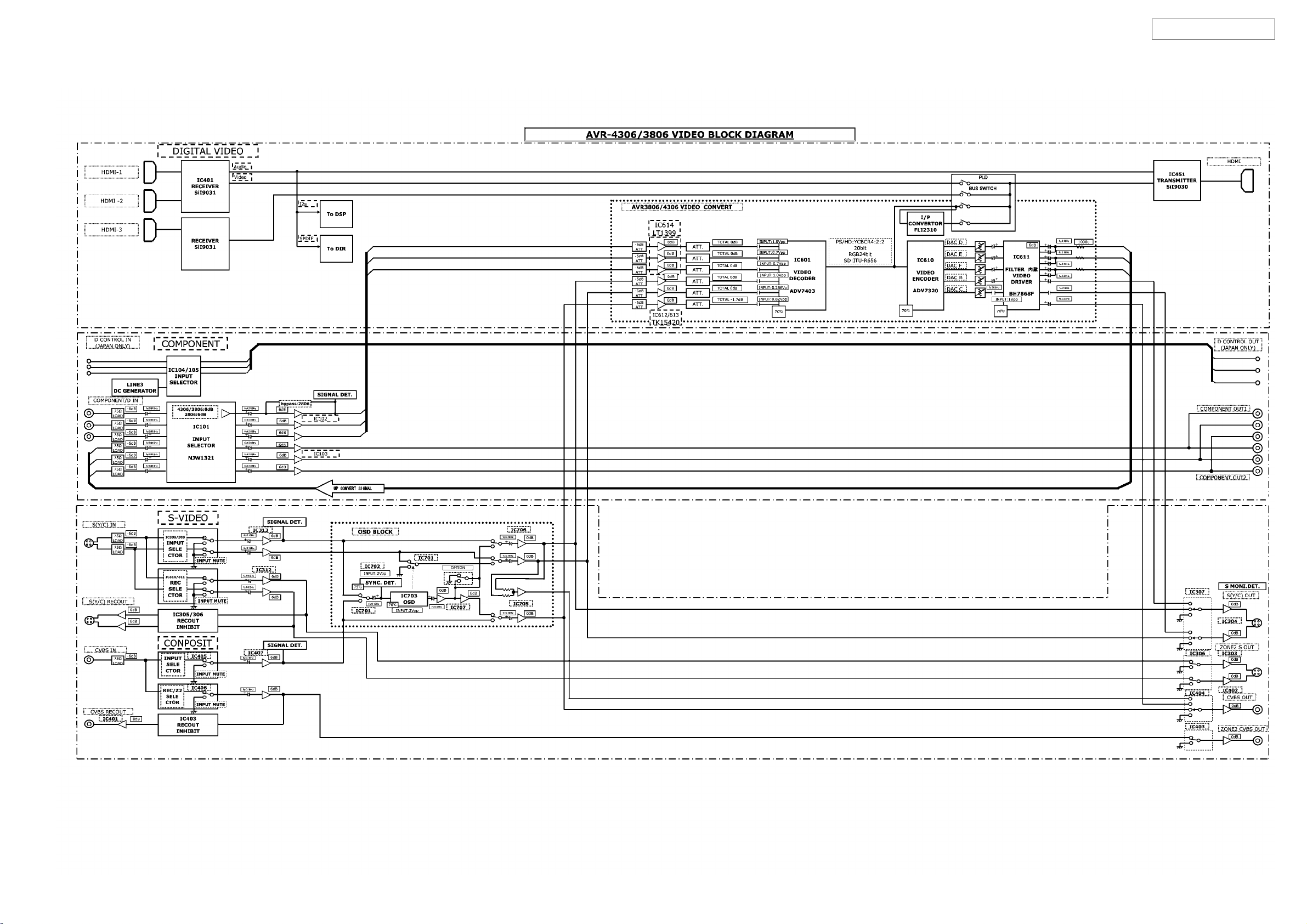
BLOCK DIAGRAMS (2/2)
VIDEO SECTION
AVR-4306/AVC-4320
12
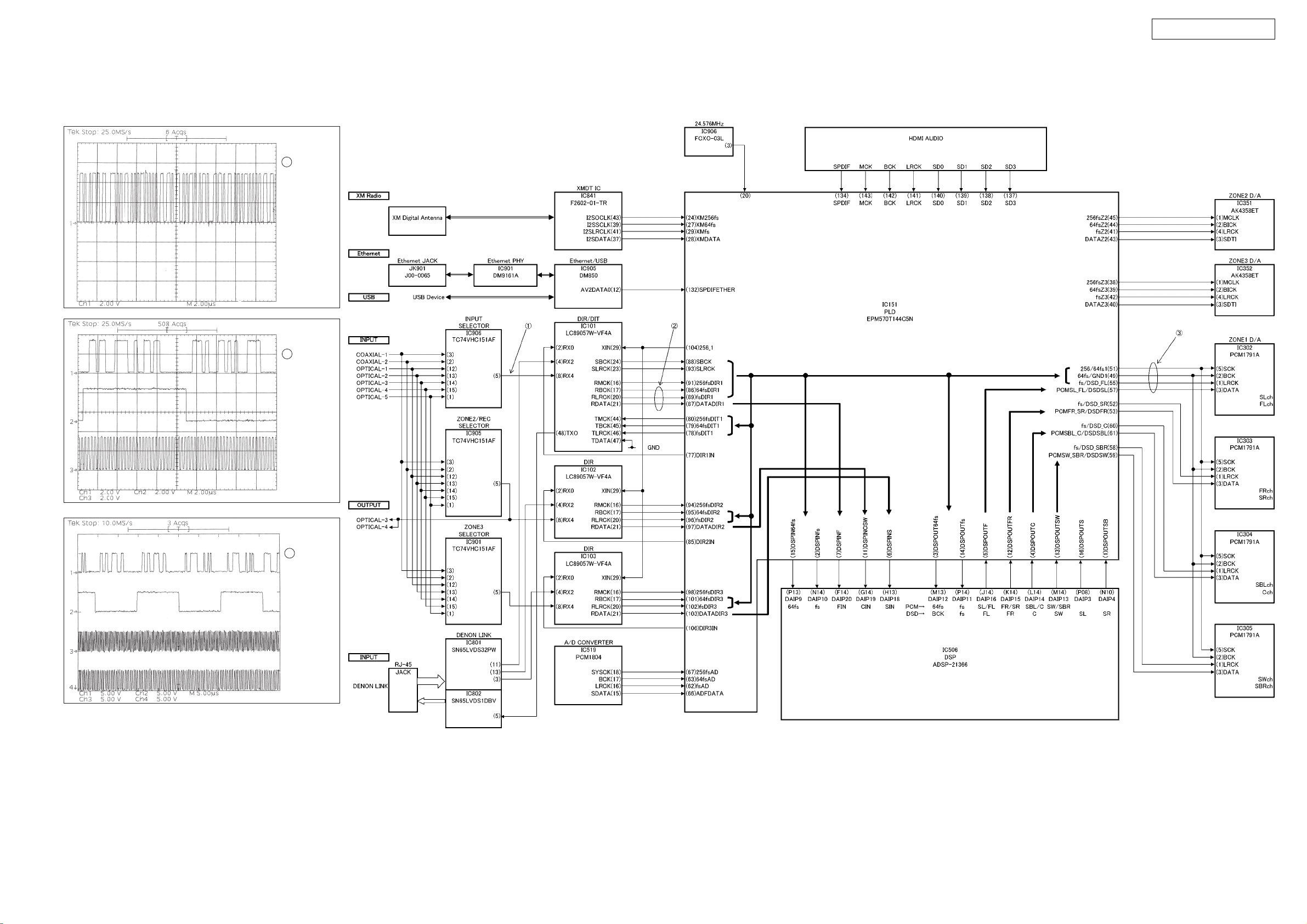
CLOCK FLOW & WAVE FORM IN DIGITAL BLOCK
Wave form
1
CH1: D-DATA
AVR-4306/AVC-4320
2
CH1: DATA
CH2: fs
CH3: 64fs
3
CH1: DATA
CH2: fs
CH3: 64fs
CH4: 256fs
13
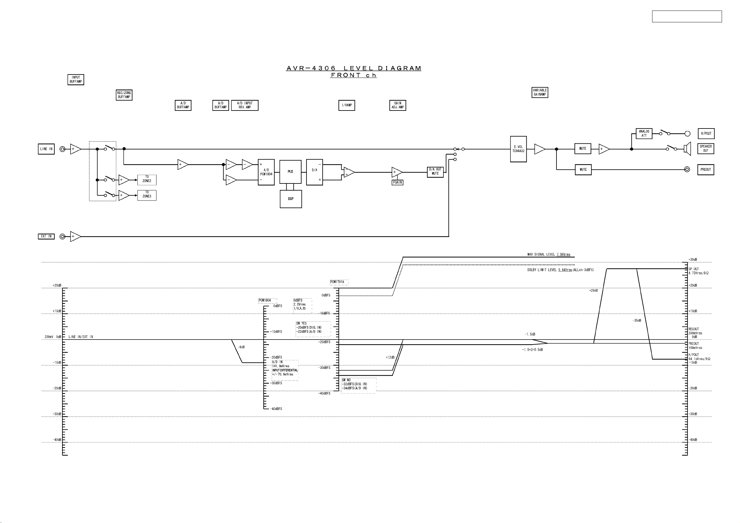
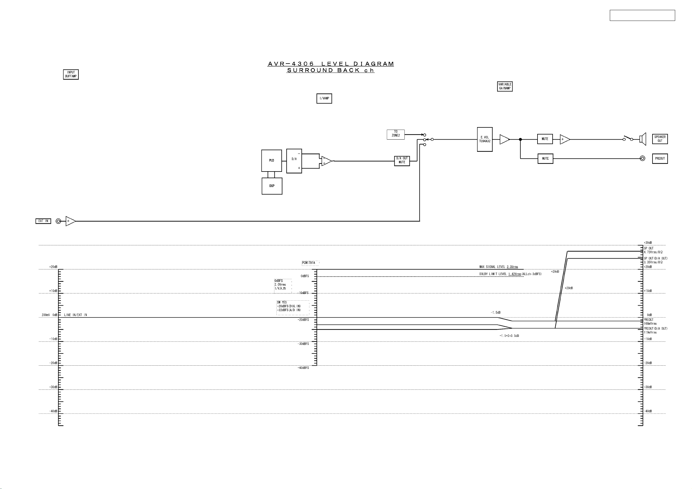
LEVEL DIAGRAMS (1/6)
AVR-4306/AVC-4320
14
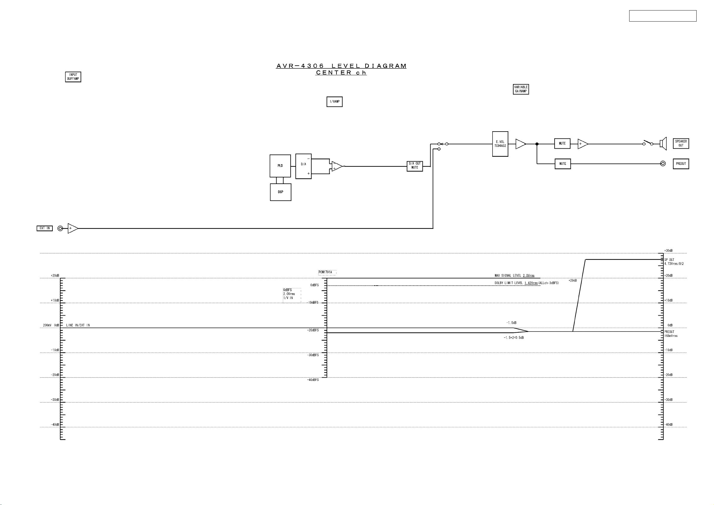
LEVEL DIAGRAMS (2/6)
AVR-4306/AVC-4320
15
LEVEL DIAGRAMS (3/6)
AVR-4306/AVC-4320
16
LEVEL DIAGRAMS (4/6)
AVR-4306/AVC-4320
17
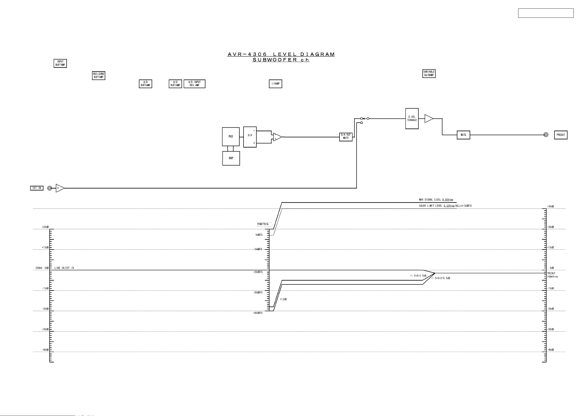
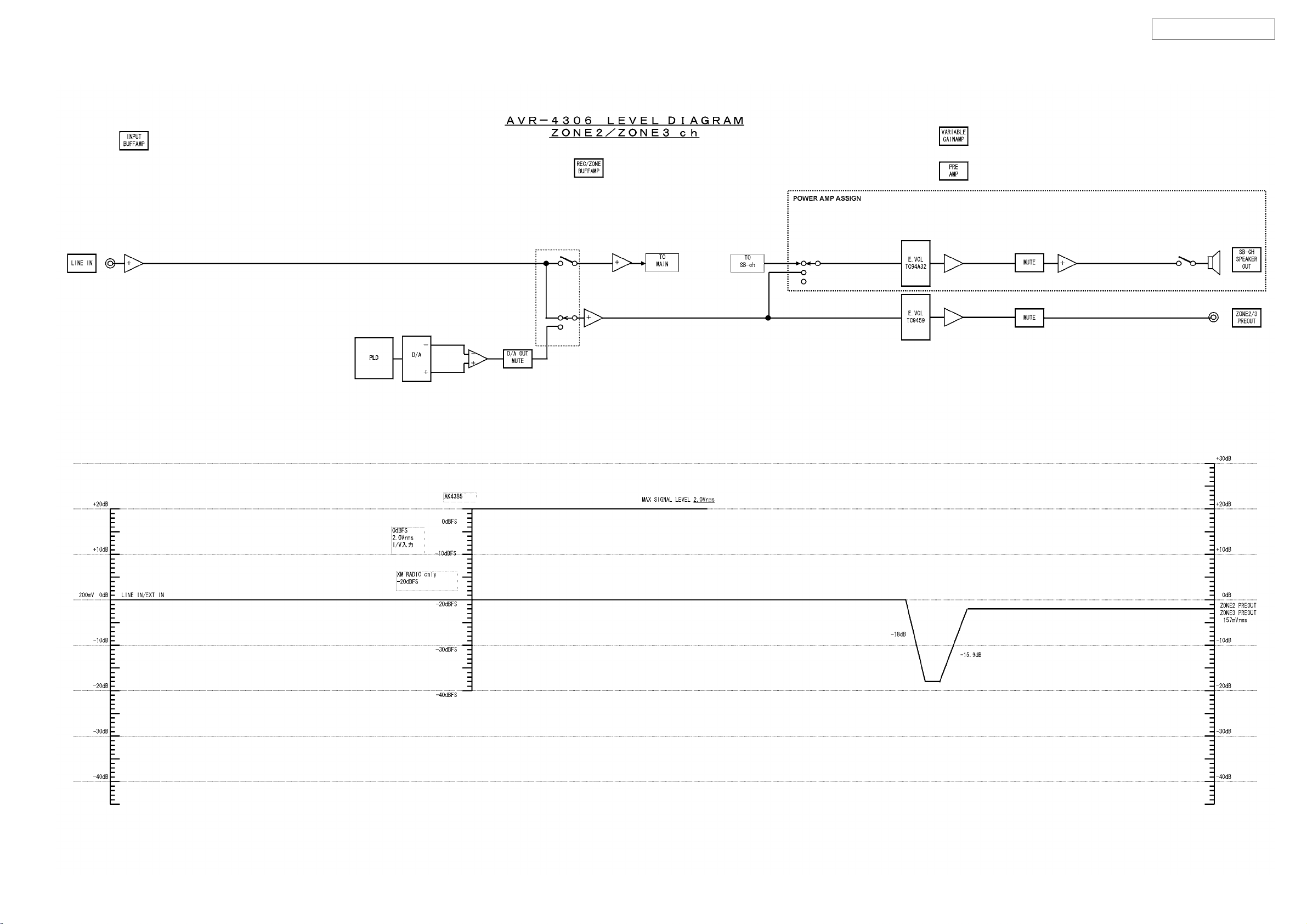
LEVEL DIAGRAMS (5/6)
AVR-4306/AVC-4320
18
LEVEL DIAGRAMS (6/6)
AVR-4306/AVC-4320
19
SEMICONDUCTORS
Only major semiconductors are shown, general semiconductors etc. are omitted to list.
主な半導体を記載しています。汎用の半導体は記載を省略しています。
1. IC’s
Note : Abbreviation ahead of IC No. indicates the name of P.W.B., etc.
注 ): ICNo. の前の記号は、基板の名称を表します。
MA : MAIN CPU P.W.B. FR : FRONT P.W.B.
PA : POWER AMP P.W.B. AV : AUDIO/VIDEO P.W.B.
PS : POWER SUPPLY P.W.B. DI : DIGITAL P.W.B.
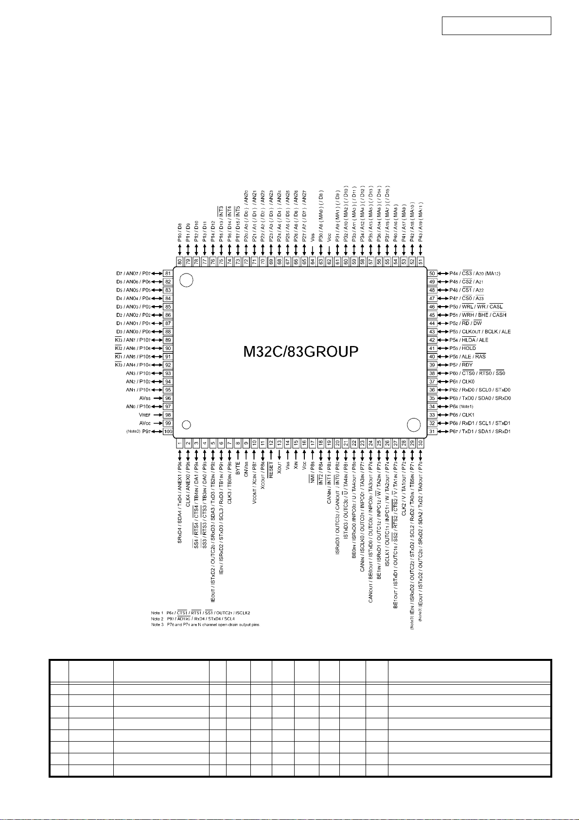
M30879FLFP (MA: IC506)
AVR-4306/AVC-4320
M30879FLFP Terminal Function
Pin
Pin Name Symbol I/O Type Det
No.
1 P96/SOUT4 E_SPIMOEI O C - - - Z O/L O/L ETHERNET comm. control pin
2 P95/CLK4 E_SPICLK O C - - - Z O/L O/L ETHERNET comm. control pin
3 P94/TB4 E_SPICS O C - - - Z O/L O/L ETHERNET comm. control pin
4 P93/TB3 ACKSIMO I - - - Ed Z O/L O/L MAIN-SUB µcom comm. control pin
5 P92/SOUT3 MOSI O C - - Ed Z O/L O/L MAIN-SUB µcom comm. control pin
6 P91/SIN3 SOMI O C - - Ed Z O/L O/L MAIN-SUB µcom comm. control pin
7 P90/CLK3 CLKMO O C - - Ed Z O/L O/L MAIN-SUB µcom comm. control pin
8 BYTE BYTE - - - - - - - - GND (Ext. data bus bit width switching, 16bit : L)
Op
(Int.)Op(Ext.)
Res STBY stop Function
20
AVR-4306/AVC-4320
Pin
Pin Name Symbol I/O Type Det
No.
9 CNVCS CNVSS I - - - Ed - - - Single-chip / Micro-processor mode switching
10 P87 RST SUB(RESET2) O C - - Ed Z O/L O/L SUB-µcom reset output
11 P86 E_RESET O C - - - Z O/L O/L ETHERNET comm. control pin
12 RESET RESET I - Lv - Eu L I I Reset input (Reset = "L")
13 XOUT X2 O - - - - - - - Clock output
14 VSS VSS - - - - - - - - GND
15 XIN X1 I - - - - - I I Clock input
16 VCC VCC - - - - - - - - +5V
17 P85/NMI _NMI I - - - - - - - Not used (Fixed to H)
18 P84/INT2 B.DOWN I -
19 P83/INT1 PROTECTION I -
20 P82/INT0 REMOCON I -
21 P81 EMODE I - Lv - Eu Z O/L O/L ETHERNET comm. control pin
22 P80/RXD5 RXD iPOD I - - - - Z O/L O/L IPOD comm. control pin
23 P77 REQ XM I - - - Ed Z O/L O/L XM RADIO control pin
24 P76/TXD5 TXD_iPOD O C - - - Z O/L O/L IPOD comm. control pin
25 P75 A.EXPOE O C - - Ed Z O/L O/L Audio expander control pin (TC4094BF)
26 P74 A.EXPSTB O C - - - Z O/L O/L Audio expander control pin (TC4094BF)
27 P73/CTS2 A.EXPD O C - - - Z O/L O/L
28 P72/CLK2 A.EXPCLK O C - - - Z O/L O/L Audio expander control CLK output pin (TC4094BF)
29 P71/RXD2 RXD MIXMO I - - - - Z I O/L XM RADIO control pin
30 P70/TXD2 TXD MOXMI O N - - Eu Z O/L O/L XM RADIO control pin
31 P67/TXD1 TXD MO232I O C - - Eu Z O/L O/L Data transfer output to outside (AMX)
32 P66/RXD1 RXD MI232O I - - - Ed Z I O/L Data receive input from outside (AMX)
33 P65/CLK1 VSCL I/O C - - Eu Z I O/L Video selector control pin (NJW1321)
34 P64/CTS1 VSDA I/O C - - Eu Z I O/L Video selector control pin (NJW1321)
35 P63/TXD0 E_TXDMOEI O C - - Z O/L O/L ETHERNET comm. control pin
36 P62/RXD0 E_RXDMIEO I - - - - Z O/L O/L ETHERNET comm. control pin
37 P61/CLK0 E.VOL_CLK O C - - - Z O/L O/L E-VR control output (TC94A32F, TC9459F)
38 P60/CTS0 E.VOL_DATA O C - - - Z O/L O/L E-VR control output (TC94A32F, TC9459F)
39 P57 E.VOL_STBA O C - - - Z O/L O/L E-VR control output (TC9459F)
40 P56 E.VOL_STBB O C - - - Z O/L O/L E-VR control output (TC94A32F)
41 P55/EPM FRASH EPM/MUTE POWER I/O - - - Eu Z I I Rewrite boot program start : L input set
42 P54 FUNC CLK O C - - - Z O/L O/L CLK output for function switching
43 P53 FUNC DATA O C - - - Z O/L O/L DATA output for function switching
44 P52 MIC DET I - Lv - Ed Z O/L O/L Microphone detect input
45 P51 STEREO I - Lv - Eu Z O/L O/L When TUNER FM stereo receive : L
46 P50/CE FRASH CE/TERST I/O - - - Ed Z I I Rewrite boot program start : H input set / Video for-
47 P47 TUNED I - Lv - Eu Z O/L O/L TUNER turned detect (Detected:L)
48 P46 TU STB O C - - - Z O/L O/L TUNER PLL control pin (LC72131)
49 P45 TU DOUT I - Lv - Ed Z I O/L TUNER PLL serial data input pin (LC72131)
50 P44 RDS DOUT I -
51 P43 TURDS CLK O C - - - Z O/L O/L PLL & RDS control pin (LC72131 & LC72720)
52 P42 TURDS DATA O C - - - Z O/L O/L PLL & RDS control pin (LC72131 & LC72720)
53 P41 RDS CE O C - - - Z O/L O/L RDS data output (LC72720)
54 P40 iPODDET I - Lv - - Z O/L O/L IPOD detect pin (Detected : L)
55 P37 VERST O C - - Ed Z O/L O/L Video encoder reset (ADV7320)
56 P36 VDRST O C - - Ed Z O/L O/L Video decoder reset (ADV7403BSTZ-110)
57 P35 OSD_STB O C - - - Z O/L O/L MAIN OSD control pin
58 P34 OSD_CLK O C - - - Z O/L O/L MAIN OSD control pin
59 P33 OSD_DATA O C - - - Z O/L O/L MAIN OSD control pin
60 P32 OSD_RST O C - - - Z O/L O/L MAIN OSD control pin
61 P31 SYNC.DET I - Lv - Eu Z I I Sync. detect input for MAIN (H : Ext. synchronized)
62 VCC VCC - - - - - - - - +5V
63 P30 COMP SDET I - Lv - Eu Z I O/L MAIN ZONE's COMPONENT signal detect input
64 VSS VSS - - - - - - - - GND
65 P27 Z1 VSIG.DET I - Lv - Eu Z I O/L
Op
(Int.)Op(Ext.)
- Eu Z I I Power down detect (Power down : L)
E
↓
L
- Ed Z I I Protection detect input (Detected : L)
E
↓
L
- - Z I I Remote control signal input
↑
L
E
- Eu Z I O/L RDS data input (LC72720)
E
↓
L
Res STBY stop Function
(Normal single-chip : L, Rewrite boot program start :
H input set)
Audio expander control DATA output pin (TC4094BF)
(TC9274N, TC94A46FG, TC9273N)
(TC9274N, TC94A46FG, TC9273N)
mat detector reset (TE8200PF)
MAIN ZONE's VIDEO signal detect input (Detected:H)
21
AVR-4306/AVC-4320
Pin
Pin Name Symbol I/O Type Det
No.
66 P26 Z1 SMONIDET I - - - Eu Z I O/L MAIN ZONE's S-monitor connection detect input
67 P25 Z1 SSIG.DET I - - - Eu Z I O/L MAIN ZONE's S-signal detect input (H : S-signal
68 P24 V.EXPCLK O C - - - Z O/L O/L CLK output for video expander control (TC4094BF)
69 P23 V.EXPD O C - - - Z O/L O/L
70 P22 V.EXPSTB O C - - - Z O/L O/L STB output for video expander control (TC4094BF)
71 P21 V.EXPOE O C - - Ed Z O/L O/L OE output for video expander control (TC4094BF)
72 P20 POSILOW I -
73 P17/INT5 EREQ I -
74 P16/INT4 REQSOMI I -
75 P15/INT3 POWER KEY I -
76 P14/D12 POWER O C - - Ed Z O/L O/L POWER relay control output (H : ON)
77 P13/D11 EPOWER O C - - Ed Z O/L O/L ETHERNET POWER control output (H : ON)
78 P12/D10 232C POWER O C - - Ed Z O/H O/L 232C POWER control pin (STANDBY : H)
79 P11/D9 REDLED O C - - Ed Z O/L O/L POWER/STANDBY LED control pin
80 P10/D8 GRNLED O C - - Ed Z O/L O/L POWER/STANDBY LED control pin
81 P07/D7 H/P DET I - - - Eu Z O/L O/L H/P detect input (Detected : H)
82 P06/D6 FL RST O C - - Ed Z O/L O/L FL DRIVER control pin
83 P05/D5 FL CE2 O C - - - Z O/L O/L FL DRIVER control pin
84 P04/D4 FL CE1 O C - - - Z O/L O/L FL DRIVER control pin
85 P03/D3 FL DATA O C - - - Z O/L O/L FL DRIVER control pin
86 P02/D2 FL CLK O C - - - Z O/L O/L FL DRIVER control pin
87 P01/D1 VSEL A I - Lv - Eu Z O/L O/L
88 P00/D0 VSEL B I - Lv - Eu Z O/L O/L
89 P107/AN7 ISEL A I - Lv - Eu Z O/L O/L Input selector rotation detect input (Rotary encoder)
90 P106/AN6 ISEL B I - Lv - Eu Z O/L O/L Input selector rotation detect input (Rotary encoder)
91 P105/AN5 KEY3 I - Lv - Eu Z O/L O/L Button input3
92 P104/AN4 KEY2 I - Lv - Eu Z O/L O/L Button input2
93 P103/AN3 KEY1 I - Lv - Eu Z O/L O/L Button input1
94 P102/AN2 ASIGDET I - Lv - - Z O/L O/L Signal detect input
95 P101/AN1 IPOD POWER O C - - - Z O/L O/L Power supply control pin for IPOD charge
96 AVS S AVS S - - - - - - - - A D GND
97 P100/AN0 MODE I - Lv - - Z O/L O/L Destination switching input
98 VREF VREF - - - - - - - - AD ref. +5V
99 AVC C AVC C - - - - - - - - AD + 5 V
100 P97/SIN4 E_SPIMIEO O C - - - Z O/L O/L ETHERNET comm. control pin
Op
(Int.)Op(Ext.)
- Ed Z O/L O/L Temperature detect (Detected : L)
E
↓
L
- - Z I O/L ETHERNET comm. control pin
E
↓
L
- - I O/L MAIN-SUB µcom comm. control pin
↓
L
E
- Eu Z I O/L Interrupt port for WAIT mode cancel
E
↓
L
Res STBY stop Function
(Connected:L )
inputted)
DATA output for video expander control (TC4094BF)
Mazter Volume rotation detect input (Rotary encoder)
Mazter Volume rotation detect input (Rotary encoder)
Note: Pin No. : Terminal number of microcomputer.
Port Name : The name entered in the data sheet of microcomputer.
Symbol : Symbolized interface function.
I/O : Input or out of part.
“I” = Input port
“O” = Output port
Type : Composition of port in case of output port.
“C” = CMOS output
“N” = NMOS open drain output
“P” = PMOS open drain output
Op : Pull up/Pull down selection information.
“Iu” = Inner microcomputer pull up
“Id” = Inner microcomputer pull down
“Eu” = External microcomputer pull up
“Ed” = External microcomputer pull down
Det : Indicates judging state of input port. Level detection is “LV”; Edge detection is “Ed”; Detection by both shifting is “E&L”;
Serial data detection is “S” (Serial data output is also “S”).
Res : State at reset.
“H” = Outputs High Level at reset
“L” = Outputs Low Level at reset
“Z” = Becomes High impedance mode at reset
STBY : State of port when STANDBY mode.
“O/L” = Output port and “L”
“I” = Input port
Stop : State of port when Stop mode.
“O/L” = Output port and “L”
“I” = Input port
22
M30624FGPGP (AD: IC517)
AVR-4306/AVC-4320
M30624FGPGP Terminal Function
Op
Pin
Pin Name Symbol I/O Type Det
No.
1 P94/TB4 DLINK ON O C - - - Z DENON LINK ON terminal (DENON LINK : H)
2 P93/TB3 DIRCE O C - - - Z DIR control pin (LC89057W)
3 P92/SOUT3 DIRDIN O C - - - Z DIR control pin (LC89057W)
4 P91/SIN3 DIRDOUT I - Lv - Eu Z DIR control pin (LC89057W)
5 P90/CLK3 DIRCLK O C - - - Z DIR control pin (LC89057W)
6 BYTE BYTE - - - - - - GND (Ext. data bus bit width switching, 16bit : L)
7 CNVCS CNVSS - - - - - - Single-chip / Micro-processor mode switching
8 P87 DSPBOOT I - - - Eu Z DSP rewrite boot program (DSP rewrite : L input)
9 P86 VSEL2 O C - - - Z Video PLD control pin (LC4064V-LC75TN100C)
10 RESET SUBRESET I - Lv - Eu L Reset input
11 XOUT X1 O - - - - - Oscillator connection
12 VSS VSS - - - - - - GND
13 XIN X2 I - - - - - Oscillator connection
14 VCC VCC - - - - - - +5V
15 P85/NMI _NMI I - - - - - Not used (Fixed to H)
16 P84/INT2 VSEL3 O C - - - Z Video PLD control pin (LC4064V-LC75TN100C)
17 P83/INT1 ACKSIMO I -
18 P82/INT0 SUBBDOWN I -
19 P81 VSEL4 O C - - - Z Video PLD control pin (LC4064V-LC75TN100C)
20 P80 VSEL0 O C - - - Z Video PLD control pin (LC4064V-LC75TN100C)
21 P77 VSEL1 O C - - - Z Video PLD control pin (LC4064V-LC75TN100C)
22 P76 PLD CS MAIN O C - - - Z Main PLD control pin (EPM3128ATC144-10)
23 P75 PLD DATA O C - - - Z Main PLD / Video PLD control pin
E
↓
L
↓
L
E
Op
(Int.)
- Ed Z MAIN/SUB-µcom control input (ACK from MAIN µcom L terurn)
Res FUNCTION
(Ext.)
(Normal single-chip : L, Rewrite boot program start : H input set)
Eu Z Power down detect (Power down : L)
(EPM3128ATC144-10, LC4064V-LC75TN100C)
23
AVR-4306/AVC-4320
Pin
Pin Name Symbol I/O Type Det
No.
24 P74 PLD CLK O C - - - Z Main PLD / Video PLD control pin
25 P73/CTS2 AD OVER L I - Lv - - Z LCH OVERLOAD
26 P72/CLK2 DIGITAL POWER O C - - Ed Z DIGITAL power on/off switching (ON : H)
27 P71/RXD2 SCL/EDIT SCL I/O C - - Eu Z VIDEO I2C/HDMI EDIT (E2PROM) control pin
28 P70/TXD2 SDA/EDIT SDA I/O C - - Eu Z VIDEO I2C/HDMI EDIT (E2PROM) control pin
29 P67/TXD1 TXD.S O C - - Eu Z Data transfer output to outside
30 P66/RXD1 RXD.S I - Lv - Eu Z Data receive input from outside
31 P65/CLK1 SCLK I - - - Eu Z for emulator
32 P64/CTS1 BUSY O C - - - Z for emulator
33 P63/TXD0 SOMI O C - - - Z MAIN-SUB µcom comm. control pin
34 P62/RXD0 SIMO I - - - Ed Z MAIN-SUB µcom comm. control pin
35 P61/CLK0 CLKSIMO I - - - Ed Z MAIN-SUB µcom comm. control pin
36 P60/CTS0 REQSOMI O C - - - Z MAIN-SUB µcom comm. control pin
37 P57 OSR2 O C - - Eu Z A/D control pin (PCM1804) 48kHz : L
38 P56 ADC RST O C - - Eu Z AD RST
39 P55/EPM (FRASH EPM)/(AUTH) I - Lv - - Z (Rewrite boot start : L) / (Test pin : AUTH)
40 P54 P1HPRMV2 O C - - - Z HP DET control pin for HDMI IN3 terminal
41 P53 P0HPRMV2 O C - - - Z HP DET control pin for HDMI IN2 terminal
42 P52 P1HPRMV1 O C - - - Z HP DET control pin for HDMI IN1 terminal
43 P51 (P0HPRMV1) O C - - - Z Not used
44 P50/CE FRASH CE/(AVMUTE) I - - - - Z Rewrite boot program start : H input set / (Test pin : AVMUTE)
45 P47 WP2 O C - - Ed Z HDMI IN1 EDIT (24LC02) WRITE PROTECT
46 P46 WP3 O C - - Ed Z HDMI IN1 EDIT (24LC02) WRITE PROTECT
47 P45 (WP0) O C - - Ed Z Not used
48 P44 WP1 O C - - Ed Z HDMI IN1 EDIT (24LC02) WRITE PROTECT
49 P43 INT2 I -
50 P42 INT1 I -
51 P41 SCDT2 I - - - - Z HDMI receiver (SiI9031) SCDT output (HDMI IN2/3)
52 P40 SCDT1 I - - - - Z HDMI receiver (SiI9031) SCDT output (HDMI IN1)
53 P37 HDMI R RST2 O C - - Ed Z HDMI receiver (SiI9031) reset (HDMI IN2/3)
54 P36 HDMI R RST1 O C - - Ed Z HDMI receiver (SiI9031) reset (HDMI IN1)
55 P35 HDMI T RST O C - - Ed Z HDMI TRANSMITTER reset (SiI9030)
56 P34 HDMI SENS I - Lv - - Z HDMI input signal detect input
57 P33 FGAIN O C - - Ed Z FGAIN control pin
58 P32 DACMDI/ZDACDATA O C - - - Z DAC control pin (PCM1791ADBR) / ZONE DAC controlpin (AK4385ET)
59 P31 DACMC/ZDACCLK O C - - - Z DAC control pin (PCM1791ADBR) / ZONE DAC controlpin (AK4385ET)
60 VCC VCC - - - - - - +5V
61 P30 DACMS O C - - - Z DAC control pin (PCM1791ADBR)
62 VSS VSS - - - - - - GND
63 P27 DACRST O C - - - Z DAC control pin (PCM1791ADBR)
64 P26 ZDACRST O C - - - Z ZONE DAC controlpin (AK4385ET)
65 P25 Z2DACCS O C - - - Z ZONE DAC controlpin (AK4385ET)
66 P24 Z3DACCS O C - - - Z ZONE DAC controlpin (AK4385ET)
67 P23 (SEL4FS) I/O C - - - Z Not used
68 P22 (SEL1FS) I/O C - - - Z Not used
69 P21 (INIT) I/O C - - - Z Not used
70 P20 DRECINH O C - - Ed Z Digital RECOUT INH control pin
71 P17/INT5 DRECC O C - - - Z Digital RECOUT switching
72 P16/INT4 DRECB O C - - - Z Digital RECOUT switching
73 P15/INT3 DRECA O C - - - Z Digital RECOUT switching
74 P14/D12 DINC O C - - - Z Digital input switching
75 P13/D11 DINB O C - - - Z Digital input switching
76 P12/D10 DINA O C - - - Z Digital input switching
77 P11/D9 VPP O C - - Eu - Normal : H, Writing flash ROM for DSP : L
78 P10/D8 DIR3 CKST O C - - Eu Z DIR control pin (LC89057W-VF4-E)
79 P07/D7 DIR2 CKST O C - - Eu Z DIR control pin (LC89057W-VF4-E)
80 P06/D6 DIR1 CKST O C - - Ed Z DIR control pin (LC89057W-VF4-E)
81 P05/D5 INT3 I -
82 P04/D4 INT2 I -
Op
Op
(Int.)
- - Z HDMI receiver (SiI9031) INT (HDMI IN2/3)
E
↓
L
- - Z HDMI receiver (SiI9031) INT (HDMI IN1)
E
↓
L
- Ed Z DIR control pin (LC89057W-VF4-E)
E
↓
L
- Eu Z DIR control pin (LC89057W-VF4-E)
E
↓
L
Res FUNCTION
(Ext.)
(EPM3128ATC144-10, LC4064V-LC75TN100C)
24
AVR-4306/AVC-4320
Pin
Pin Name Symbol I/O Type Det
No.
83 P03/D3 INT1 I -
84 P02/D2 DIRRST3 O C - - - Z DIR control pin (LC89057W-VF4-E)
85 P01/D1 DIRRST2 O C - - - Z DIR control pin (LC89057W-VF4-E)
86 P00/D0 DIRRST1 O C - - - Z DIR control pin (LC89057W-VF4-E)
87 P107/AN7 I/O POWER O C - - Eu Z POWER ON = "L" (After 10ms from DIGITAL POWER ON)
88 P106/AN6 DSPRST O C - - Ed Z DSP reset output pin (reset : L)
89 P105/AN5 DSPROMRST O C - - Ed Z Memory reset for DSP (reset : L)
90 P104/AN4 FLAG0 I - Lv - Ed Z DSP control pin (ADSP-21366)
91 P103/AN3 FLAG1 I - Lv - - Z DSP control pin (ADSP-21366)
92 P102/AN2 FLAG2 I - Lv - - Z DSP control pin (ADSP-21366)
93 P101/AN1 DSPICS O C - - - Z DSP control pin (ADSP-21366)
94 AVSS AVSS - - - - - - AD GND
95 P100/AN0 DSPOSCON O C - - - Z DSP OSC ON (DSP ON = "H" (After 20ms from DIGITAL POWER ON))
96 VREF VREF - - - - - - AD ref. +5V
97 AVC C AVCC - - - - - - AD + 5V
98 P97/SIN4 DSPOSI I - Lv - Eu Z DSP control pin (ADSP-21366)
99 P96/SOUT4 DSPISO O C - - - Z DSP control pin (ADSP-21366)
100 P95/CLK4 DSPICLK O C - - - Z DSP control pin (ADSP-21366)
Op
Op
(Int.)
- Ed Z DIR control pin (LC89057W-VF4-E)
E
↓
L
Res FUNCTION
(Ext.)
Note: Pin No. : Terminal number of microcomputer.
Port Name : The name entered in the data sheet of microcomputer.
Symbol : Symbolized interface function.
I/O : Input or out of part.
“I” = Input port
“O” = Output port
Type : Composition of port in case of output port.
“C” = CMOS output
“N” = NMOS open drain output
“P” = PMOS open drain output
Op : Pull up/Pull down selection information.
“Iu” = Inner microcomputer pull up
“Id” = Inner microcomputer pull down
“Eu” = External microcomputer pull up
“Ed” = External microcomputer pull down
Det : Indicates judging state of input port. Level detection is “LV”; Edge detection is “Ed”; Detection by both shifting is “E&L”;
Serial data detection is “S” (Serial data output is also “S”).
Res : State at reset.
“H” = Outputs High Level at reset
“L” = Outputs Low Level at reset
“Z” = Becomes High impedance mode at reset
STBY : State of port when STANDBY mode.
“O/L” = Output port and “L”
“I” = Input port
Stop : State of port when Stop mode.
“O/L” = Output port and “L”
“I” = Input port
25
TC4094BF(TP1) (MA: IC501, 502, 504, 508)
V
STROBE 1
V
Q1
Q2
Q3
Q4
SS
2
3
4
5
6
7
8
DATA
CLOCK
TC4094BF(TP1) Terminal Function
bit Port Symbol Function
EXP1 TRIGGER 2 TRIGGER OUT 2 control pin
EXP2 TRIGGER 1 TRIGGER OUT 1 control pin
EXP3 AD MUTE AD mute control pin
IC504
IC508
IC501
IC502
EXP4 PRE Z3 MUTE PREOUT mute control pin
EXP5 PRE Z2 MUTE PREOUT mute control pin
EXP6 PRE SB MUTE PREOUT mute control pin
EXP7 PRE S MUTE PREOUT mute control pin
EXP8 PRE SW MUTE PREOUT mute control pin
EXP9 PRE C MUTE PREOUT mute control pin
EXP10 PRE F MUTE PREOUT mute control pin
EXP11 LIMIT LIMIT control pin (7ch ST=H, EXT. IN = H)
EXP12 A+B LIMIT A+B LIMIT control pin (SURROUND SPEAKER A+B = H)
EXP13 RDS RST RDS reset (LC72720)
EXP14 T. MUTE Tuner mute control pin (MUTE = L)
EXP15 EQ GRN MULT EQ LED (GRN) control pin
EXP16 EQ RED MULT EQ LED (RED) control pin
EXP17 XM RST XM RADIO control pin
EXP18 XM COMMAND XM RADIO control pin
EXP19 SCPU POWER SUB CPU power on/off switching (H : ON)
EXP20 UART RL UART control switching pin (IPOD control = H)
EXP21 iPOD id IPOD control pin (iPod detect, iPod function switching = H)
EXP22 FSTB2 STB output for function switching control (TC94A46FG)
EXP23 FSTB1 STB output for RECINH/EXT. IN switching control (TC9273N-015, TC9274N-017)
EXP24 XM POWER XM RADIO power on/off switching (H : ON)
EXP25 BINRL AMP+B control
EXP26 F/S RL FRONT speaker relay control pin
EXP27 C RL CENTER speaker relay control pin
EXP28 SRA/FA RL SURROUND A speaker relay control pin
EXP29 SRB/FB RL SURROUND B speaker relay control pin
EXP30 SB RL SURROUND BACK speaker relay control pin
EXP31 HP RL H/P RELAY control pin
EXP32 VIDEO POWER Video power on/off switching (H : ON)
16
15
14
13
12
11
10
DD
OE
Q5
Q6
Q7
Q8
Q’
S
9
Q
S
AVR-4306/AVC-4320
26
BU4094BCFV-E2 (AV: IC708, 709, 710)
V
STROBE 1
V
Q1
Q2
Q3
Q4
SS
2
3
4
5
6
7
8
DATA
CLOCK
BU4094BCFV-E2 Terminal Function
bit Port Symbol Function
EXP1 IN A Video input select
EXP2 IN B Video input select
EXP3 IN C Video input select
IC708
IC709
IC710
IC711
EXP4 Z1IN INH Video input select
EXP5 REC A Video RECOUT select
EXP6 REC B Video RECOUT select
EXP7 REC C Video RECOUT select
EXP8 REC INH Video RECOUT select
EXP9 VCR1 INH Video RECOUT select (VCR1 INH)
EXP10 VCR2 INH Video RECOUT select (VCR2 INH)
EXP11 Z2 INH ZONE2 video output select (Z2 INH)
EXP12 Z1 VMONIA COMPOSIT MONITOR OUT video select
EXP13 Z1 VMONIB COMPOSIT MONITOR OUT video select
EXP14 Z1 SMONIA S MONITOR OUT video select
EXP15 Z1 SMONIB S MONITOR OUT video select
EXP16 S2_OUT S/COMPOSIT select control pin
EXP17 S1_IN S/COMPOSIT select control pin
EXP18 Z1 VOSD MAIN S OSD/OSD PASS select control pin
EXP19 Z1 SOSD MAIN S OSD/OSD PASS select control pin
EXP20 (Y/C SEL) Not used
EXP21 P.SAVE
EXP22 MONI DIS COMPONENT MONITOR disable control pin
EXP23 NC NC
EXP24 NC NC
EXP25 LINE A D connector LINE control pin
EXP26 LINE B D connector LINE control pin
EXP27 INH LINE D connector LINE control pin
EXP28 ASPECT H ASPECT ratio level control pin
EXP29 ASPECT L ASPECT ratio level control pin
EXP30 NC NC
EXP31 NC NC
EXP32 NC NC
16
DD
OE
15
14
Q5
13
Q6
12
Q7
11
Q8
10
Q’
S
9
Q
S
COMPONENT → CONVERT disable control pin
AVR-4306/AVC-4320
27
ADSP-21366SKBCZ (DI: IC506)
PIN A 1 INDICATOR
TOP VIEW
AVR-4306/AVC-4320
A
B
C
D
E
F
G
H
J
K
L
M
N
P
109876543211314 1112
BOTTOM VI EW
28
BR24L02F-WE2 (DI: IC204, 403, 404)
AVR-4306/AVC-4320
TC74HC151AF (MA: IC901, 905, 906)
29
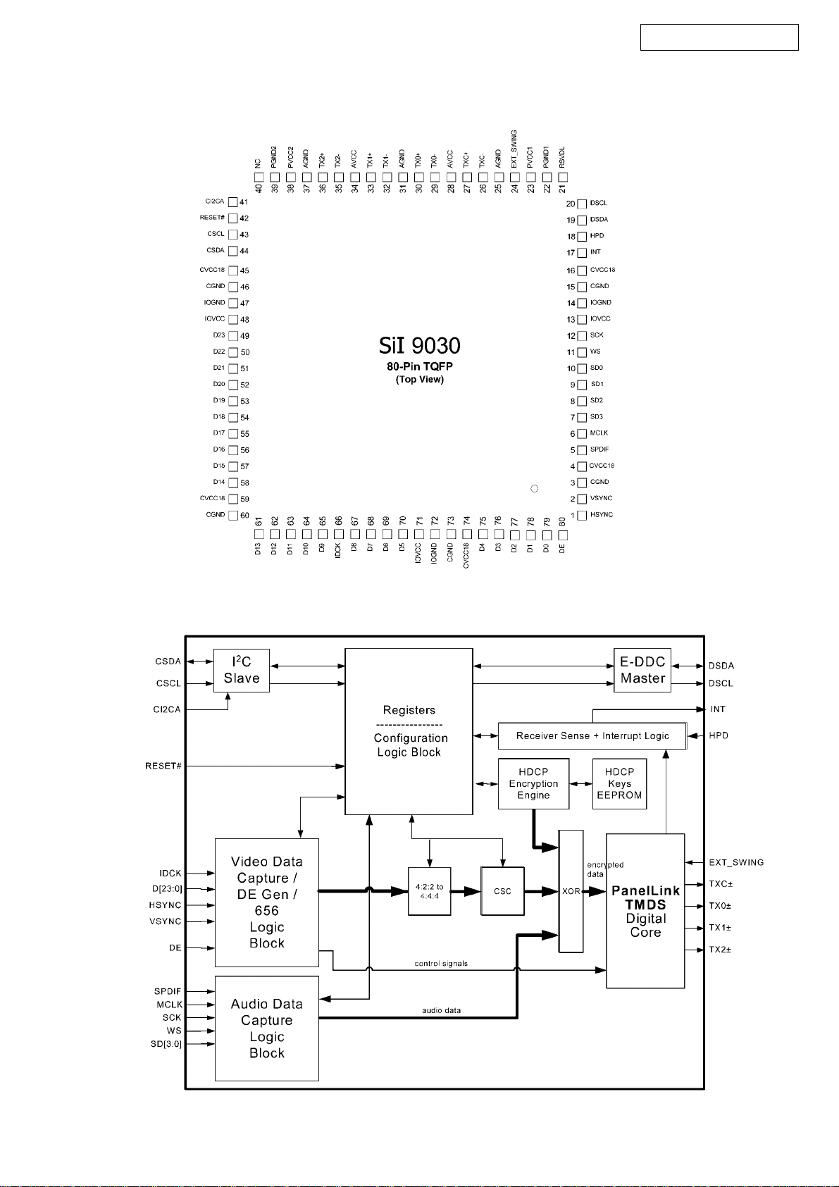
SiI9030CUT-7 (DI: IC471)
AVR-4306/AVC-4320
Functional Block Diagram
30
Loading...