


AVC-3570
Table of contents
 Loading...
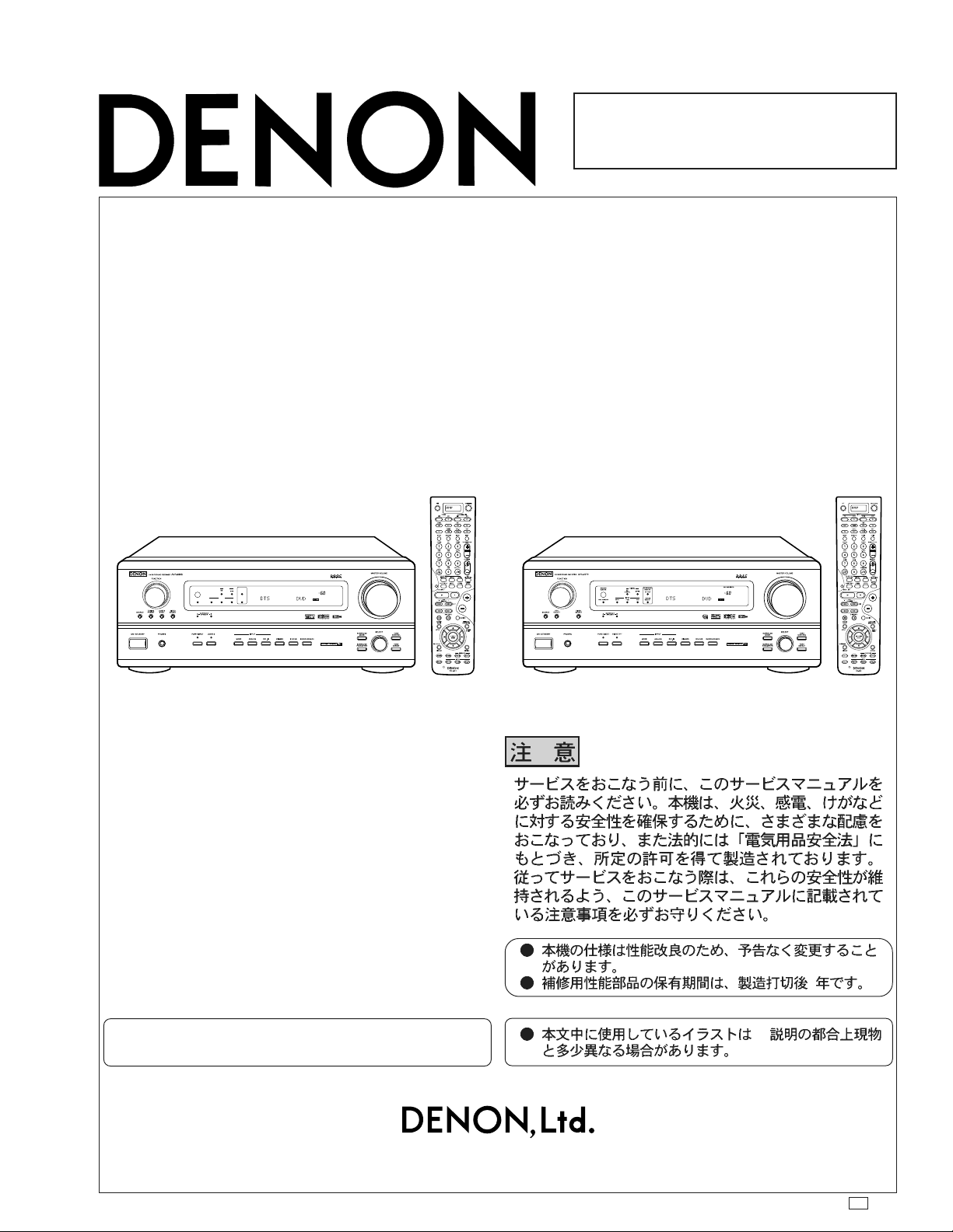
For U.S.A., Canada, Europe, Asia,
China, Hong Kong, Taiwan R.O.C.,
Korea & Japan model
SERVICE MANUAL
MODEL
AV SURROUND RECEIVER/AMPLIFIER
REMOTE
SURROUND
SIGNAL
SENSOR
BACK CH
OUTPUT
DIGITAL
INPUT
SIGNAL
ON / STANDBY
AUTO
DTS
PCM
DETECT
AVR-3803 AVC-3570
VOLUME LEVEL
AVR-3803/1083
AVC-3570
Some illustrations using in this service manual are
slightly different from the actual set.
16-11, YUSHIMA 3-CHOME, BUNKYOU-KU, TOKYO 113-0034 JAPAN
Telephone: 03 (3837) 5321
8
,
X0155 NC 0211
AVR-3803/1083/AVC-3570
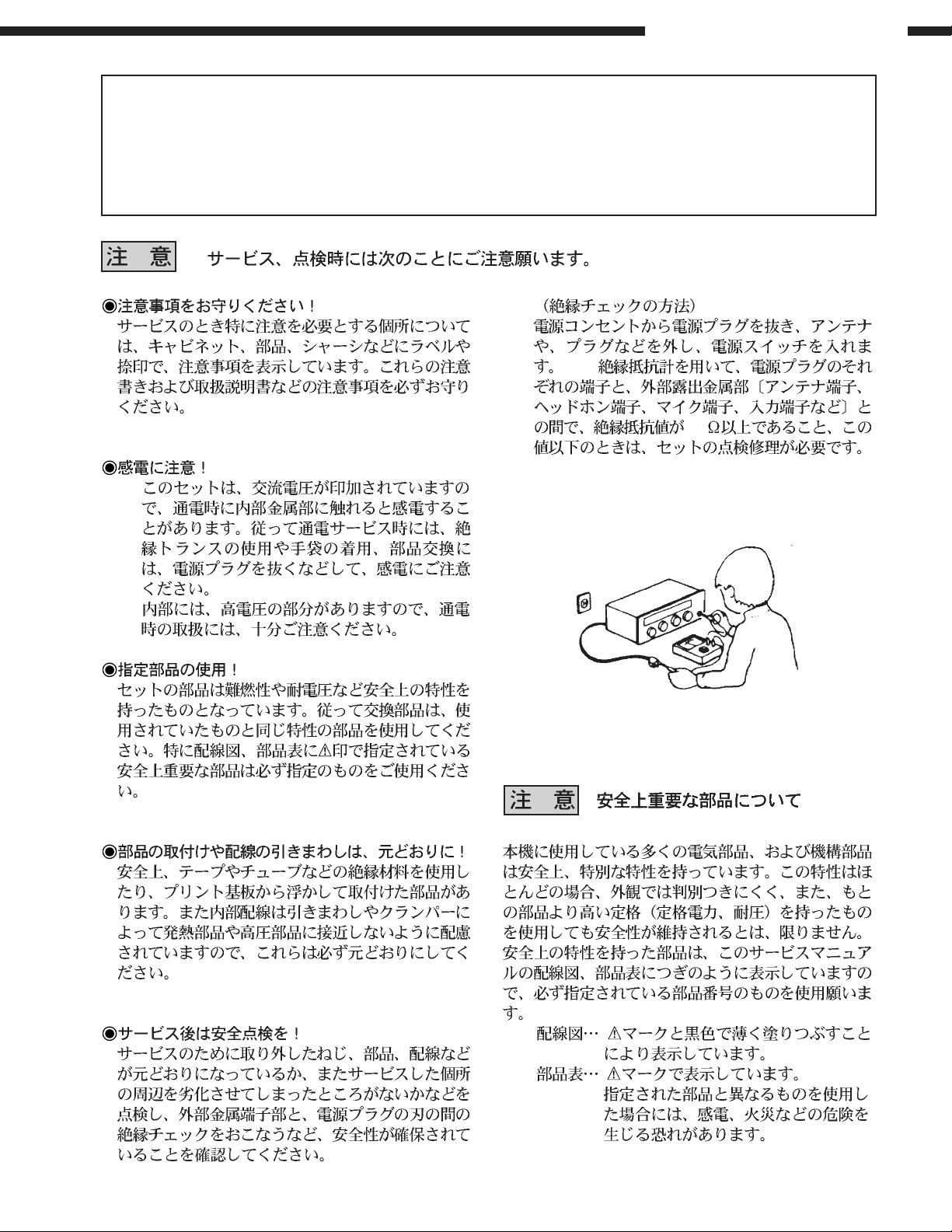
SAFETY PRECAUTIONS
The following check should be performed for the continued protection of the customer and service technician.
LEAKAGE CURRENT CHECK
Before returning the unit to the customer, make sure you make either (1) a leakage current check or (2) a line to chassis
resistance check. If the leakage current exceeds 0.5 milliamps, or if the resistance from chassis to either side of the
power cord is less than 460 kohms, the unit is defective.
500V
1M
(1)
(2)
(1)
(2)
2

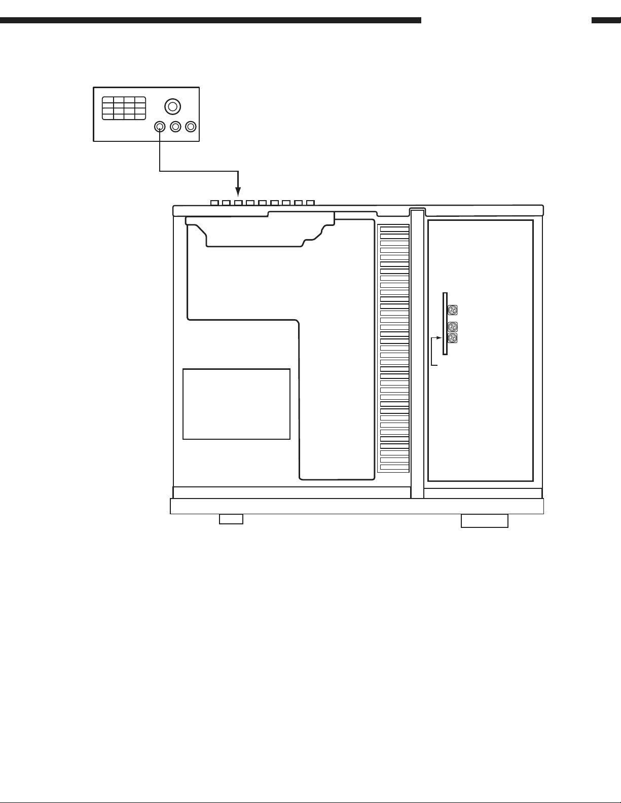
WIRE ARRANGEMENT
If wire bundles are untied or moved to perform adjustment or
parts replacement etc.,be sure to rearrange them neatly as
they were originally bundled or placed afterward.
Otherwise, incorrect arrangement can be a cause of noise
generation.
Wire arrangement viewed from the top
AVR-3803/1083/AVC-3570
3

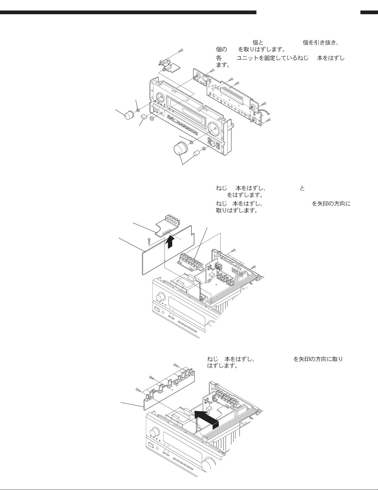
DISASSEMBLY
(Follow the procedure below in reverse order
when reassembling)
AVR-3803/1083/AVC-3570
1. Top Cover
Remove 3 screws on the rear and 6 screws on both
sides to detach the Top Cover as shown in the arrow
direction.
Top Cover
2. Front Panel
(1) Remove 7 screws from the top and bottom edges of
the Front Panel.
(2) Release 4 top and bottom Hooks, then detach the
Front Panel as shown in the arrow direction.
1. Top Cover
3 6 Top Cover
2. Front Panel
(1) Front Panel 7
(2) Front Panel 4 Hook
Front Panel
Hook
Front Panel
Hook
3. Inner Panel
Pull out the Inner Panel in the arrow direction after
removing 3 screws.
Inner Panel
Hook
3. Inner Panel
3 Inner Panel
Hook
4
AVR-3803/1083/AVC-3570
4. Inner Panel Ass'y
(1) Remove 3 round and 1 square knobs, and unscrew 4
nuts.
(2) Remove 14 screws fixing each P.W.B.
Nut
Round Knob
Square Knob
Nut
Round Knob
5. Amp Connect Unit/Component Video Unit
(1) Remove 9 screws to detach Pre-out Unit and
Component Video Unit.
(2) Take off the Amp Connect Unit as shown in the arrow
direction after removing 1 screw.
Pre-out Unit
Amp Connect Unit
4. Inner Panel Ass'y
(1) Round Knob 3 Square Knob 1 4
Nut
(2) PWB 14
5. Amp Connect Unit/Component Video Unit
(1) 12 Pre-out Unit Component Video
Unit
(2) 1 Amp Connect Unit
Component Video Unit
6. Regulator Unit
Take off the Regulator Unit as shown in the arrow
direction after removing 11 screws.
Regulator Unit
6. Regulator Unit
11 Regulator Unit
5
AVR-3803/1083/AVC-3570
7. Component-Video/S-Video / C-video /
Audio in / Ext-in VR / Digital/Remote I/O
/ AM FM Tuner Unit
(1) Remove 60 screws to detach the Rear Panel.
(2) Take off the objective P.W.B. upward.
Rear Panel
7. Component-Video/S-Video / C-video /
Audio in / Ext-in VR / Digital/Remote I/O
(1) 61 Rear Panel
(2) P.W.B.
8. How to Check Power / Control Unit with
Power-on
(1) Remove 17 screws fixing to the Chassis.
(2) Pull up the Unit to separate from the Chassis.
8. Powr/Control Unit
(1) Chassis 17
(2) Chassis
Chassis
6
CAUTION IN SERVICING
AVR-3803/1083/AVC-3570
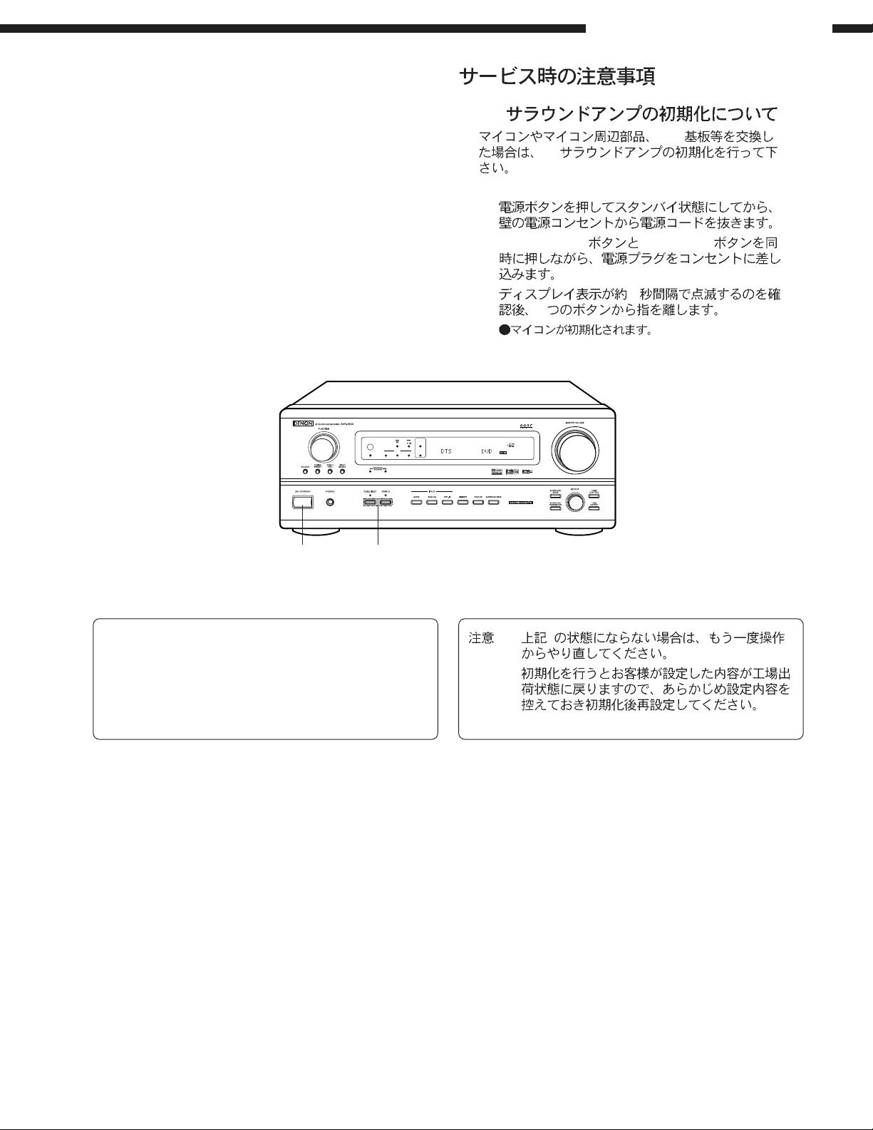
Initializing AV SURROUND RECEIVER
AV SURROUND RECEIVER initialization should be
performed when the µcom, peripheral parts of µcom, and
DSP P.W.B. are replaced.
1. Switch off the unit and remove the AC cord from the
wall outlet.
2. Hold the following PURE DIRECT button and ZONE
2 button, and plug the AC cord into the outlet.
3. Check that the entire display is flashing with an
interval of about 1 second, and release your fingers
from the 2 buttons and the microprocessor will be
initialized.
REMOTE
SIGNAL
SENSOR
DIGITAL
INPUT
ON / STANDBY
AUTO
DTS
PCM
AV
DSP
AV
1.
2. PURE DIRECT VIDEO OFF
3. 1
2
SURROUND
BACK CH
OUTPUT
SIGNAL
DETECT
VOLUME LEVEL
1 2
Note: If step 3 does not work, start over from step 1.
All user settings will be lost and this factory
setting will be recovered when this initialization
mode.
So make sure to memorize your setting for
restoring after the initialization.
: 3 1
7
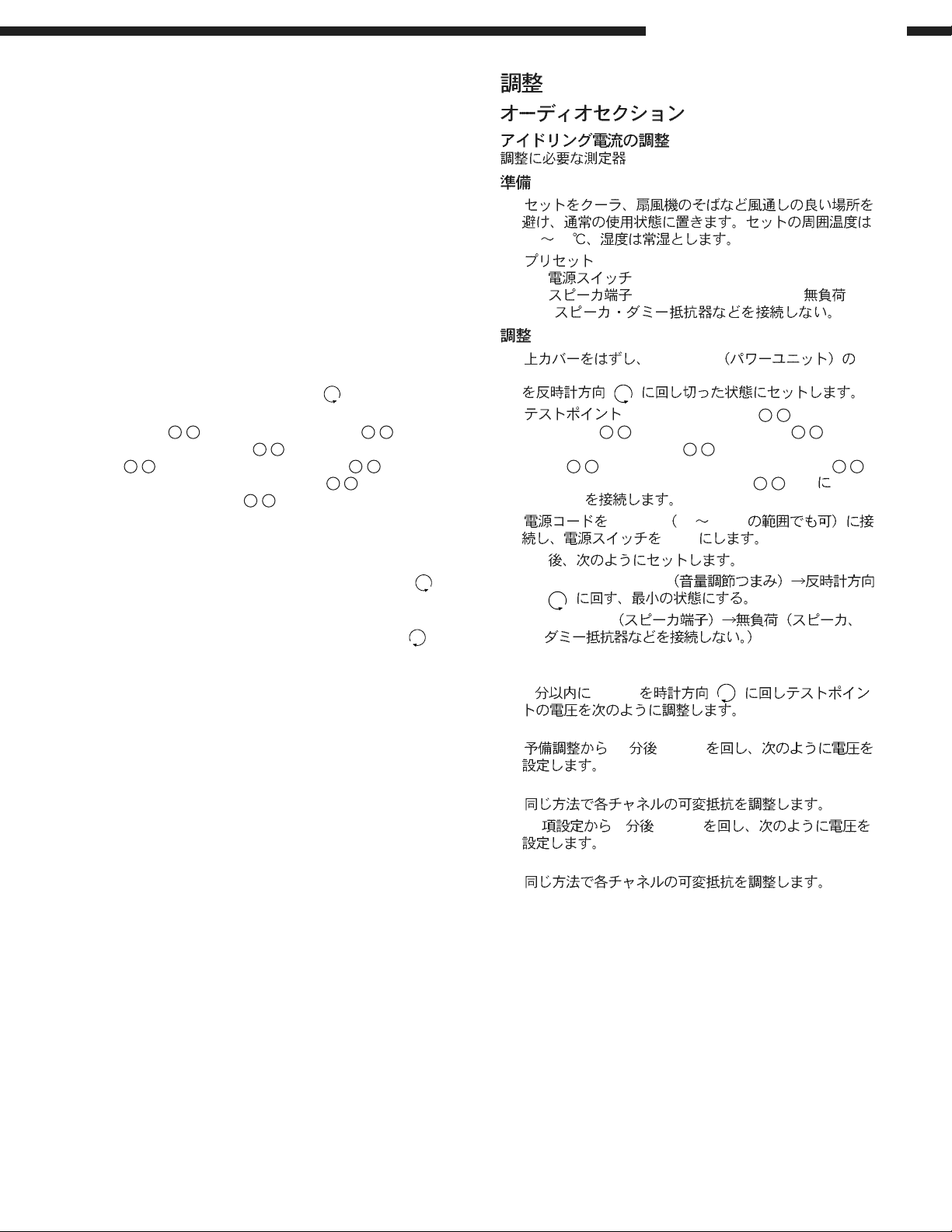
ADJUSTMENT
Audio Section
Idling Current (1U-3469-1)
Required measurement equipment: DC Voltmeter
Preparation
(1) Avoid direct blow from an air conditioner or an electric
fan, and adjust the unit at normal room tempereture 15
°C ~ 30 °C (59 °F ~ 86 °F).
(2) Presetting
POWER (Power sourse switch) OFF
SPEAKER (Speaker terminal) No load
(Do not connect speaker, dummy resistor, etc.)
Adjustment
(1) Remove top cover and set VR101, VR102, VR201,
VR301, VR302, VR401, VR402, on 1U-3469-1 (Power
Unit) at fully counterclockwise ( ).
(2) Connect DC Voltmeter to test points (FRONT-Lch:
1 2
TP301
CENTER ch: TP301 3 4 pin, SURROUND-Lch: TP101
3 4
SURROUND BACK-Lch: TP301
BACK-Rch: TP301 5 6 pin).
(3) Connect power cord to AC Line, and turn power switch
"ON".
(4) Presetting.
MASTER VOLUME : "---" counterclockwise ( min.)
MODE : 7CH STEREO
FUNCTION : CD
(5) Allow 2 minutes, and turn VR101 clockwise ( ) to
adjust the TEST POINT voltage to 6.5 mV ±0.5 mV DC.
(6) After 10 minutes from preset, turn VR101 to set the
voltage to 8 mV ±0.5 mV DC.
(7) Adjust the Variable Resistors of other channels in the
same way.
(8) After 5 minutes from (6), turn VR101 to set the voltage to
8 mV ±0.5 mV DC.
(9) Adjust the Variable Resistors of other channels in the
same way.
pin, FRONT-Rch: TP101 5 6 pin,
pin, SURROUND-Rch: TP101 1 2 pin,
7 8
pin, SURROUND
AVR-3803/1083/AVC-3570
(1U-3469-1)
: DC Voltmeter
(1)
15 30
(2)
OFF
( )
(1) 1U-3469-1
VR101, VR102, VR201, VR301, VR302, VR401, VR402
( )
(2) (FRONT-Lch: TP301 1 2 pin, FRONT-
5 6
Rch: TP101
SURROUND-Lch: TP101 3 4 pin, SURROUND-Rch:
TP101 1 2 pin, SURROUND BACK-Lch: TP301 7
pin, SURROUND BACK-Rch: TP301 5 6 pin) DC
Voltmeter
(3) AC100V 95 105V
(4) ON
MASTER VOLUME
( )
SPEAKER
(5) 2 VR101 ( )
(6) 10 VR101
(7)
(8) (6) 5 VR101
pin, CENTER ch: TP301 3 4 pin,
8
"ON"
MODE : 7CH STEREO
FUNCTION : CD
6.5mV ±0.5mV DC
8mV ±0.5mV DC
(9)
8mV ±0.5mV DC
8

DC Voltmeter
SR ch
VR302
SL ch
VR301
FR ch
VR102
FL ch
VR101
C ch
VR201
SBR ch
VR402
SR ch
SL ch
FR ch
FL ch
C ch
SBR ch
SBL ch
AVR-3803/1083/AVC-3570
TP101
TP301
SBL ch
VR401
Audio Section
9
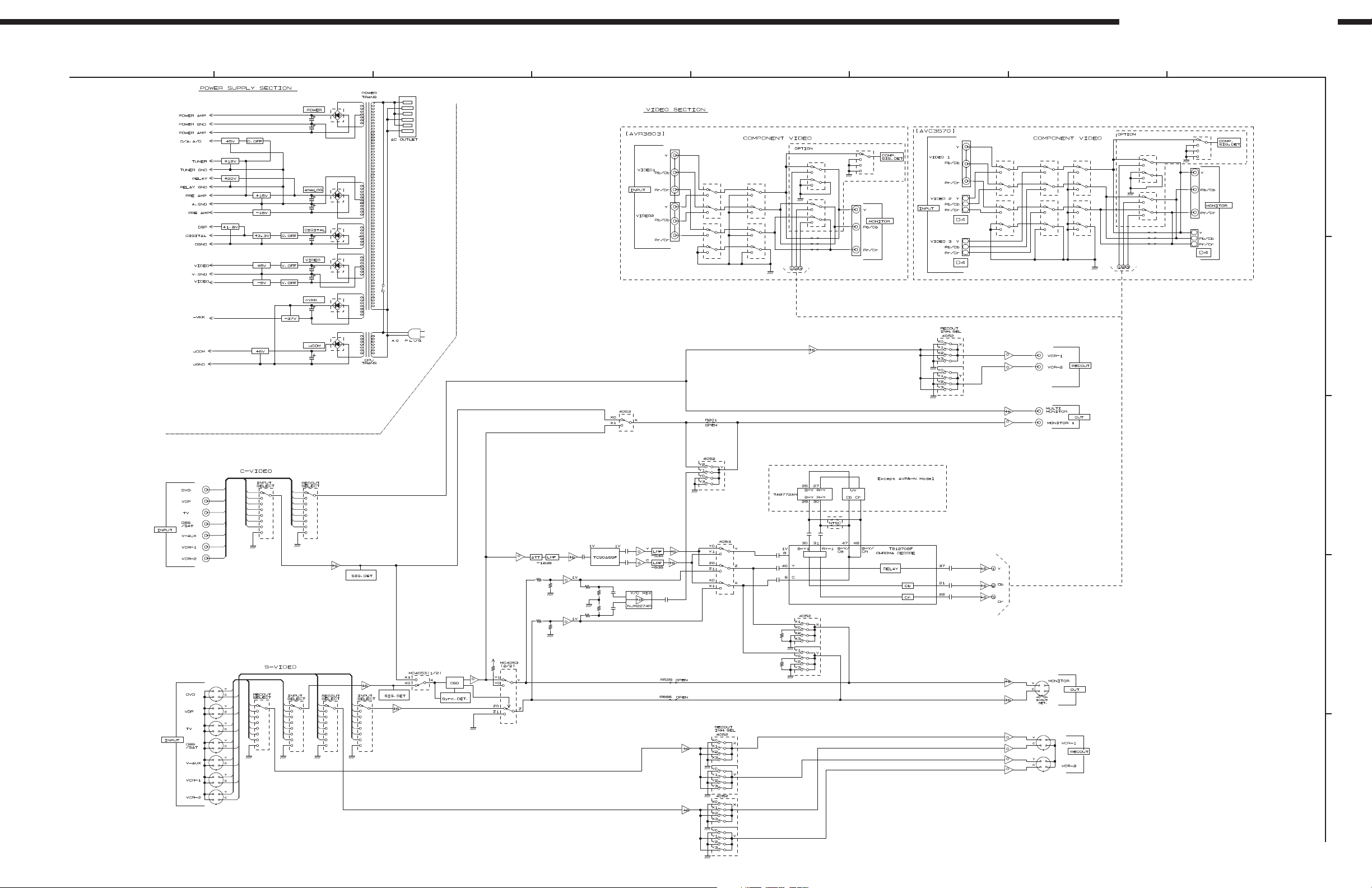
Video Section
Component Video Level Adjustment
Required measurement equipment etc: Oscilloscope, DVD
VIDEO PLAYER (ex: DVD-1500)
Test Disc: DVD T-S01
Preparation
(1) Avoid direct blow from an air conditioner or an electric
fan, and adjust the unit at normal room temperature 15
°C ~ 30 °C (59 °F ~ 86 °F).
(2) Playback the color-bar 75% of the Test Disc (Title 12)
using the DVD Video Player, and check that Y and C
levels of the S terminal output are within the specified
output levels.
If they are out of the specified levels, adjust with the
variable resister inside of the unit.
(3) Presetting
POWER (Power source switch) OFF
SPEAKER (Speaker terminal) No load
(Do not connect speaker, dummy resistor, etc.)
DVD (Video terminal) No input
Adjustment
(1) Remove top cover and set VR101, VR102, VR103 on
1U-3475-1 (Convert Unit) at fully counterclockwise (
(2) Connect a pin-plug terminated with 75-ohms to Y(Cb,
Cr) of the Component Video Monitor Output, and hook
up the Oscilloscope's probe to both ends of the pin-plug.
(3) Connect S terminal output of the DVD Player with the
DVD input terminal of the Receiver.
(4) Connect power cord to AC Line, and turn power switch
"ON".
(5) Presetting
FUNCTION: DVD
Playback the color-bar 75% of the Test Disc (Title 12)
(6) Turn VR101 clockwise ( ) to adjust the
COMPONENT VideoY voltage (except H.Sync) to 714
±50 mVp-p. (Refer to Fig.1)
(7) Adjust the Variable Resistors of Cb: VR102 and Cr:
VR103 in the same way. (Refer to Fig. 2, 3)
Cb,Cr: 486±50 mVp-p. (U.S.A. & Canada model)
525±50 mVp-p. (Others)
AVR-3803/1083/AVC-3570
: Oscilloscope, DVD VIDEO PLAYER
( : DVD-1500)
: DVD T-S01
(1)
15 30
(2) DVD VIDEO PLAYER
75 (Title12) S Y C
(3)
OFF
( )
DVD
(1) 1U-3475-1
).
VR101, VR102, VR103 ( )
(2) Y(Cb, Cr) 75
Oscilloscope
(3) DVD VIDEO PLAYER S DVD
(4)
"ON"
(5) ON
FUNCTION DVD
75 (Title12)
(6) VR101 ( )
Y(H.Sync ) (Fig.1 )
714mV ±50mVp-p
(7) Cb: VR102 Cr: VR103
(Fig.2 3 )
Cb,Cr: 525±50 mVp-p.
10
Oscilloscope
AVR-3803/1083/AVC-3570
VR103Cr
Cb
VR102
VR101
Video Section
Component Video Y
11
AVR-3803/1083/AVC-3570
Volts
IRE:FLT
100.0
0.5
0.0
0.5
-20.0 -10.0 0.0
Volts
IRE:FLT
0.5
50.0
Y-Signal
714±50mV
p-p
10.0
20.0 30.0
Fig.1 Component Video Y signal
40.0 50.0 60.0
486±50mV (U.S.A. & Canada model)
p-p
525±50mV (Others)
p-p
0.0
-0.5
Volts
0.5
0.0
0.0
-50.0
0.0
IRE:FLT
50.0
0.0
-50.0
20.0
Fig.2 Cb signal
40.0
60.0
486±50mV (U.S.A. & Canada model)
525±50mV (Others)
80.0
p-p
p-p
-0.5
0.0
20.0
Fig.3 Cr signal
40.0
60.0
80.0
12
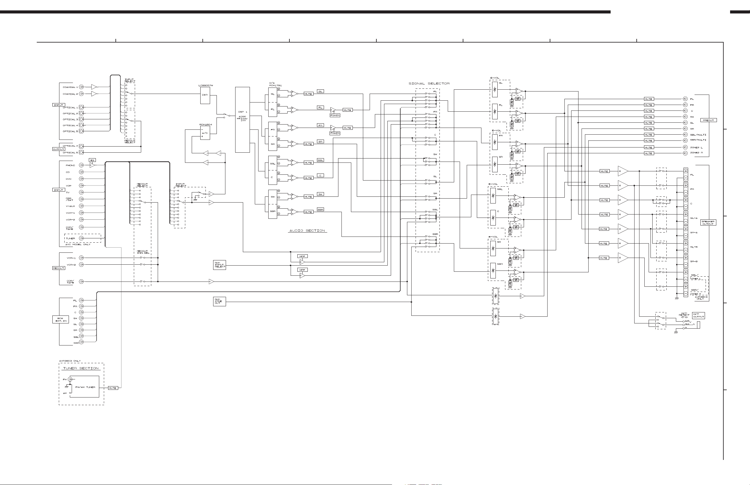
BLOCK DIAGRAMS (1/2)
AVR-3803/AVR-1083/AVC-3570
1
2
3
4
5
76
8
A
B
C
D
E
13
BLOCK DIAGRAMS (2/2)
AVR-3803/AVR-1083/AVC-3570
1
2
3
4
5
76
8
A
B
C
D
E
14
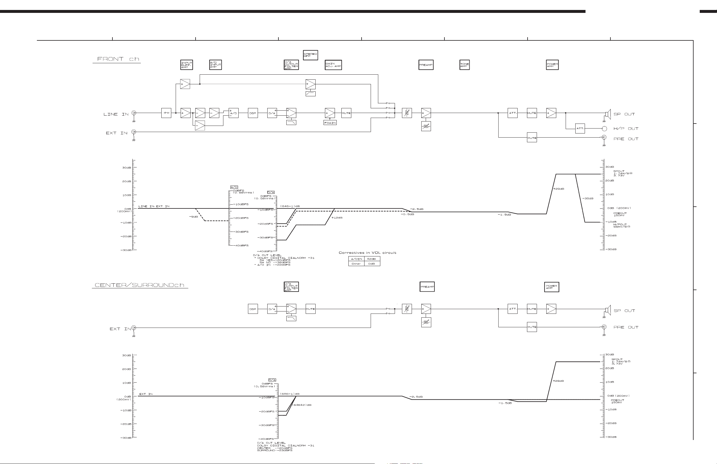
LEVEL DIAGRAMS (1/5)
AVR-3803/AVR-1083/AVC-3570
1
AUDIO SECTION (1/2)
2
3
4
5
76
8
A
B
C
D
E
15
LEVEL DIAGRAMS (2/5)
AVR-3803/AVR-1083/AVC-3570
1
AUDIO SECTION (2/2)
2
3
4
5
76
8
A
B
C
D
E
16
LEVEL DIAGRAMS (3/5)
AVR-3803/AVR-1083/AVC-3570
1
VIDEO SECTION (1/3)
2
3
4
5
76
8
A
B
C
D
E
17
LEVEL DIAGRAMS (4/5)
AVR-3803/AVR-1083/AVC-3570
1
VIDEO SECTION (2/3)
2
3
4
5
76
8
A
B
C
D
E
18
LEVEL DIAGRAMS (5/5)
AVR-3803/AVR-1083/AVC-3570
1
VIDEO SECTION (3/3)
2
3
4
5
76
8
A
B
C
D
E
19
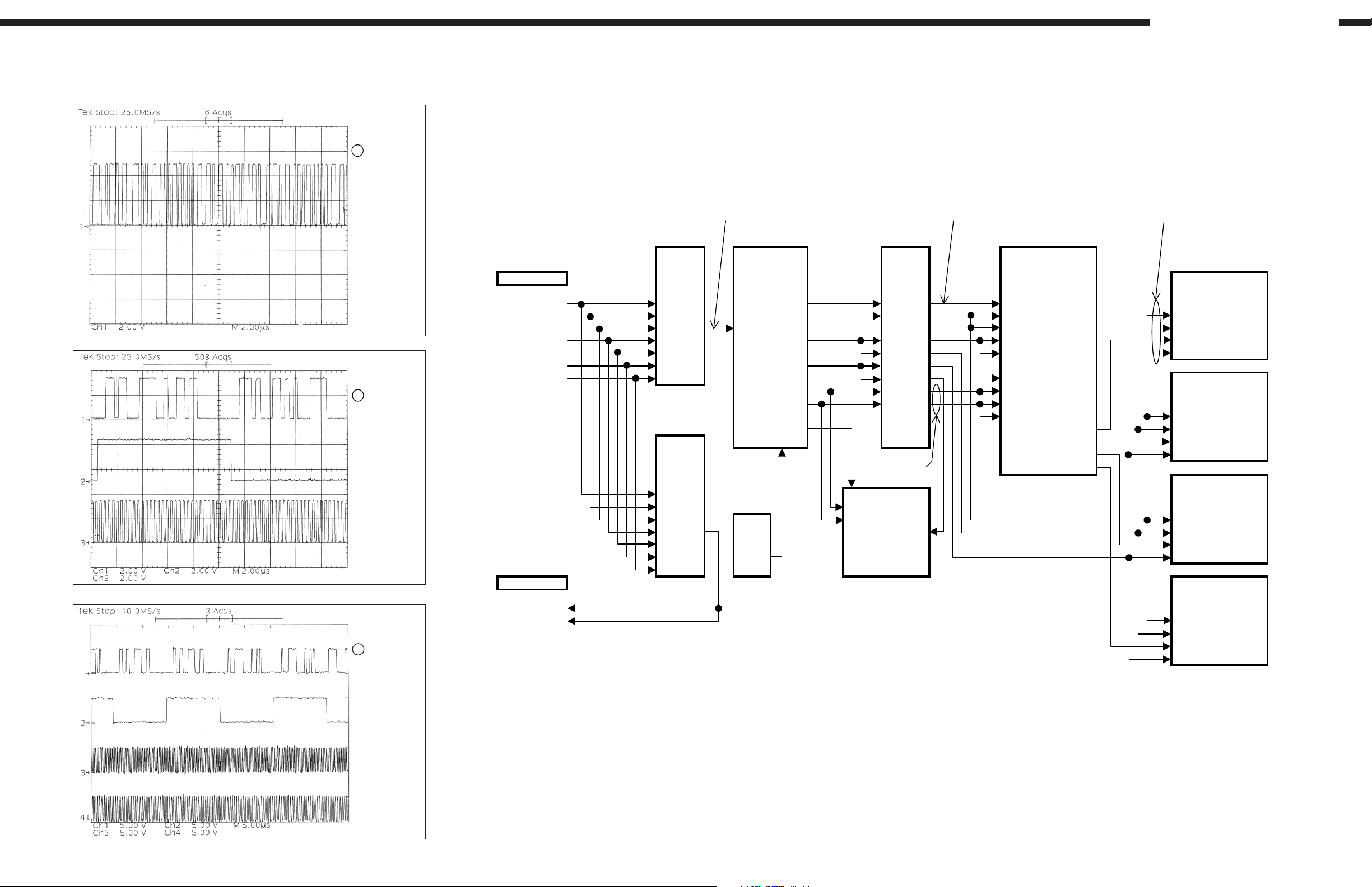
CLOCK FLOW & WAVE FORM IN DIGITAL BLOCK
㽳㽳
㽴㽴
㽳㽳㽳㽳
/
Wave form
1
CH1: D-DATA
(IC510 (5) )
AVR-3803/1083/AVC-3570
2
CH1: DATA
CH2: fs
CH3: 64fs
3
CH1: DATA
㽲㽲㽲㽲㽳
INPUT
INPUT
INPUTINPUT
SELECTOR
SELECTOR BUFFER
SELECTORSELECTOR
IC5㪈3
IC5㪈3 IC522
IC5㪈3IC5㪈3
INPUT
INPUT
INPUTINPUT
COAXIAL-㪈
COAXIAL-㪈 (3) RDATA(2㪈)(㪈㪈)- -(9) (64)SD0A
COAXIAL-㪈COAXIAL-㪈
COAXIAL-2
COAXIAL-2 (2) SLRCK(23) (㪈3)- -(7) (38)SFS2 (㪈)fs
COAXIAL-2COAXIAL-2
OPTICAL-㪈
OPTICAL-㪈 (㪈2) (5) (4)RX2 (39)SFS3 (2)64fs SLch
OPTICAL-㪈OPTICAL-㪈
OPTICAL-2
OPTICAL-2 (㪈3) SBCK(22) (㪈5)- -(5) (7)SCLK2 (3)DATA FLch
OPTICAL-2OPTICAL-2
OPTICAL-3
OPTICAL-3 (㪈4) (㪈7)- -(3) (54)SCLK3 (5)256fs
OPTICAL-3OPTICAL-3
OPTICAL-4
OPTICAL-4 (㪈5) RMCK(㪈6) (4)- -(㪈6)
OPTICAL-4OPTICAL-4
OPTICAL-5
OPTICAL-5 (㪈) (2)- -(㪈8) (50)SCLK0
OPTICAL-5OPTICAL-5
SN74HC
SN74HC SN74LV
SN74HC SN74HC
㪈5㪈APW
㪈5㪈APW 244APW
㪈5㪈APW㪈5㪈APW
OUTPUT
OUTPUT (52)SFS㪈 (㪈)fs
OUTPUTOUTPUT
SELECTOR
SELECTOR ADIN(24) SD2A(37) (2)64fs FRch
SELECTORSELECTOR
DIR
DIR DSP
DIRDIR
IC520
IC520
IC520IC520
LC89057W
LC89057W
LC89057WLC89057W
DATA
fs
64fs
256fs
RBCK(㪈7) (6)- -(㪈4) (2㪈)SCLK㪈
RLRCK(20) (8)- -(㪈2) (20)SFS0
64fs
fs
BUFFER
BUFFERBUFFER
IC522
IC522IC522
SN74LV
SN74LVSN74LV
244APW
244APW244APW
㽳㽴
DSP
DSPDSP
IC80㪈
IC80㪈
IC80㪈IC80㪈
ADSST-MEL㪈00
ADSST-MEL㪈00
ADSST-MEL㪈00ADSST-MEL㪈00
㽴
D/A CONVERTER
D/A CONVERTER
A CONVERTERD/A CONVERTER
D
IC523
IC523
IC523IC523
PCM㪈79㪈
PCM㪈79㪈
PCM㪈79㪈PCM㪈79㪈
IC524
IC524
IC524IC524
PCM㪈79㪈
PCM㪈79㪈
PCM㪈79㪈PCM㪈79㪈
(29)XIN SD2B(22) (3)DATA SRch
IC5㪈4
IC5㪈4 SD3A(23) (5)256fs
IC5㪈4IC5㪈4
SN74HC
SN74HC
SN74HC SN74HC
㪈5㪈APW
㪈5㪈APW
㪈5㪈APW㪈5㪈APW
(3) (㪈5)DATA
(2) 24.576MHz
(㪈2) IC52㪈
(㪈3) (5) FXC0
(㪈4) -03
(㪈5) (3) (5)256fs
(㪈)
OUTPUT
OUTPUT
OUTPUTOUTPUT
OPTICAL-4
OPTICAL-4
OPTICAL-4OPTICAL-4
OPTICAL-5
OPTICAL-5 (㪈)fs
OPTICAL-5OPTICAL-5
24.576MHz (㪈6)BCK
24.576MHz24.576MHz
IC52㪈 (㪈7)LRCK (㪈)fs
IC52㪈IC52㪈
FXC0 SYSCK(㪈8) (2)64fs SBLch
FXC0FXC0
-03 (3)DATA Cch
-03-03
IC5㪈9
IC5㪈9
IC5㪈9IC5㪈9
PCM㪈804
PCM㪈804
PCM㪈804PCM㪈804
A/D CONVERTER
A/D CONVERTER IC526
A/D CONVERTERA/D CONVERTER
SD3B (8)
IC525
IC525
IC525IC525
PCM㪈79㪈
PCM㪈79㪈
PCM㪈79㪈PCM㪈79㪈
IC526
IC526IC526
PCM㪈79㪈
PCM㪈79㪈
PCM㪈79㪈PCM㪈79㪈
(2)64fs SWch
(3)DATA SBRch
(5)256fs
CH2: fs
CH3: 64fs
CH4: 256fs
20
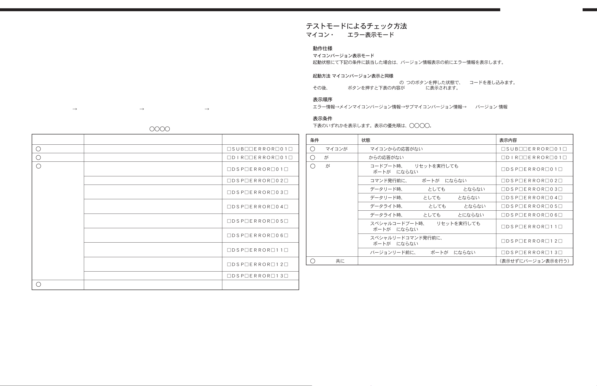
CHECK WITH TEST MODE
µµ
µcom/DSP Error Display Mode
µµ
AVR-3803/1083/AVC-3570
DSP
1. Operation Spec
µµ
µcom version display mode:
µµ
When the following conditions are satisfied at its starting state, error information is displayed before version information.
Starting method (same as
While pressing 2 buttons, "DIMMER (S11)" and "SURROUND BACK (S14)", plug the AC cord to the wall outlet.
Then, press "STATUS" button to display the following information on the FL Display.
µµ
µcom version display):
µµ
2. Display Order
Error information Main-µcom version information Sub-µcom version information DSP version information
3. Display
1
2 3
Any one of the following list is displayed, in the priority of
Condition State Display
1
Sub-µcom NG No response from Sub-µcom " "
2
DIR NG No response from DIR " "
3
DSP NG When DSP boot, executing DSP reset
makes no change to BUSY port "L".
No change to BUSY port "L" before issuing DSP command. " "
When DSP data read, executing WRITE="L"
makes no change to ACK="H".
When DSP data read, executing REQ="L"
makes no change to ACK="L".
When DSP data write, executing WRITE="H"
makes no change to ACK="H".
When DSP data write, executing REQ="L"
makes no change to ACK="L".
When DSP special code boot, executing DSP reset
makes no change to BUSY port "L".
No change to BUSY port "L" before issuing
DSP special read command.
4
.
"
"
"
"
"
"
"
1.
:
( ):
"DIMMER"(S11), "SURROUND BACK"(S14)
STATUS FL Display
2 AC
2.
DSP
3.
1 234
1
SUB NG SUB " "
2
DIR NG DIR " "
3
"
"
"
"
"
"
"
DSP NG DSP DSP
BUSY "L"
DSP BUSY "L" " "
DSP WRITE="L" ACK="H" " "
DSP REQ="L" ACK="L" " "
DSP WRITE="H" ACK="H" " "
DSP REQ="L" ACK="L" " "
DSP
BUSY "L"
DSP
BUSY "L"
DSP BUSY "L" " "
4
SUB/DSP OK
DSP
" "
" "
" "
4
Both SUB/DSP OK
No change to BUSY port "L" before DSP version read. " "
(No error display, version display only)
21
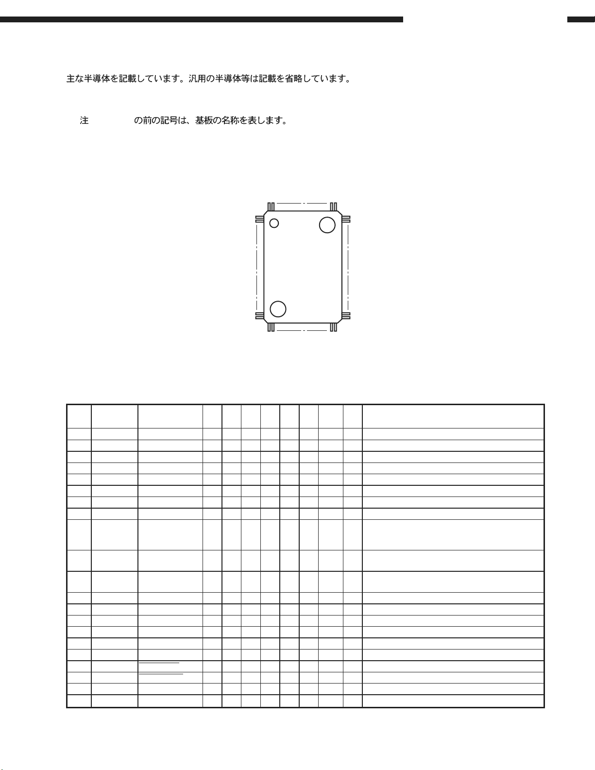
SEMICONDUCTORS
Only major IC's are shown, general IC's etc. are omitted to list.
IC’s
Note: Abbreviation ahead of IC No. indicates the name of P.W.B., etc.
) : IC No.
PO : Power P.W.B. AD : Audio/Digital P.W.B.
CV : Connect/Video P.W.B. DS : DSP P.W.B.
CO: Control P.W.B. VI : Video P.W.B.
AC : Amp Connect P.W.B. MA: Main Sub Ass'y
M30624MGA (CO: IC506)
100 81
AVR-3803/1083/AVC-3570
1
TOP VIEW
30
31 50
80
51
M30624MGA Terminal Function
Pin
Pin Name FunctionI/O
No.
1 P96/SOUT4 PLRDS DATA O C Z O/L O/L PLL & RDS control pin (LC72131 & LC72720)
2 P95/CLK4 PLRDS CLK O C Z O/L O/L PLL & RDS control pin (LC72131 & LC72720)
3 P94/TB4 PLL STB O C Z O/L O/L PLL control pin (LC72131)
4 P93/TB3 OSD RST O C Z O/L O/L OSD control pin (M35015)
5 P92/SOUT3 OSD DATA O C Z O/L O/L OSD control pin (M35015)
6 P91/SIN3 OSD STB O C Z O/L O/L OSD control pin (M35015)
7 P90/CLK3 OSD CLK O C Z O/L O/L OSD control pin (M35015)
8 BYTE BYTE GND (Ext. data bus bit width switching, 16bit: L)
9 CNVCS CNVSS
10 P87 ISEL B I Lv Eu Z O/L O/L
11 P86 ISEL A I Lv Eu Z O/L O/L
12 RESET _RESET I Lv Eu L I I Reset input
13 XOUT X1 O Oscillator connection
14 VSS VSS GND
15 XIN X2 I I I Oscillator connection
16 VCC VCC +5V
17 P85/NMI _NMI I Not used (Fixed to H)
18 P84/INT2 _B. DOWN I
19 P83/INT1 _PROTECT I
20 P82/INT0 REMOCON I
21 P81 VSEL A I Lv Eu Z I O/L Master VR rotation detect input (Rotary encoder)
Symbol
Type
Op
Det
(Int.)Op(Ext.)
E↓&L
Eu Z I I Power down detect (Power down: L)
E↓&L
Ed Z I I Protection detect input (Detected: L)
E↑&L
Z I I Remote control signal input
Re s STBY Stop
Single-chip/Micro-processor mode switching
(Normal single-chip: L, Rewrite boot program start:
H input set)
Input selector rotation detect input
(Rotary encoder)
Input selector rotation detect input
(Rotary encoder)
22
AVR-3803/1083/AVC-3570
Pin
Pin Name FunctionI/OSymbol
No.
22 P80 VSEL B I Lv Eu Z I O/L Master VR rotation detect input (Rotary encoder)
23 P77 FUNC STB1 O C Z O/L O/L
24 P76 FUNC CLK O C Z O/L O/L CLK output for function switching control
25 P75 FUNC DATA O C - Z O/L O/L DATA output for function switching control
26 P74 FUNC STB2 O C Z O/L O/L
27 P73/CTS2 FL DATA O C Z O/L O/L FL tube control pin (LC75721E)
28 P72/CLK2 FL CLK O C Z O/L O/L FL tube control pin (LC75721E)
29 P71/RXD2 H/P DET I Z O/L O/L H/P detect input (Detected: H)
30 P70/TXD2 TUNER POWER O N Eu Z O/L O/L TUNER power on/off switching (H: ON)
31 P67/TXD1 TxD O C Z O/L O/L Data transfer pin to outside
32 P66/RXD1 RxD I Lv Z I I Data receive pin from outside
33 P65/CLK1 RESET2 O C Ed Z O/L O/L SUB-µcom reset output
34 P64/CTS1 ACK O C Ed Z O/L O/L MAIN-SUB µcom comm. control pin
35 P63/TXD0 MOSI O C Ed Z O/L O/L MAIN-SUB µcom comm. control pin
36 P62/RXD0 MISO I Lv Ed Z I I MAIN-SUB µcom comm. control pin
37 P61/CLK0 Not Used (CLK) O C Z O/L O/L Not used
38 P60/CTS0 E.VOL STB O C Z O/L O/L E-VR control output (TC94A32F)
39 P57 E.VOL CLK O C Z O/L O/L E-VR control output (TC94A32F, TC9459)
40 P56 E.VOL DATA O C Z O/L O/L E-VR control output (TC94A32F, TC9459)
41 P55/EPM FRASH EPM I Lv Z I I Rewrite boot program start: L input set
42 P54 VSDA I/O C Z I O/L VIDEO IC (Chroma decoder, 3D Y/C) control pin
43 P53 VSCL I/O C Z I O/L VIDEO IC (Chroma decoder, 3D Y/C) control pin
44 P52 FL RST O C Ed Z O/L O/L FL tube control pin (LC75721E)
45 P51 FL CE O C Z O/L O/L FL tube control pin (LC75721E)
46 P50/CE FRASH CE I Z I I Rewrite boot program start: H input set
47 P47 V.EXP CLK O C Z O/L O/L
48 P46 V.EXP DATA O C Z O/L O/L
49 P45 V.EXP OE O C Ed Z O/L O/L
50 P44 V.EXP STB O C Z O/L O/L
51 P43 H/P RELAY O C Z O/L O/L H/P relay control (H: ON)
52 P42 S BACK RELAY O C Z O/L O/L Relay control for SURROUND BACK SP
53 P41 SA-RELAY O C Z O/L O/L Relay control for SURROUND A SP
54 P40 SB-RELAY O C Z O/L O/L Relay control for SURROUND B SP
55 P37 C-RELAY O C Z O/L O/L Relay control for CENTER SP
56 P36 F-RELAY O C Z O/L O/L Relay control for FRONT SP
57 P35 PRE F MUTE O C Z O/L O/L FRONT PREOUT output muting control, L: Muting
58 P34 PRE C MUTE O C Z O/L O/L
59 P33 PRE S MUTE O C Z O/L O/L
60 P32 PRE SB MUTE O C Z O/L O/L
61 P31
62 VCC VCC +5V
63 P30 MULTI MUTE O C Z O/L O/L Pin-jack output muting control of MULTI, L: Muting
64 VSS VSS GND
65 P27 VOL MUTE O C Z O/L O/L POWER AMP input muting control, L: Muting
66 P26
67 P25 TUNER MUTE O C Z O/L O/L TUNER muting control
SUB WOOFER MUTE
S.BACK VOL MUTE
Type
OC Z O/L O/L
OC Z O/L O/L
Det
Op
(Int.)Op(Ext.)
Re s STBY Stop
STB output for function switching control
(L-ch INPUT&REC/M-ZONE side, EXT IN)
STB output for function switching control
(R-ch INPUT&REC/M-ZONE)
CLK output for video switching expander control
(BU4094B)
DATA output for video switching expander control
(BU4094B)
OE output for video switching expander control
(BU4094B)
STB output for video switching expander control
(BU4094B)
CENTER PREOUT output muting control,
L: Muting
SURROUND PREOUT output muting control,
L: Muting
SURROUND BACK PREOUT output muting
control, L: Muting
SUB WOOFER PREOUT output muting control,
L: Muting
SURROUND BACK POWER AMP input muting
control, L: Muting
23
AVR-3803/1083/AVC-3570
Pin
Pin Name FunctionI/OSymbol
No.
68 P24 LED CLK O C Z O/L O/L LED control pin (BU2090F)
69 P23 LED DATA O C Z O/L O/L LED control pin (BU2090F)
70 P22 S MONI. DET I Lv Eu Z I O/L S-monitor connection detect input (L: Connected)
71 P21 S SIG. DET I Lv Eu Z I O/L S-signal detect input (H: S-signal inputted)
72 P20 SYNC. DET I Lv Eu Z I I Sync. detect input (H: Ext. synchronized)
73 P17/INT5 RDS DATAOUT I
74 P16/INT4 REQ I
75 P15/INT3 POWER KEY I
76 P14/D12 RSPOWER O C Ed Z O/H O/L
77 P13/D11 RECINHA O C Z O/L O/L
78 P12/D10 SSEL B I Lv Eu Z O/L O/L
79 P11/D9 SSEL A I Lv Eu Z O/L O/L
80 P10/D8 A+B LIMIT O C Z O/L O/L
81 P07/D7 VSIGDET I Z O/L O/L VIDEO signal detect port
82 P06/D6 COMPSIGDET I Z O/L O/L COMPONENT signal detect port
83 P05/D5 VIDEO POWER O C Z O/L O/L VIDEO power on/off switching (H: ON)
84 P04/D4 12V TRIGER O C Z O/L O/L
85 P03/D3
86 P02/D2 RECINHB O C Z O/L O/L When RECOUT select is VCR1 or VCR2: H
87 P01/D1 POWER O C Ed Z O/L O/L Power relay control output (H: ON)
88 P00/D0 STANDBY O C Eu Z O/L O/L Standby LED drive output (H: Lighted)
89 P107/AN7 KEY1 I Lv Eu Z O/L O/L Button input 1
90 P106/AN6 KEY2 I Lv Eu Z O/L O/L Button input 2
91 P105/AN5 KEY3 I Lv Eu Z O/L O/L Button input 3
92 P104/AN4 STEREO I Lv Eu Z I O/L When TUNER FM stereo receive: L
93 P103/AN3 TUNED I Lv Eu Z I O/L TUNER tuned detect (L: Tuned)
94 P102/AN2 RDS CE O C Z O/L O/L RDS data output (LC72720)
95 P101/AN1 RDS RESET O C Z O/L O/L RDS reset output (LC72720)
96 AVSS AVSS AD GND
97 P100/AN0 MODE I Lv Z O/L O/L Destination switching input
98 VREF VREF AD ref. +5V
99 AVCC AVCC AD +5V
100 P97/SIN4 PLL DATAOUT I Lv Z I O/L PLL serial data input pin (LC72131)
E.VOL STB.MULTI
Type
OC Z O/L O/L E-VR control output (TC9459N)
Op
Det
(Int.)Op(Ext.)
E↓&L
I O/L RDS data input (LC72720)
E↓&L
Ed Z I I MAIN-SUB µcom comm. control pin
E↓&L
I O/L Interrupt port for WAIT mode cancel
Re s STBY Stop
Same logic as POWER port,
when STANDBY mode: H
When RECOUT select is VCR1 or VIDEO other
than VCR system: H
Select encoder rotation detect input (Rotary
encoder)
Select encoder rotation detect input (Rotary
encoder)
SRROUND AMP current limiter control, when
SURROUND SP A+B: H
Same logic as POWER port,
when MAIN ZONE OFF mode: L
24
TMP91CW12AF (AD: IC806)
AVR-3803/1083/AVC-3570
76
100
75
51
50
26
1
25
TMP91CW12AF Terminal Function
Pin
No.
1 VREFL VREFL I AD Ref. V GND
2 AVSS AVSS AD GND
3 AVCC AVCC +3V
4 P70/TA0IN DIGITAL POWER O C Ed Z Digital power on/off switching (H: ON)
5 P71/TA1OUT FGAIN O C Ed Z IV AMP gain control output (Sub-woofer on: L)
6 P72/TA3OUT DRECA O C Z Digital RECOUT switching
7 P73/TA4IN DRECB O C - Z Digital RECOUT switching
8 P74/TA5OUT u SELCK O C Z ADC/DIR data, clock switching control pin (L: ADC)
9 P75/TA7OUT Not used I Ed Z Not used (GND)
10 P80/TB0IN0/INT5 _INT1 I
11 P81/TB0IN1/INT6 Not used (u ERROR) I Ed Z Not used (GND)
12 P82/TB0OUT0 u ERR MUTE O C Z Pop noise preventive mute control output (L: Mute)
13 P83/TB0OUT1 u BSE(AC3 MUTE) O C Z
14 P84/TB1IN0/INT7 Not used I Ed Z Not used (GND)
15 P85/TB1IN1/INT8 Not used I Ed Z Not used (GND)
16 P86/TB1OUT0 Not used I Ed Z Not used (GND)
17 P87/TB1OUT1 Not used I Ed Z Not used (GND)
18 P90/TXD0 MISO O C Ed Z MAIN-SUB µcom comm. control pin (Data output)
19 P91/RXD0 MOSI I Ed Z MAIN-SUB µcom comm. control pin (Data input)
20 P92/SCLK0/CTS0 Not used (CLK) I Ed Z Not used (MAIN-SUB µcom comm. control pin)
21 P93/TXD1 TxD O C Ed Z Data transfer output to outside
22 P94/RXD1 RxD I Lv Ed Z Data receive input from outside
23 P95/SCLK1/CTS1 REQ O C Ed Z
Pin Name FunctionI/O
Symbol
Type
Op
Det
(Int.)Op(Ext.)
E↓&L
Eu Z DIR control pin (LC89057W-E)
Res
Digital mute control output, when AC-3 or DTS
decode enable: L
MAIN-SUB µcom comm. control pin (Comm. request
from SUB-µcom: L)
25
AVR-3803/1083/AVC-3570
Pin
No.
24 AM0 AM0 I Operation mode (Fixed to H)
25 DVCC DVCC +3V
26 X2 XOUT O Oscillator connection
27 DVSS DVSS GND
28 X1 XIN I Oscillator connection
29 AM1 AM1 I Operation mode (Fixed to H)
30 RESET _RESET I Lv Eu L Reset input
31 P96/XT1 ADC RESET O N Eu Z A/D control pin (Reset: L)
32 P97/XT2 OSR O N Eu Z A/D control pin (PCM1804), 96kHz: H
33 EMU0 Not used O Ed Z Open
34 EMU1 Not used O Ed Z Open
35 PA0/INT1 Not used I Ed Z Not used (GND)
36 PA1/INT2 Not used I Ed Z Not used (GND)
37 PA2/INT3 Not used I Ed Z Not used (GND)
38 PA3/INT4 Not used I Ed Z Not used (GND)
39 PA4 Not used I Ed Z Not used (GND)
40 PA5 Not used I Ed Z Not used (GND)
41 PA6 Not used I Ed Z Not used (GND)
42 PA7 Not used I Ed Z Not used (GND)
43 ALE ALE O C Z Open
44 P00/AD0 I/O1 I/O C Z DSP comm. pin (ADSST-MEL100:D16)
45 P01/AD1 I/O2 I/O C Z DSP comm. pin (ADSST-MEL100:D17)
46 P02/AD2 I/O3 I/O C Z DSP comm. pin (ADSST-MEL100:D18)
47 P03/AD3 I/O4 I/O C Z DSP comm. pin (ADSST-MEL100:D19)
48 P04/AD4 I/O5 I/O C Z DSP comm. pin (ADSST-MEL100:D20)
49 P05/AD05 I/O6 I/O C Z DSP comm. pin (ADSST-MEL100:D21)
50 P06/AD06 I/O7 I/O C Z DSP comm. pin (ADSST-MEL100:D22)
51 P07/AD07 I/O8 I/O C Z DSP comm. pin (ADSST-MEL100:D23)
52 P10/AD8/A8 ROM_RST1 O C Ed Z Memory reset for DSP (Reset: L)
53 P11/AD9/A9 DSP1_RS O C Ed Z DSP reset output pin (Reset: L)
54 P12/AD10/A10 DSP I/0 POWER O C Eu Z Power on: L (10ms later on after digital power on)
55 P13/AD11/A11 DSP OSC ON O C Z ON: H (20ms later on after digital power on)
56 P14/AD12/A12 IRQ1_B1(DSP_REQ1) O C Z
57 P15/AD13/A13 DINA O C Z Digital input switching
58 P16/AD14/A14 DINB O C Z Digital input switching
59 P17/AD15/A15 DINC O C Z Digital input switching
60 P20/A0/A16 DACCS O C Z DAC control pin (PCM1791: Chip select)
61 P21/A1/A17 DACMDI O C Z DAC control pin (PCM1791)
62 DVSS DVSS GND
63 NMI NMI I Fixed to H
64 DVCC DVCC +3V
65 P22/A2/A18 DAC-RESET1 O C Z
66 P23/A3/A19 DACMC O C Z DAC control pin (PCM1791)
67 P24/A4/A20 Not used I Z Not used (GND)
68 P25/A5/A21 DRECC O C Z Digital RECOUT switching
69 P26/A6/A22 Not used I Z Not used (GND)
70 P27/A7/A23 Not used I Z Not used (GND)
71 P30/RD/BOOT _BOOT I Eu Z
72 P31/WR FLAG 0A(WRITE1) O C Eu Z DSP comm. control pin (DATA WRITE: H)
73 P32/HWR DSP_BOOT I Eu H(Iu)
74 P33/WAIT Not used I Ed H(Iu) Not used (GND)
75 P34/BUSRQ Not used I Ed H(Iu) Not used (GND)
76 P35/BUSAK Not used I Ed H(Iu) Not used (GND)
Pin Name FunctionI/OSymbol
Type
Det
Op
(Int.)Op(Ext.)
Res
DSP (ADSST-MEL100:IRQ 1_) host I/F interrupt
request output, REQ: L
DAC control pin
(L: Power down mode, ↑: Reset, H: Normal)
With “L” input set during reset, rewrite boot program
start
DSP or SUB rewrite boot program
(When DSP rewrite “L” input)
26
Loading...