


AVC-2890
Table of contents
 Loading...
For U.S.A. & Canada model
SERVICE MANUAL
Ver. 1
MODEL
AV SURROUND RECEIVER/AMPLIFIER
AVR-2805/985
AVC-2890
注 意
サービスをおこなう前に、このサービスマニュアルを
必ずお読みください。本機は、火災、感電、けがなど
に対する安全性を確保するために、さまざまな配慮を
おこなっており、また法的には「電気用品安全法」に
もとづき、所定の許可を得て製造されております。
従ってサービスをおこなう際は、これらの安全性が維
持されるよう、このサービスマニュアルに記載されて
いる注意事項を必ずお守りください。
●
For purposes of improvement, specifications and
design are subject to change without notice.
●
Please use this service manual with referring to the
operating instructions without fail.
●
Some illustrations using in this service manual are
slightly different from the actual set.
16-11, YUSHIMA 3-CHOME, BUNKYO-KU, TOKYO 113-0034 JAPAN
●
本機の仕様は性能改良のため、予告なく変更すること
があります。
●
補修用性能部品の保有期間は、製造打切後8年です。
●
修理の際は、必ず取扱説明書を参照の上、作業を行っ
てください。
●
本文中に使用しているイラストは、説明の都合上現物
と多少異なる場合があります。
X0199 V.01 DE/CDM 0404
AVR-2805/985/AVC-2890
SAFETY PRECAUTIONS
The following check should be performed for the continued protection of the customer and service technician.
LEAKAGE CURRENT CHECK
Before returning the unit to the customer, make sure you make either (1) a leakage current check or (2) a line to chassis
resistance check. If the leakage current exceeds 0.5 milliamps, or if the resistance from chassis to either side of the
power cord is less than 460 kohms, the unit is defective.
500V
1M
(1)
(2)
(1)
(2)
2
AVR-2805/985/AVC-2890
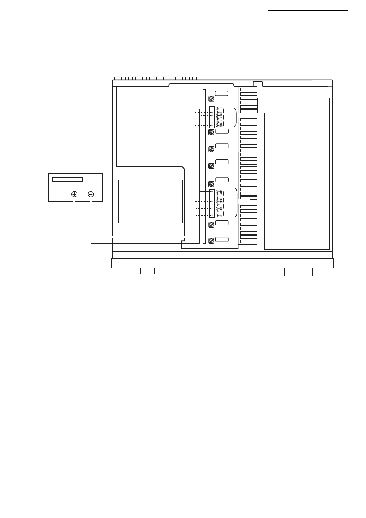
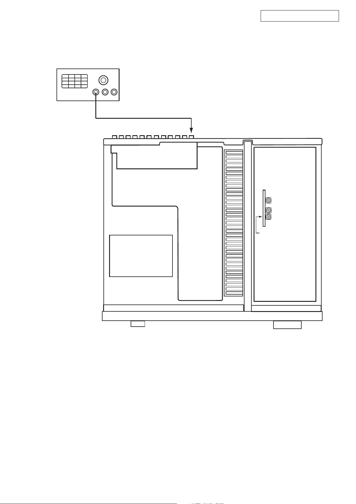
WIRE ARRANGEMENT
If wire bundles are untied or moved to perform adjustment or
parts replacement etc., be sure to rearrange them neatly as
they were originally bundled or placed afterward.
Otherwise, incorrect arrangement can be a cause of noise
generation.
Wire arrangement viewed from the top
ワイヤー整形図
調整や部品の交換等により、ワイヤー類の結束をはずしたり移
動させた場合には、それらの作業が完了した時点でワイヤーの
整形をおこなってください。正しく整形されてないとノイズ発
生の原因となることがあります。
上面からみたワイヤー整形
3

AVR-2805/985/AVC-2890
CAUTION IN SERVICING
Initializing AV SURROUND RECEIVER
AV SURROUND RECEIVER initialization should be performed
when the µcom, peripheral parts of µcom, and Digital P.W.B. are
replaced.
1. Switch off the unit.
2. Hold the following MODE button and ANALOG button, and
switch on the unit.
3. Check that the entire display is flashing with an interval of
about 1 second, and release your fingers from the 2 buttons
and the microprocessor will be initialized.
・If step 3 does not work, start over from step 1.
Note:
・ All user settings will be lost and this factory setting will
be recovered when this initialization mode.
So make sure to memorize your setting for restoring
after the initialization.
サービス時の注意事項
AVサラウンドアンプの初期化について
マイコンやマイコン周辺部品、Digital 基板等を交換した場合
は、AV サラウンドアンプの初期化を行って下さい。
1. オン/オフボタンを OFF にします。
2. MODE ボタンと ANALOG ボタンを同時に押しながら、
オン/オフボタンを押して ON にします。
3. ディスプレイ表示が約 1秒間隔で点滅するのを確認後、2
つのボタンから指を離します。
*マイコンが初期化されます。
注意 :・上記 3 の状態にならない場合は、もう一度操作 1 か
らやり直してください。
・初期化を行うとお客様が設定した内容が工場出荷状
態に戻りますので、あらかじめ設定内容を控えてお
き初期化後再設定してください。
4

AVR-2805/985/AVC-2890
ADJUSTMENT
Audio Section
Idling Current (1U-3469-1)
Required measurement equipment: DC Voltmeter
1. Preparation
(1) Avoid direct blow from an air conditioner or an electric
fan, and adjust the unit at normal room temperature 15 °C
~ 30 °C (59 °F ~ 86 °F).
(2) Presetting
• POWER (Power source switch) OFF
• SPEAKER (Speaker terminal) No load
(Do not connect speaker, dummy resistor, etc.)
2. Adjustment
(1) Remove top cover and set VR101, VR102, VR201,
VR301, VR302, VR401, VR402, on 1U-3469-1 (Power
Unit) at fully counterclockwise ( ).
(2) Connect DC Voltmeter to test points (FRONT-Lch:TP301
① ② pin, FRONT-Rch: TP101 ⑤ ⑥ pin, CENTER ch:
TP301③ ④pin, SURROUND-Lch: TP101③ ④pin, SURROUND-Rch: TP101 ① ② pin, SURROUND BACK-Lch:
TP301 ⑦ ⑧ pin, SURROUND BACK-Rch: TP301 ⑤ ⑥
pin).
(3) Connect power cord to AC Line, and turn power switch
"ON".
(4) Presetting.
MASTER VOLUME : "---" counterclockwise ( min.)
MODE : 7CH STEREO
FUNCTION : CD
(5) Allow 2 minutes, and turn VR101 clockwise ( ) to ad-
just the TEST POINT voltage to 6.5 mV ± 0.5 mV DC.
(6) After 10 minutes from preset, turn VR101 to set the volt-
age to 8 mV ± 0.5 mV DC.
(7) Adjust the Variable Resistors of other channels in the
same way.
(8) After 5 minutes from (6), turn VR101 to set the voltage to
8 m ± 0.5 mV DC.
(9) Adjust the Variable Resistors of other channels in the
same way.
調整
オーディオセクション
アイドリング電流の調整 (1U-3469-1)
調整に必要な測定器 : DCVoltmeter
1. 準備
(1) セットをクーラ、扇風機のそばなど風通しの良い場所
を避け、通常の使用状態に置きます。セットの周囲温
度は 15〜30 ℃、湿度は常湿とします。
(2) プリセット
・電源スイッチ OFF
・スピーカ端子 無負荷
( スピーカ・ダミー抵抗器などを接続しない。)
2. 調整
(1) 上カバーをはずし、1U-3469-1(パワーユニット)の
VR101,VR102,VR201,VR301,VR302,VR401,VR402 を反
時計方向 ( )に回し切った状態にセットします。
(2) テストポイント (FRONT-Lch:TP301 ①② pin,FRONT-
TP101 ⑤⑥ pin,CENTERch:TP301 ③④ pin,
Rch:
SURROUND-Lch:TP101 ③④ pin,SURROUND-Rch:
TP101 ①② pin,SURROUNDBACK-Lch:TP301 ⑦⑧ pin,
SURROUNDBACK-Rch:TP301 ⑤⑥ pin)に DC
Voltmeterを接続します。
(3) 電源コードを AC100V(95〜105Vの範囲でも可)に接
続し、電源スイッチを "ON"にします。
(4) ON後、次のようにセットします。
・MASTERVOLUME(音量調節つまみ)→反時計方向
( )に回す、最小の状態にする。
・SPEAKER(スピーカ端子)→無負荷(スピーカ、
ダミー抵抗器などを接続しない。)
MODE:7CHSTEREO
FUNCTION:CD
(5) 2分以内に VR101を時計方向 ( ) に回しテストポイ
ントの電圧を次のように調整します。
6.5mV ±0.5mVDC
(6) 予備調整から 10分後 VR101を回し、次のように電圧を
設定します。
8mV± 0.5mVDC
(7) 同じ方法で各チャネルの可変抵抗を調整します。
(8) (6) 項設定から 5分後 VR101を回し、次のように電圧を
設定します。
8mV± 0.5mVDC
(9) 同じ方法で各チャネルの可変抵抗を調整します。
5
DC Voltmeter
SR ch
VR302
SL ch
VR301
FR ch
VR102
FL ch
VR101
C ch
VR201
SBR ch
VR402
SR ch
SL ch
FR ch
FL ch
C ch
SBR ch
SBL ch
AVR-2805/985/AVC-2890
TP101
TP301
SBL ch
VR401
Audio Section
6

AVR-2805/985/AVC-2890
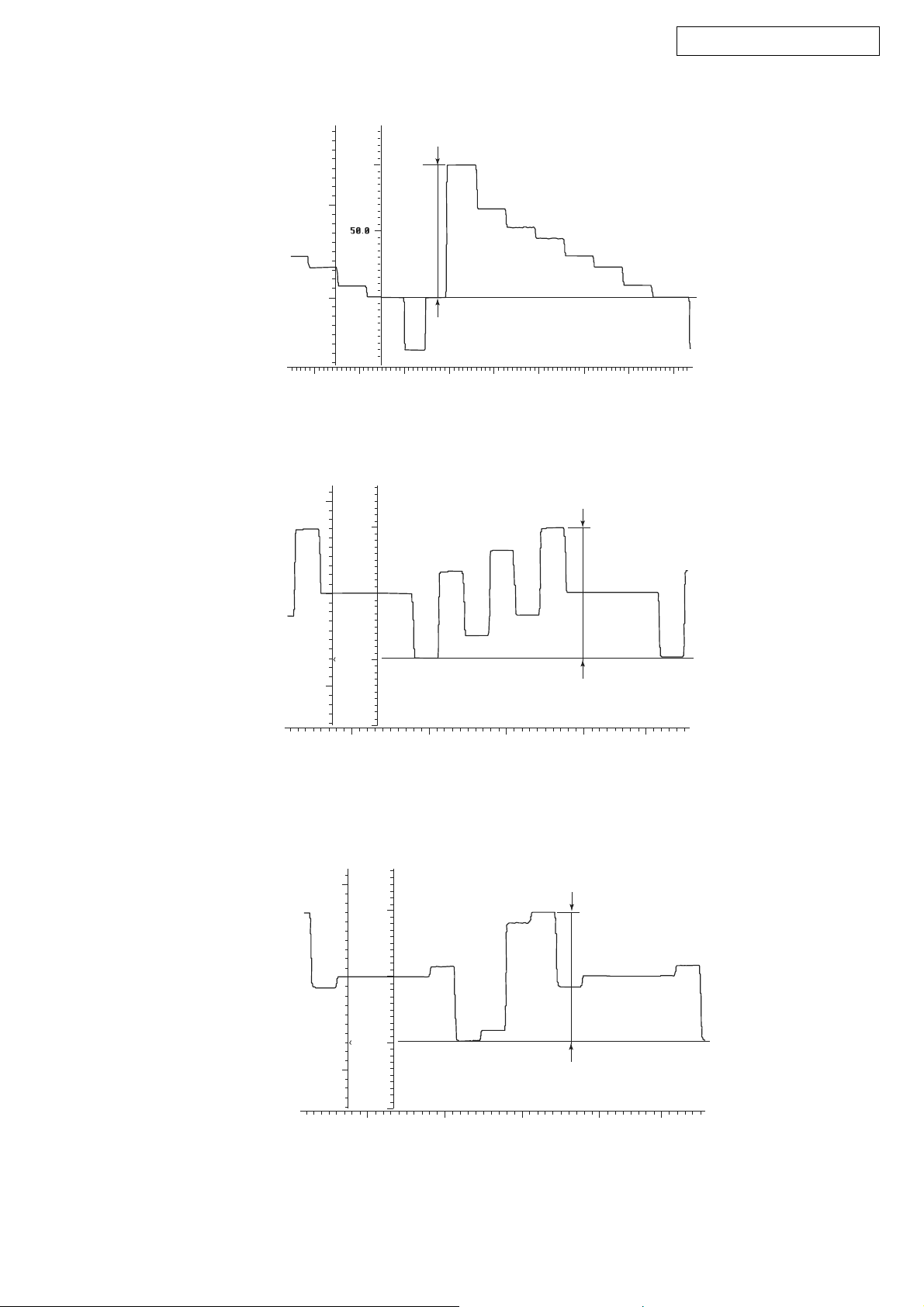
Video Section
Component Video Level Adjustment
Required measurement equipment etc.: Oscilloscope, DVD
VIDEO PLAYER (ex: DVD-1500)
Test disc: DVD T-S01
1. Preparation
(1) Avoid direct blow from an air conditioner or an electric
fan, and adjust the unit at normal room temperature 15 °C
~ 30 °C (59 °F ~ 86 °F).
(2) Playback the color-bar 75% of the Test Disc (Title 12) us-
ing the DVD Video Player, and check that Y and C levels
of the S terminal output are within the specified output
levels.
If they are out of the specified levels, adjust with the variable resister inside of the unit.
(3) Presetting
• POWER (Power source switch) OFF
• SPEAKER (Speaker terminal) No load
(Do not connect speaker, dummy resistor, etc.)
• DVD (Video terminal) No input
2. Adjustment
(1) Remove top cover and set VR101, VR102, VR103, on
1U-3602-1 (Convert Unit) at fully counterclockwise ( ).
(2) Connect a pin-plug terminated with 75-ohms to Y (Cb, Cr)
of the Component Video Monitor Output, and hook up the
Oscilloscope’s probe to both ends of the pin-plug.
(3) Connect S terminal output of the DVD Player with the
DVD input terminal of the Receiver.
(4) Connect power cord to AC Line, and turn power switch
"ON".
(5) Presetting.
• FUNCTION: DVD
• Playback the color-bar 75% of the Test Disc (Title 12)
(6) Turn VR101 clockwise ( ) to adjust the COMPONENT
Video Y voltage (except H. Sync) to 714 ± 50 mVp-p. (Refer to Fig. 1)
(7) Adjust the Variable Resistors of Cb: VR102 and Cr:
VR103 in the same way. (Refer to Fig. 2, 3)
Cb,Cr: 486 ± 50 mVp-p. (U.S.A. & Canada model)
525 ± 50 mVp-p. (Others)
ビデオセクション
コンポーネントビデオレベルの調整
調整に必要な測定器 : Oscilloscope,DVDVIDEOPLAYER
( 例 :DVD-1500)
テストディスク : DVDT-S01
1. 準備
(1) セットをクーラ、扇風機のそばなど風通しの良い場所
を避け、通常の使用状態に置きます。セットの周囲温
度は 15〜30 ℃、湿度は常湿とします。
(2) DVDVIDEOPLAYER でテストディスクのカラーバー
75%(Title12) を再生し、S 端子出力 Y、C レベルが正規
の出力レベルであることを確認する。正規の出力レベ
ルでない場合は、セット内部の可変抵抗器で調整して
ください。
(3) プリセット
・電源スイッチ OFF
・スピーカ端子 無負荷
( スピーカ・ダミー抵抗器などを接続しない。)
・DVD 入力端子 無入力
2. 調整
(1) 上カバーをはずし、1U-3602-1(コンバートユニット)
の VR101,VR102,VR103 を反時計方向 ( )に回し切っ
た状態にセットします。
(2) コンポーネントビデオモニターアウトの Y(Cb,Cr) に
75Ω で終端したピンプラグを接続し、その両端を
Oscilloscope のプローブでつまみます。
(3) DVDVIDEOPLAYER の S 端子出力を本機の DVD 入力端
子に接続します。
(4) 電源コードを電源コンセントに接続し、電源スイッチ
を "ON"にします。
(5) ON後、次のようにセットします。
・本機の FUNCTION を DVD にする。
・テストディスクのカラーバー 75%(Title12) を再生す
る。
(6) VR101を時計方向 ( ) に回しコンポーネントビデオ
Y(H.Sync を除く ) の電圧を調整します。(Fig.1 参照 )
714mV ±50mVp-p
(7) 同じ方法で Cb:VR102、Cr:VR103 の可変抵抗器を調整
します。(fig.2、3 参照 )
Cb,Cr:525± 50mVp-p
7
Oscilloscope
AVR-2805/985/AVC-2890
Video Section
VR103Cr
Cb
VR102
VR101
Component Video Y
8
AVR-2805/985/AVC-2890
Volts
IRE:FLT
100.0
0.5
0.0
0.5
-20.0 -10.0 0.0
Volts
0.5
IRE:FLT
50.0
Y-Signal
714±50mV
p-p
10.0
20.0 30.0
Fig.1 Component Video Y signal
40.0 50.0 60.0
486±50mV (U.S.A. & Canada model)
p-p
525±50mV (Others)
p-p
0.0
-0.5
Volts
0.5
0.0
0.0
-50.0
0.0
IRE:FLT
50.0
0.0
-50.0
20.0
Fig.2 Cb signal
40.0
60.0
486±50mV (U.S.A. & Canada model)
525±50mV (Others)
80.0
p-p
p-p
-0.5
0.0
20.0
Fig.3 Cr signal
9
40.0
60.0
80.0
BLOCK DIAGRAMS (1/2)
AUDIO SECTION
AVR-2805/985/AVC-2890
10
BLOCK DIAGRAMS (2/2)
VIDEO SECTION
AVR-2805/985/AVC-2890
11
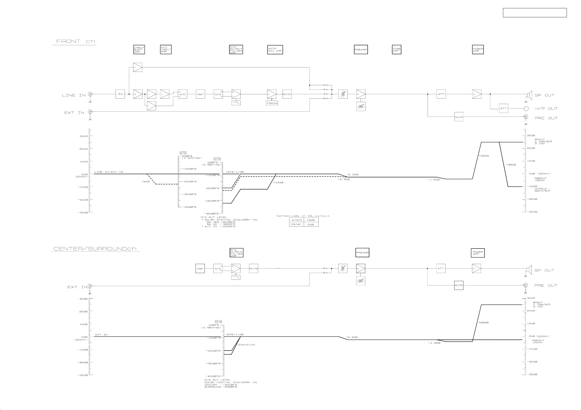
LEVEL DIAGRAMS (1/2)
AVR-2805/985/AVC-2890
12
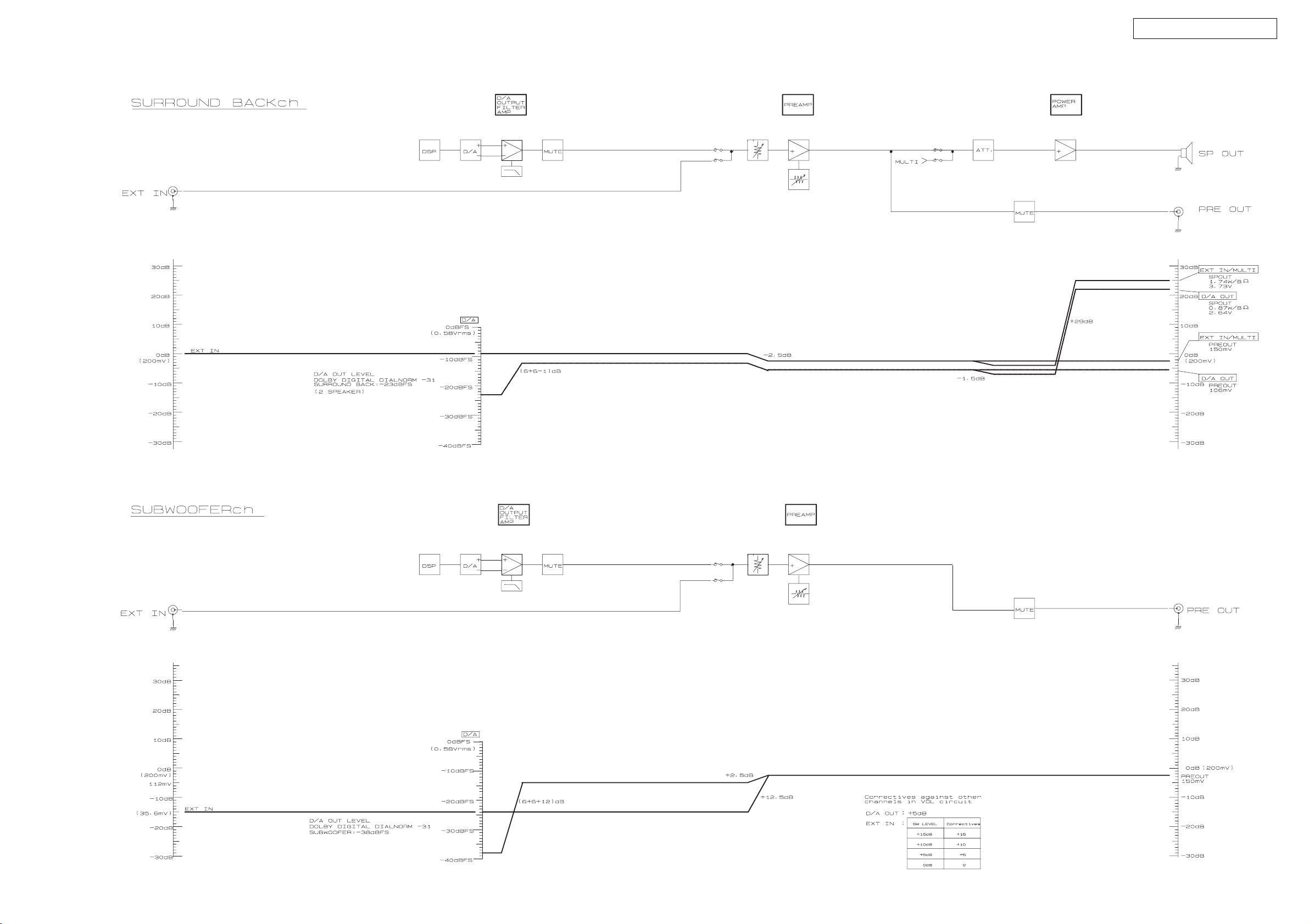
LEVEL DIAGRAMS (2/2)
AVR-2805/985/AVC-2890
13

CLOCK FLOW & WAVE FORM IN DIGITAL BLOCK
Wave form
1
CH1: D-DATA
(IC511 (5) )
INPUT
SELECTOR
AVR-2805/985/AVC-2890
1
DIR
BUFFER
2
DSP
2
CH1: DATA
CH2: fs
CH3: 64fs
3
CH1: DATA
CH2: fs
INPUT
COAXIAL-1
COAXIAL-2
OPTICAL-1
OPTICAL-2
OPTICAL-3
OPTICAL-4
OPTICAL-5
OUTPUT
OPTICAL-3
OPTICAL-4
IC511
SN74HC
151APW
(3)
(2)
(12) (5)
(13)
(14)
(15)
(1)
OUTPUT
SELECTOR
IC512
SN74HC
151APW
(3)
(2)
(12)
(13) (5)
(14)
(15)
(1)
IC513
LC89057W
RDATA (21)
SLRCK (23)
(4) RX2
SBCK (22)
RMCK (16)
RBCK (17)
RLRCK (20)
ADIN (24)
12.288MHz
IC514
FCX0-03
(3)
(29) XIN
DATA
fs
64fs
256fs
64fs
fs
IC515
SN74LV
244APW
(2)- -(18)
(13)- -(7)
(11)- -(9)
(15)- -(5)
(17)- -(3)
(4)- -(16)
(6)- -(14)
(8)- -(12)
2
IC906
ADSP-21266
(94) DAI_P20
(78) DAI_P11
(79) DAI_P12
(71) DAI_P9
(77) DAI_P10
DAI_P16 (86)
DAI_P15 (82)
DAI_P14 (81)
DAI_P13 (80)
CODEC
IC611
AD1835
I²SMODE
DSDATA1 (41)
DSDATA2 (42)
DSDATA3 (43)
DSDATA4 (44)
(38) DBCLK
(37) DLRCK
(47) MCLK
(46) ALRCK
(45) ABCLK
(49) ASDATA
Selector
IC610
74LVX
157MTC
(02) (03)
(04)
(05) (06)
(07)
(11) (10)
(09)
(14) (13)
(12)
3
GND
CH3: 64fs
CH4: 256fs
3
14
AVR-2805/985/AVC-2890
CHECK WITH TEST MODE
µcom/DSP Error Display Mode
1. Operation Spec
µcom version display mode:
When the following conditions are satisfied at its starting state, error information is displayed before version information.
Starting method (same as µcom version display):
While pressing 2 buttons, "DIMMER (S11)" and "STATUS (S14)", plug the AC cord to the wall outlet.
Then, press "STATUS" button to display the following information on the FL Display.
2. Display Order
Error information →Main-µcom version information → Sub-µcom version information → DSP version information
3. Display
Any one of the following list is displayed, in the priority of ①②③④ .
Condition State Display
①
Sub-µcom NG
②
DIR NG
③
DSP NG
④
Both SUB/DSP OK
No response from Sub-µcom
No response from DIR
When DSP boot, executing DSP reset
makes no change to BUSY port "L".
No change to BUSY port "L" before issuing DSP command.
When DSP data read, executing WRITE="L"
makes no change to ACK="H".
When DSP data read, executing REQ="L"
makes no change to ACK="L".
When DSP data write, executing WRITE="H"
makes no change to ACK="H".
When DSP data write, executing REQ="L"
makes no change to ACK="L".
When DSP special code boot, executing DSP reset
makes no change to BUSY port "L".
No change to BUSY port "L" before issuing
DSP special read command.
No change to BUSY port "L" before DSP version read.
" □ SUB □□ ERROR □01□ "
" □ DIR □□ ERROR □01□ "
" □ DSP □ ERROR □01□ "
" □ DSP □ ERROR □02□ "
" □ DSP □ ERROR □03□ "
" □ DSP □ ERROR □04□ "
" □ DSP □ ERROR □05□ "
" □ DSP □ ERROR □06□ "
" □ DSP □ ERROR □11□ "
" □ DSP □ ERROR □12□ "
" □ DSP □ ERROR □13□ "
(No error display, version display only)
テストモードによるチェック方法
マイコン・DSP エラー表示モード
1. 動作仕様
マイコンバージョン表示モード :
起動状態にて下記の条件に該当した場合は、バージョン情報表示の前にエラー情報を表示します。
起動方法 ( マイコンバージョン表示と同様 ):
"DIMMER"(S11),"STATUS"(S14) の 2 つのボタンを押した状態で、AC コードを差し込みます。
その後、STATUS ボタンを押すと下表の内容が FLDisplay に表示されます。
2. 表示順序
エラー情報→メインマイコンバージョン情報→サブマイコンバージョン情報→DSP バージョン情報
3. 表示条件
下表のいずれかを表示します。表示の優先順は、①②③④。
条件 状態 表示内容
① SUB マイコンが NG SUB マイコンからの応答がない " □ SUB □□ ERROR □01□ "
② DIR が NG DIR からの応答がない " □ DIR □□ ERROR □01□ "
③ DSP が NG DSP コードブート時、DSP リセットを実行しても
BUSY ポートが "L" にならない
DSP コマンド発行前に、BUSY ポートが "L" にならない " □ DSP □ ERROR □02□ "
DSP データリード時、WRITE="L" としても ACK="H" とならない " □ DSP □ ERROR □03□ "
DSP データリード時、REQ="L" としても ACK="L" とならない " □ DSP □ ERROR □04□ "
DSP データライト時、WRITE="H" としても ACK="H" とならない " □ DSP □ ERROR □05□ "
DSP データライト時、REQ="L" としても ACK="L" とにならない " □ DSP □ ERROR □06□ "
DSP スペシャルコードブート時、DSP リセットを実行しても
BUSY ポートが "L" にならない
DSP スペシャルリードコマンド発行前に、
BUSY ポートが "L" にならない
DSP バージョンリード前に、BUSY ポートが "L" にならない " □ DSP □ ERROR □13□ "
④SUB/DSP共にOK
" □ DSP □ ERROR □01□ "
" □ DSP □ ERROR □11□ "
" □ DSP □ ERROR □12□ "
( 表示せずにバージョン表示を行う )
15
SEMICONDUCTORS
Only major semiconductors are shown, general semiconductors etc. are omitted to list.
主な半導体を記載しています。汎用の半導体は記載を省略しています。
1. IC’s
Note : Abbreviation ahead of IC No. indicates the name of P.W.B., etc.
注 ): ICNo. の前の記号は、基板の名称を表します。
PO : Power P.W.B. AC : Amp Connect P.W.B.
CV : Connect/Video P.W.B. AD : Audio/Digital P.W.B.
CO : Control P.W.B. VI : Video Convert P.W.B.
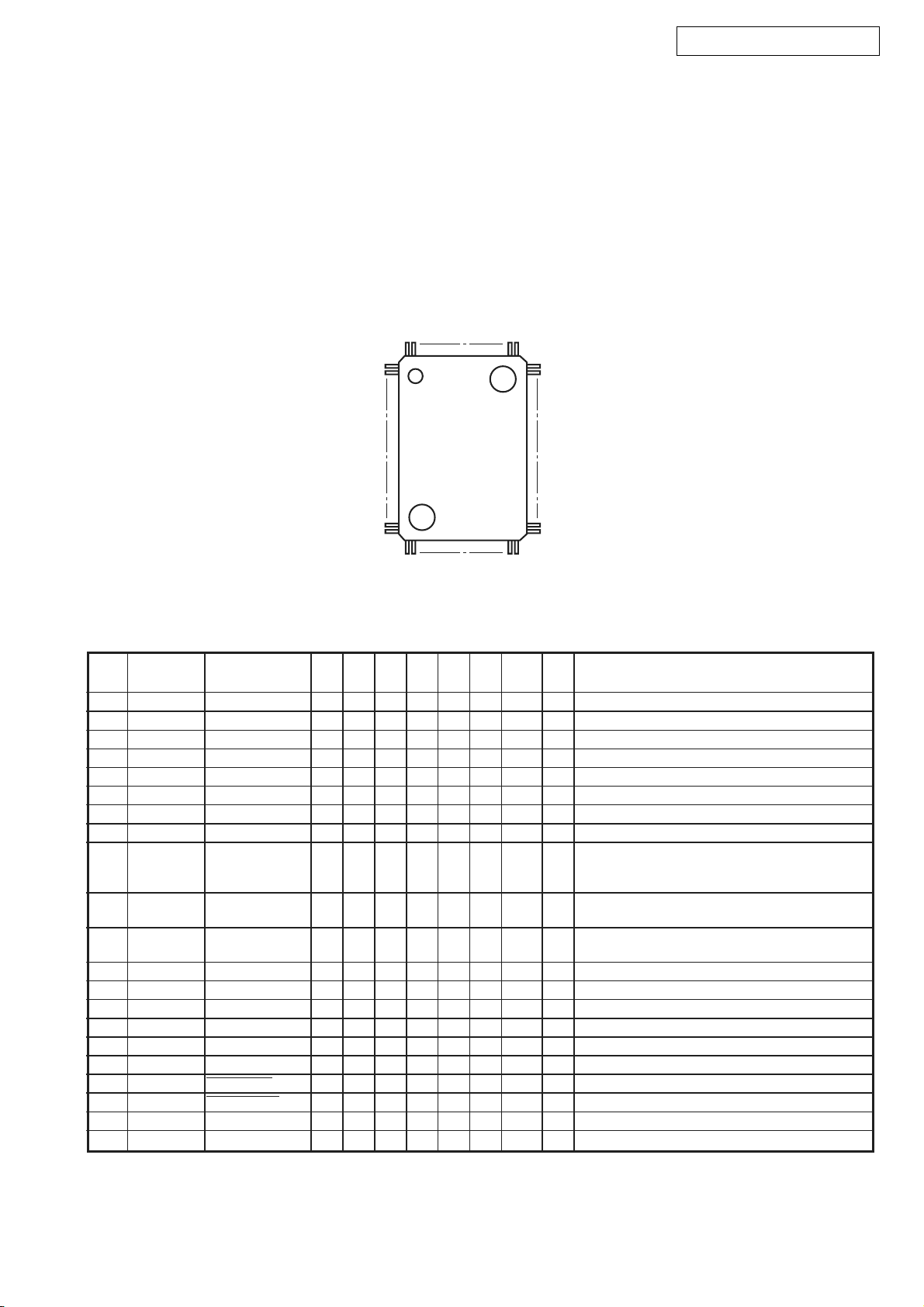
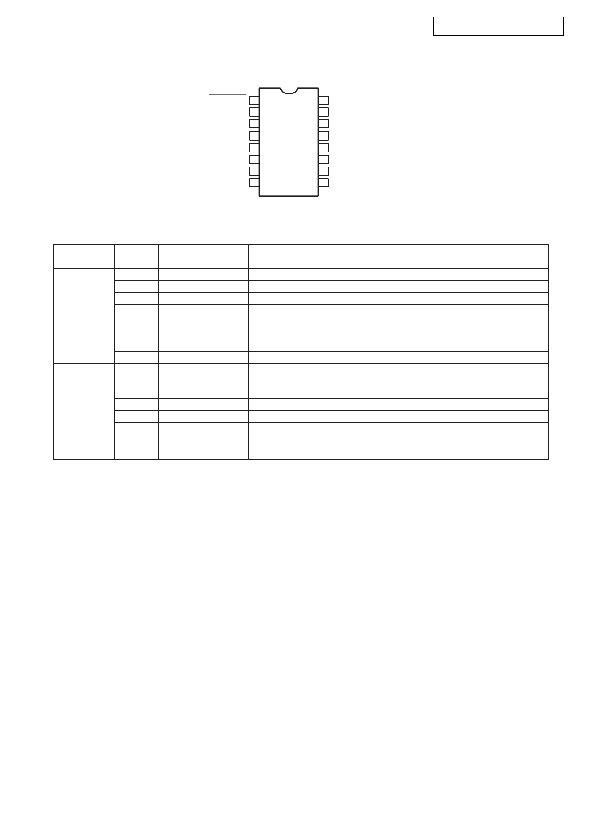
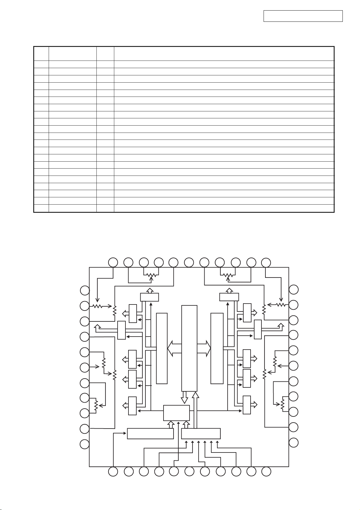
M30624MGAFP (CO: IC506)
100 81
AVR-2805/985/AVC-2890
1
TOP VIEW
30
31 50
80
51
M30624MGAFP Terminal Function
Pin
Pin Name FunctionI/O
No.
1 P96/SOUT4 PLRDS DATA O C Z O/L O/L PLL & RDS control pin (LC72131 & LC72722)
2 P95/CLK4 PLRDS CLK O C Z O/L O/L PLL & RDS control pin (LC72131 & LC72722)
3 P94/TB4 PLL STB O C Z O/L O/L PLL control pin (LC72131)
4 P93/TB3 OSD RST O C Z O/L O/L OSD control pin (M35015)
5 P92/SOUT3 OSD DATA O C Z O/L O/L OSD control pin (M35015)
6 P91/SIN3 OSD STB O C Z O/L O/L OSD control pin (M35015)
7 P90/CLK3 OSD CLK O C Z O/L O/L OSD control pin (M35015)
8 BYTE BYTE GND (Ext. data bus bit width switching, 16bit: L)
9 CNVCS CNVSS
10 P87 ISEL B I Lv Eu Z O/L O/L
11 P86 ISEL A I Lv Eu Z O/L O/L
12 RESET _RESET I Lv Eu L I I Reset input
13 XOUT X1 O Oscillator connection
14 VSS VSS GND
15 XIN X2 I I I Oscillator connection
16 VCC VCC +5V
17 P85/NMI _NMI I Not used (Fixed to H)
18 P84/INT2 _B. DOWN I
19 P83/INT1 _PROTECT I
20 P82/INT0 REMOCON I
21 P81 VSEL A I Lv Eu Z I O/L Master VR rotation detect input (Rotary encoder)
Symbol
Type
Op
Op
Det
(Int.)
E↓&L
Eu Z I I Power down detect (Power down: L)
E↓&L
Ed Z I I Protection detect input (Detected: L)
E↑&L
Z I I Remote control signal input
Re s STBY Stop
(Ext.)
Single-chip/Micro-processor mode switching
(Normal single-chip: L, Rewrite boot program start:
H input set)
Input selector rotation detect input
(Rotary encoder)
Input selector rotation detect input
(Rotary encoder)
16
AVR-2805/985/AVC-2890
Op
(Int.)
Op
Re s STBY Stop
(Ext.)
STB output for function switching control
(L-ch INPUT&REC/ZONE, EXT. IN)
STB output for function switching control
(R-ch INPUT&REC/ZONE)
CLK output for video switching expander control
(BU4094B)
DATA output for video switching expander control
(BU4094B)
OE output for video switching expander control
(BU4094B)
STB output for video switching expander control
(BU4094B)
CENTER PREOUT output muting control,
L: Muting
SURROUND PREOUT output muting control,
L: Muting
SURROUND BACK PREOUT output muting
control, L: Muting
SUB WOOFER PREOUT output muting control,
L: Muting
SURROUND BACK POWER AMP input muting
control, L: Muting
Pin
Pin Name FunctionI/O
No.
22 P80 VSEL B I Lv Eu Z O/L O/L Master VR rotation detect input (Rotary encoder)
23 P77 FUNC STB1 O C Z O/L O/L
24 P76 FUNC CLK O C Z O/L O/L CLK output for function switching control
25 P75 FUNC DATA O C - Z O/L O/L DATA output for function switching control
26 P74 FUNC STB2 O C Z O/L O/L
27 P73/CTS2 FL DATA O C Z O/L O/L FL tube control pin (LC75721E)
28 P72/CLK2 FL CLK O C Z O/L O/L FL tube control pin (LC75721E)
29 P71/RXD2 H/P DET I Z O/L O/L H/P detect input (Detected: H)
30 P70/TXD2 TUNER POWER O N Eu Z O/L O/L TUNER power on/off switching (H: ON)
31 P67/TXD1 TxD O C Z O/L O/L Data transfer pin to outside
32 P66/RXD1 RxD I Lv Z I I Data receive pin from outside
33 P65/CLK1 RESET2 O C Ed Z O/L O/L SUB-µcom reset output
34 P64/CTS1 ACK O C Ed Z O/L O/L MAIN-SUB µcom comm. control pin
35 P63/TXD0 MOSI O C Ed Z O/L O/L MAIN-SUB µcom comm. control pin
36 P62/RXD0 MISO I Lv Ed Z I I MAIN-SUB µcom comm. control pin
37 P61/CLK0 TRIGGER SW 2 OC Z O/L O/L TRIGGER SW 2 control pin
38 P60/CTS0 E.VOL STB O C Z O/L O/L E-VR control output (TC94A27)
39 P57 E.VOL CLK O C Z O/L O/L E-VR control output (TC94A27, TC9459)
40 P56 E.VOL DATA O C Z O/L O/L E-VR control output (TC94A27, TC9459)
41 P55/EPM FRASH EPM I Lv Z I I Rewrite boot program start: L input set
42 P54 VSDA I/O C Z I O/L VIDEO IC (Chroma decoder, 3D Y/C) control pin
43 P53 VSCL I/O C Z I O/L VIDEO IC (Chroma decoder, 3D Y/C) control pin
44 P52 FL RST O C Ed Z O/L O/L FL tube control pin (LC75721E)
45 P51 FL CE1 OC Z O/L O/L FL tube control pin (LC75721E)
46 P50/CE FRASH CE I Z I I Rewrite boot program start: H input set
47 P47 V.EXP CLK O C Z O/L O/L
48 P46 V.EXP DATA O C Z O/L O/L
49 P45 V.EXP OE O C Ed Z O/L O/L
50 P44 V.EXP STB O C Z O/L O/L
51 P43 H/P RELAY O C Z O/L O/L H/P relay control (H: ON)
52 P42 S BACK RELAY O C Z O/L O/L Relay control for SURROUND BACK SP
53 P41 SA-RELAY O C Z O/L O/L Relay control for FRONT A SP
54 P40 SB-RELAY O C Z O/L O/L Relay control for FRONT B SP
55 P37 C-RELAY O C Z O/L O/L Relay control for CENTER SP
56 P36 F-RELAY O C Z O/L O/L Relay control for SURROUND SP
57 P35 PRE F MUTE O C Z O/L O/L FRONT PREOUT output muting control, L: Muting
58 P34 PRE C MUTE O C Z O/L O/L
59 P33 PRE S MUTE O C Z O/L O/L
60 P32 PRE SB MUTE O C Z O/L O/L
61 P31
62 VCC VCC +5V
63 P30 MULTI MUTE O C Z O/L O/L Pin-jack output muting control of MULTI, L: Muting
64 VSS VSS GND
65 P27 VOL MUTE O C Z O/L O/L POWER AMP input muting control, L: Muting
66 P26
67 P25 TUNER MUTE O C Z O/L O/L TUNER muting control
Symbol
SUB WOOFER MUTE
S.BACK VOL MUTE
OC Z O/L O/L
OC Z O/L O/L
Type
Det
17
AVR-2805/985/AVC-2890
Op
Pin
Pin Name FunctionI/O
No.
68 P24 GRN LED OC Z O/L O/L LED control pin
69 P23 FL CE2 OC Z O/L O/L FL tube control pin (LC75721E)
70 P22 S MONI. DET I Lv Eu Z O/L O/L S-monitor connection detect input (L: Connected)
71 P21 S SIG. DET I Lv Eu Z O/L O/L S-signal detect input (H: S-signal inputted)
72 P20 SYNC. DET I Lv Eu Z I I Sync. detect input (H: Ext. synchronized)
73 P17/INT5 RDS DATAOUT I
74 P16/INT4 REQ I
75 P15/INT3 POWER KEY I
76 P14/D12 RSPOWER O C Ed Z O/H O/L
77 P13/D11 RECINHA O C Z O/L O/L
78 P12/D10 SSEL B I C Z I O/L
79 P11/D9 SSEL A I C Z I O/L
80 P10/D8 A+B LIMIT O C Z O/L O/L
81 P07/D7 VSIGDET I Z O/L O/L VIDEO signal detect port
82 P06/D6 COMPSIGDET I Z O/L O/L COMPONENT signal detect port
83 P05/D5 VIDEO POWER O C Z O/L O/L VIDEO power on/off switching (H: ON)
Symbol
Type
Det
E↓&L
E↓&L
E↓&L
Op
Re s STBY Stop
(Ext.)
(Int.)
I O/L RDS data input (LC72722)
Ed Z I I MAIN-SUB µcom comm. control pin
I O/L Interrupt port for WAIT mode cancel
Same logic as POWER port,
when STANDBY mode: H
When RECOUT select is VCR1 or VIDEO other
than VCR system: H
Select encoder rotation detect input (Rotary
encoder)
Select encoder rotation detect input (Rotary
encoder)
FRONT AMP current limiter control, when
FRONT SP A+B: H
84 P04/D4 TRIGER SW 1 OC Z O/L O/L
85 P03/D3 MIC ON OC Z O/L O/L MIC input used: H, Other: L
86 P02/D2 RECINHB O C Z O/L O/L When RECOUT select is VCR1 or VCR2: H
87 P01/D1 POWER O C Ed Z O/L O/L Power relay control output (H: ON)
88 P00/D0 RED LED OCEu Z O/L O/L LED control pin
89 P107/AN7 KEY1 I Lv Eu Z O/L O/L Button input 1
90 P106/AN6 KEY2 I Lv Eu Z O/L O/L Button input 2
91 P105/AN5 KEY3 I Lv Eu Z O/L O/L Button input 3
92 P104/AN4 STEREO I Lv Eu Z O/L O/L When TUNER FM stereo receive: L
93 P103/AN3 TUNED I Lv Eu Z O/L O/L TUNER tuned detect (L: Tuned)
94 P102/AN2 RDS CE O C Z O/L O/L RDS data output (LC72722)
95 P101/AN1 RDS RESET O C Z O/L O/L RDS reset output (LC72722)
96 AVSS AVSS AD GND
97 P100/AN0 MODE I Lv Z O/L O/L Destination switching input
98 VREF VREF AD ref. +5V
99 AVCC AVCC AD +5V
100 P97/SIN4 PLL DATAOUT I Lv Z I O/L PLL serial data input pin (LC72131)
TRIGGER SW 1 cotrol pin
18
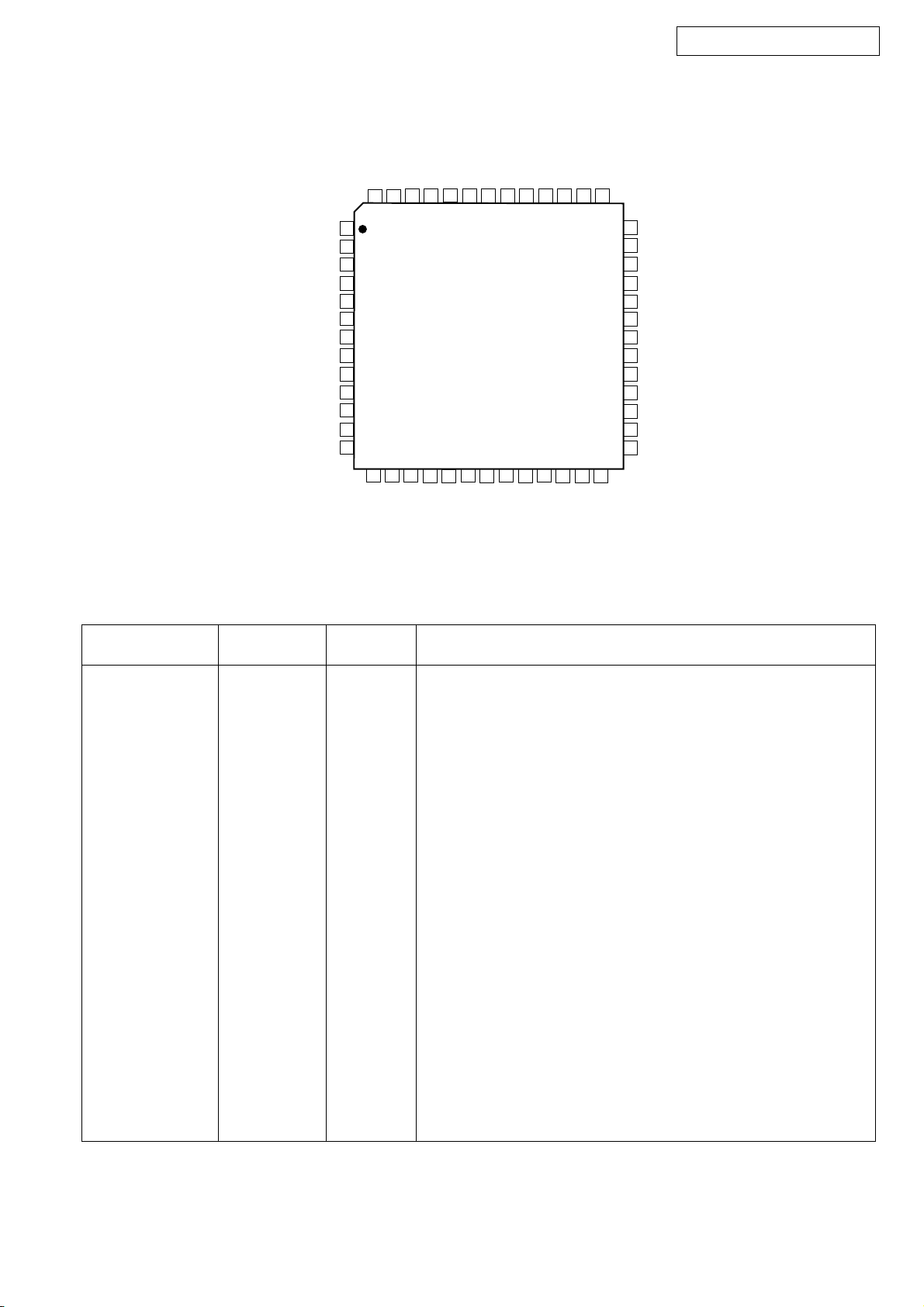
M30622M8P (AD: IC517)
AVR-2805/985/AVC-2890
75
76
100
1
51
50
26
25
M30622M8P Terminal Function
Pin
Pin Name Symbol I/O Type Det
No.
1 P94/TB4 DSP MS O C - - Eu Z DSP control pin
2 P93/TB3 CLATCH O C - - - Z CODEC control pin (AD1835: Chip select)
3 P92/SOUT3 CDATAIN O C - - - Z CODEC control pin (AD1835)
4 P91/SIN3 CODEC_DATAOUT I - - - Eu Z CODEC control pin (AD1835)
5 P90/CLK3 CODEC_CLK O C - - - Z CODEC control pin (AD1835)
6 BYTE BYTE - - - - - - GND (Ext. data bus bit width switching, 16bit: L)
7 CNVCS CNVSS - - - - - -
8 P87 DAC-RESET O C - - - Z
9 P86 NC O C - - - Z NC
10 RESET RESET I - - - - L Reset input (Reset: L)
11 XOUT X1 O - - - - - Oscillator connection
12 VSS VSS - - - - - - GND
13 XIN X2 I - - - - - Oscillator connection
14 VCC VCC - - - - - - +5V
15 P85/NMI _NMI I - - - - - Not used (Fixed to H)
16 P84/INT2 INT1 I -
17 P83/INT1 ACK I -
18 P82/INT0 B.DOWN I - Lv - Eu Z Power down detect (Power down: L)
19 P81 NC O C - - - Z NC
20 P80 NC O C - - - Z NC
21 P77 DIGITAL POWER O C - - Ed Z DIGITAL power on/off switching (H: ON)
22 P76 FGAIN O C - - Ed Z
23 P75 NC O C - - - Z NC
24 P74 NC O C - - - Z NC
25 P73/CTS2 NC O C - - - Z NC
26 P72/CLK2 NC O C - - - Z NC
27 P71/RXD2 VPP I C - - - - Normal: H, Writing flash ROM for DSP: L
28 P70/TXD2 NC O C - - - Z NC
29 P67/TXD1 TxD O C - - Ed Z Data transfer output to outside
E ↓L
E ↓L
Op
(Int.)Op(Ext.)
- Eu Z DIR control pin (LC89057W-E)
-EdZ
Res Function
Single-chip/ Micro-processor mode switching (Normal
single-chip: L, Rewirte boot program start: H input set)
CODEC control pin ("L": Power Down mode,
" ↑ (rising edge)": Reset, "H": Normal)
MAIN/SUB-µcom comm. control input
(ACK from MAIN µcom L retum)
IV AMP GAIN switching control output
(Subwoofer YES: L)
19
AVR-2805/985/AVC-2890
Pin
Pin Name Symbol I/O Type Det
No.
30 P66/RXD1 RxD I - Lv - Ed Z Data receive input from outside
31 P65/CLK1 NC O C - - - Z NC
32 P64/CTS1 REQ O C - - Ed Z
33 P63/TXD0 MISO O C - - Ed Z MAIN/SUB-µcom comm. control terminal (Data output)
34 P62/RXD0 MOSI I - - - Ed Z MAIN/SUB-µcom comm. control terminal (Data input)
35 P61/CLK0 DIR CLK O C - - - Z DIR control pin (LC89057W-E), control clock output
36 P60/CTS0 DIR DIN O C - - Eu Z DIR control pin (LC89057W-E), control data output
37 P57 DIR DOUT I - - - Eu Z DIR control input pin (LC89057W-E), control data input
38 P56 NC O C - - - Z NC
39 P55/EPM FLASH EPM I - Lv - - Z Rewirte boot start: L
40 P54 X'TALRST O C - - - H(Iu) Clock for DIR (L: Osc. Stop)
41 P53 DIR CE O C - - - H(Iu) DIR control pin (LC89057W-E), chip enable output
42 P52 DIR_RST O C - - Ed H(Iu) DIR control output (LC89057W-E), Reset: L
43 P51 NC O C - - - Z NC
44 P50/CE FLASH CE I - - - - Z Rewirte boot program start: H input set
45 P47 NC O C - - - Z NC
46 P46 NC O C - - - Z NC
47 P45 NC O C - - - Z NC
48 P44 NC O C - - - Z NC
49 P43 NC O C - - - Z NC
50 P42 NC O C - - - Z NC
51 P41 NC O C - - - Z NC
52 P40 NC O C - - - Z NC
53 P37 DINA O C - - - Z Digital input switching
54 P36 DINB O C - - - Z Digital input switching
55 P35 DINC O C - - - Z Digital input switching
56 P34 DRECA O C - - - Z Digital RECOUT switching
57 P33 DRECB O C - - - Z Digital RECOUT switching
58 P32 DRECC O C - - - Z Digital RECOUT switching
59 P31 NC O C - - - Z NC
60 VCC VCC - - - - - - +5V
61 P30 NC O C - - - Z NC
62 VSS VSS - - - - - - GND
63 P27 NC O C - - - Z NC
64 P26 (I/O7 SBR) O C - - - Z DSP comm. Terminal
65 P25 (I/O6 SBL) O C - - - Z DSP comm. Terminal
66 P24 NC O C - - - Z NC
67 P23 NC O C - - - Z NC
68 P22 NC O C - - - Z NC
69 P21 NC O C - - - Z NC
70 P20 NC O C - - - Z NC
71 P17/INT5 NC O C - - - Z NC
72 P16/INT4 NC O C - - - Z NC
73 P15/INT3 NC O C - - - Z NC
74 P14/D12 NC O C - - - Z NC
75 P13/D11 NC O C - - - Z NC
76 P12/D10 NC O C - - - Z NC
77 P11/D9 NC O C - - - Z NC
78 P10/D8 NC O C - - - Z NC
79 P07/D7 ROM_RST1 O C - - Ed Z Memory reset for DSP (reset: L)
80 P06/D6 DSP1_RS O C - - - Z DSP reset output pin (reset: L)
81 P05/D5 DSP I/0 POWER O C - - Eu Z
82 P04/D4 DSP OSC ON O C - - - Z ON="L" (After 20ms from DIGITAL POWER ON)
83 P03/D3 NC O C - - - Z NC
84 P02/D2 FLAG 0A I - - - Ed Z E2PROM chip select control for DSP
Op
(Int.)Op(Ext.)
Res Function
MAIN/SUB-µcom comm. control output
(RTS from SUB-µcom L)
POWER ON="L" (After 10ms from DIGITAL POWER ON)
20
AVR-2805/985/AVC-2890
Pin
Pin Name Symbol I/O Type Det
No.
85 P01/D1 FLAG 1A I - Lv - Eu Z Not used
86 P00/D0 FLAG 2A(BUSY1) I - Lv - Eu Z DSP operation check flag (FLAG 2A) Normal="L"
87 P107/AN7 FLAG 3A I - Lv - Eu Z
88 P106/AN6 SELCLK1 O C - - - Z
89 P105/AN5 u ERR MUTE O C - - - Z Mute control for pop noise prevention (Mute="L")
90 P104/AN4 u BSE(AC3 MUTE) O C - - - Z Digital mute control (AC-3 or DTS decode enable: L)
91 P103/AN3 NC O C - - - Z NC
92 P102/AN2 BUSYEPROM O C - - - Z DSP control pin
93 P101/AN1 DSP_BOOT I - - - Eu H(Iu) DSP rewrite boot program (DSP rewrite: L input)
94 AVSS AVSS - - - - - - AD GND
95 P100/AN0 NC O C - - - Z NC
96 VREF VREF - - - - - - AD ref. +3.3V
97 AV CC AVC C - - - - - - A D +3. 3 V
98 P97/SIN4 DSP MISO I - - - Eu Z DSP control pin
99 P96/SOUT4 DSP MOSI O C - - Eu Z DSP control pin
100 P95/CLK4 DSP CLK O C - - - Z DSP control pin
Note: Pin No. : Terminal number of microcomputer.
Port Name : The name entered in the data sheet of microcomputer.
Symbol : Symbolized interface function.
I/O : Input or out of part.
Type : Composition of port in case of output port.
Op : Pull up/Pull down selection information.
Det : Indicates judging state of input port. Level detection is “LV”; Edge detection is “Ed”; Detection by both shifting is “E&L”;
Serial data detection is “S” (Serial data output is also “S”).
Res : State at reset.
STBY : State of port when STANDBY mode.
Stop : State of port when Stop mode.
“I” = Input port
“O” = Output port
“C” = CMOS output
“N” = NMOS open drain output
“P” = PMOS open drain output
“Iu” = Inner microcomputer pull up
“Id” = Inner microcomputer pull down
“Eu” = External microcomputer pull up
“Ed” = External microcomputer pull down
“H” = Outputs High Level at reset
“L” = Outputs Low Level at reset
“Z” = Becomes High impedance mode at reset
“O/L” = Output port and “L”
“I” = Input port
“O/L” = Output port and “L”
“I” = Input port
Op
(Int.)Op(Ext.)
Res Function
Special Flag for ROM update (DSP: FLAG 3A)
ADC/DIR data, clock switching control terminal
(ADC,PCM 1/4 sampling: L) (PCM ・ DD ・ DTS: H)
21
BU4094BCF (VI: IC120), (CO: IC503)
STROBE 1
DATA
CLOCK
BU4094BCF Terminal Function
V
Q1
Q2
Q3
Q4
SS
AVR-2805/985/AVC-2890
V
16
DD
2
3
4
5
6
7
8
15
14
13
12
11
10
OE
Q5
Q6
Q7
Q8
Q’
S
9
Q
S
IC503
IC120
Por t
EXP1 A(RECA) Video input switching (RECOUT SELECT)
EXP2 B(RECB) Video input switching (RECOUT SELECT)
EXP3 C(RECC) Video input switching (RECOUT SELECT)
EXP4 D(INA) Video output switching (INPUT SELECT)
EXP5 E(INB) Video output switching (INPUT SELECT)
EXP6 F(INC) Video output switching (INPUT SELECT)
EXP7 S1 Video output switching
EXP8 S2 Video output switching
EXP9 VIN1 Component video output switching
EXP10 VIN2 Component video output switching
EXP11 VIN3 Component video output switching
EXP12 VINUP Switching control pin of component monitor output
EXP13 Y/C SELA Video output switching
EXP14 SMUTE Video output switching
EXP15 VMONISELA Video output switching
EXP16 VMONISELB Video output switching
Symbol
Function
22
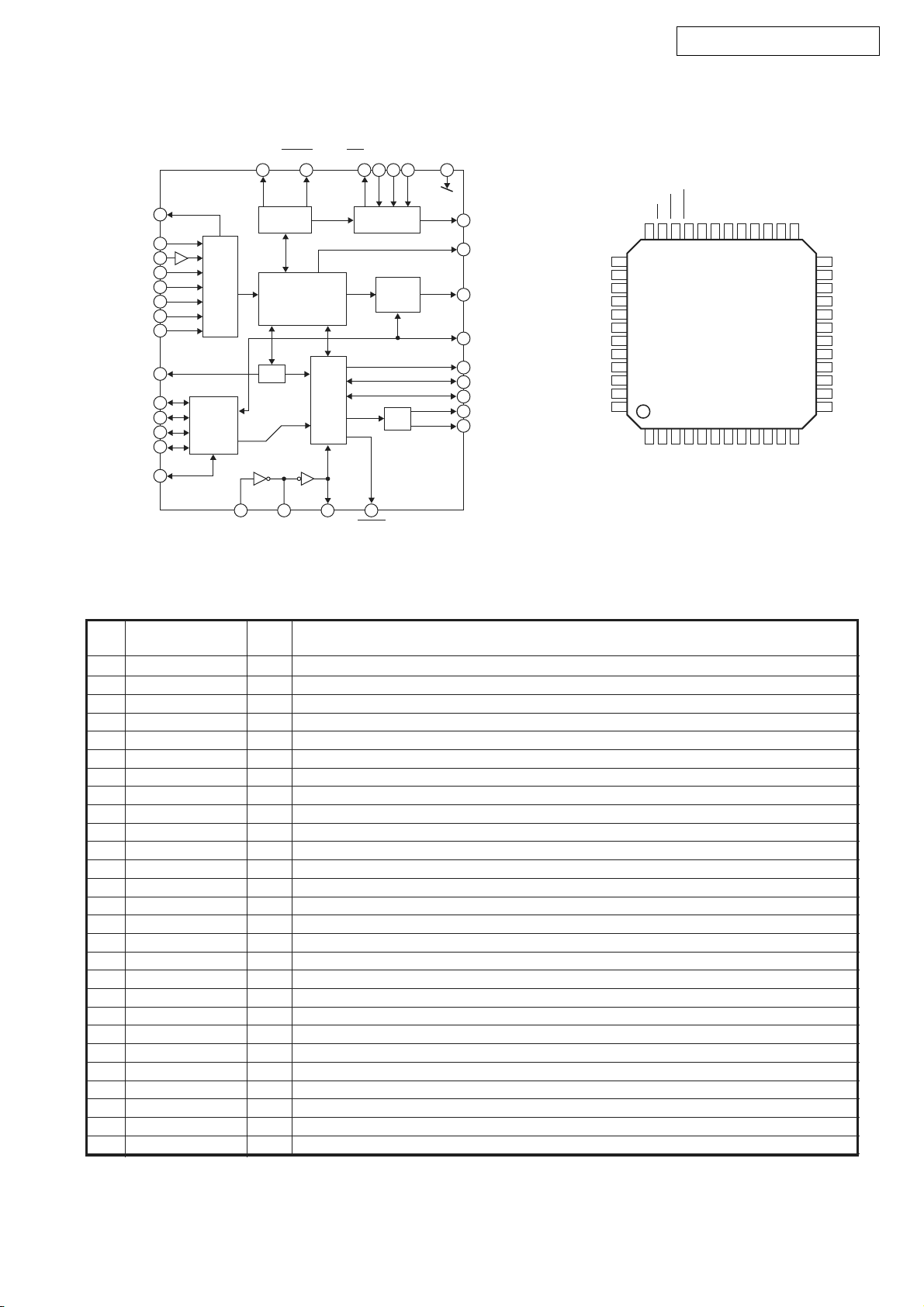
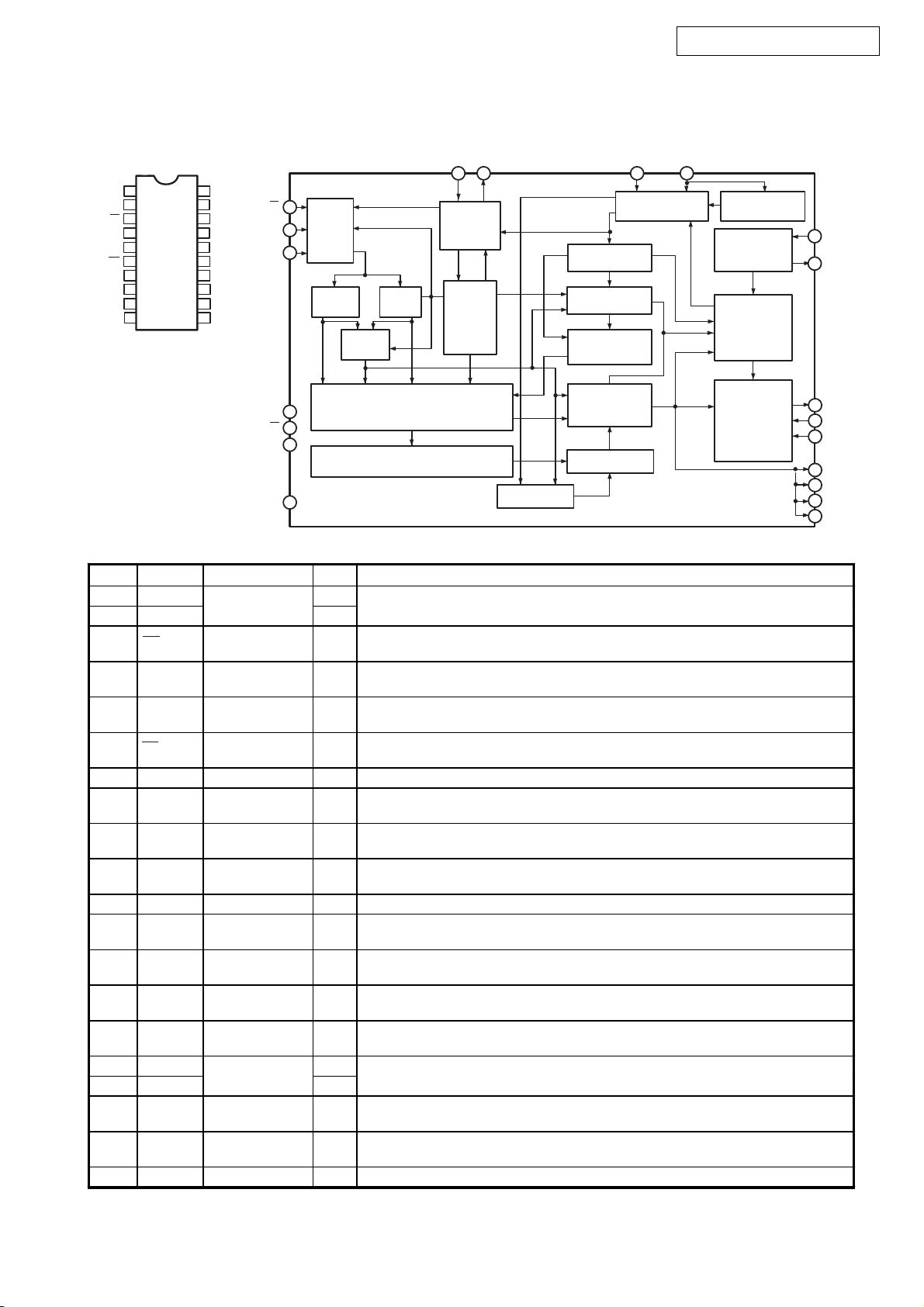
ADSP-21266SKSTZ-2B (AD: IC906)
AVR-2805/985/AVC-2890
144
1
PIN 1 INDICATOR
109
108
TOP VIEW
36
37
73
72
ADSP-21266SKSTZ-2B Terminal Function
LQFP
Pin Name
V
DDINT
Pin # Pin Name
1V
DDINT
CLKCFG0 2 GND 38 GND 74 V
CLKCFG1 3 RD 39 V
BOOTCFG0 4 ALE 40 GND 76 V
LQFP
Pin # Pin Name
37 V
DDEXT
DDINT
LQFP
Pin # Pin Name
73 GND 109
DDINT
75 GND 111
DDINT
BOOTCFG1 5 AD15 41 DAI_P10 (SD2B) 77 GND 113
GND 6 AD14 42 DAI_P11 (SD3A) 78 V
V
DDEXT
7 AD13 43 DAI_P12 (SD3B) 79 GND 115
GND 8 GND 44 DAI_P13 (SCLK23) 80 V
V
DDINT
9V
DDEXT
45 DAI_P14 (SFS23) 81 GND 117
GND 10 AD12 46 DAI_P15 (SD4A) 82 V
V
DDINT
11 V
DDINT
47 V
DDINT
83 GND 119
GND 12 GND 48 GND 84 V
V
DDINT
13 AD11 49 GND 85 RESET 121
DDINT
DDEXT
DDINT
DDINT
GND 14 AD10 50 DAI_P16 (SD4B) 86 SPIDS 122
FLAG0 15 AD9 51 DAI_P17 (SD5A) 87 GND 123
FLAG1 16 AD8 52 DAI_P18 (SD5B) 88 V
DDINT
AD7 17 DAI_P1 (SD0A) 53 DAI_P19 (SCLK45) 89 SPICLK 125
GND 18 V
V
DDINT
19 GND 55 GND 91 MOSI 127
DDINT
54 V
DDINT
90 MISO 126
GND 20 DAI_P2 (SD0B) 56 GND 92 GND 128
V
DDEXT
21 DAI_P3 (SCLK0) 57 V
DDEXT
GND 22 GND 58 DAI_P20 (SFS45) 94 V
V
DDINT
AD6 24 V
23 V
DDEXT
DDINT
59 GND 95 A
60 V
DDINT
93 V
96 A
DDINT
DDEXT
VDD
VSS
AD5 25 GND 61 FLAG2 97 GND 133
AD4 26 DAI_P4 (SFS0) 62 FLAG3 98 CLKOUT 134
V
DDINT
27 DAI_P5 (SD1A) 63 V
DDINT
99 EMU 135
GND 28 DAI_P6 (SD1B) 64 GND 100 TDO 136
AD3 29 DAI_P7 (SCLK1) 65 V
AD2 30 V
V
DDEXT
31 GND 67 V
GND 32 V
DDINT
DDINT
66 GND 102 TRST 138
68 GND 104 TMS 140
AD1 33 GND 69 V
DDINT
DDINT
DDINT
101 TDI 137
103 TCK 139
105 GND 141
AD0 34 DAI_P8 (SFS1) 70 GND 106 CLKIN 142
WR 35 DAI_P9 (SD2A) 71 V
V
DDINT
36 V
DDINT
72 V
DDINT
DDINT
107 XTAL 143
108 V
DDEXT
LQFP
Pin #
110
112
114
116
118
120
124
129
130
131
132
144
23
LC89057W (AD: IC513)
AVR-2805/985/AVC-2890
RXOUT
RX0
RX1
RX2
RX3
RX4
RX5/VI
RX6/UI
LPF
TMCK/PIO0
TBCK/PIO1
TLRCK/PIO2
TDATA/PIO3
TXO/PIOEN
10
13
44
45
46
47
48
1
2
3
4
5
8
9
EMPHA/UO33AUDIO/VO35INT40CL39CE38DI
32
Microcontroller
Clock
27
Input
Selector
Modulation
or
Parallel Port
29
XIN
C bit, U bit
Demodulation
&
Lock Detect
PLL
28
XOUT
Selector
XMCK34CKST
I/F
Data
Selector
I/N
XMODE
41
37
36
21
24
16
17
20
22
23
DO
RERR
RD ATA
SDIN
RMCK
RBCK
RLRCK
SBCK
SLRCK
36 RERR1RXOUT
35 INT2RX0
34 CKST3RX1
TOP VIEW
33 AUDIO/VO4RX2
32 EMPHA/UO5RX3
31 DGND6DGND
30 DVDD7DVDD
29 XIN8RX4
28 XOUT9RX5/VI
27 XMCK10RX6/UI
26 DVDD11DVDD
25 DGND12DGND
24 SDIN37DO
23 SLRCK38DI
22 SBCK39CE
21 RDATA40CL
20 RLRCK41XMODE
19 DVDD42DGND
18 DGND43DVDD
17 RBCK44TMCK/PIO0
16 RMCK45TBCK/PIO1
15 AGND46TLRCK/PIO2
14 AVDD47TDATA/PIO3
13 LPF48TXO/PIOEN
LC89057W Terminal Function
Pin
No.
1 RXOUT O Input bi-phase select data output terminal
2 RX0 I TTL compatible digital data input terminal
3 RX1 I Coaxial compatible amp built-in digital data input terminal
4 RX2 I TTL compatible digital data input terminal
5 RX3 I TTL compatible digital data input terminal
6 DGND — Digital GND
7 DVDD — Digital power
8 RX4 I TTL compatible digital data input terminal
9 RX5/VI I TTL compatible digital data/Validity flag input terminal for modulation
10 RX6/UI I TTL compatible digital data/User data input terminal for modulation
11 DVDD — Digital power for PLL
12 DGND — Digital GND for PLL
13 LPF O PLL loop filter connecting terminal
14 AVDD — Analog power for PLL
15 AGND — Analog GND for PLL
16 RMCK O RMCK clock output terminal (256fs, 512fs, XIN, VCO)
17 RBCK O/I RBCK clock in/output terminal (64fs)
18 DGND — Digital GND
19 DVDD — Digital power
20 RLRCK O/I RLRCK clock in/output terminal (fs)
21 RDATA O Serial audio data output terminal
22 SBCK O SBCK clock output terminal (32fs, 64fs, 128fs)
23 SLRCK O SLRCK clock output terminal (fs/2, fs, 2fs)
24 SDIN I Serial audio data input terminal
25 DGND — Digital GND
26 DVDD — Digital power
27 XMCK O Osc. amp output terminal
Pin Name
I/O
Function
24
AVR-2805/985/AVC-2890
Pin
No.
Pin Name I/O
Function
28 XOUT O X’tal osc. connecting output terminal
29 XIN I X’tal osc. connection, external clock input terminal (24.576MHz or 12.288MHz)
30 DVDD — Digital power
31 DGND — Digital GND
32 EMPHA/UO I/O Emphasis information/U-data output/Chip address setting terminal
33 AUDIO/VO I/O Non-PCM detect/V-flag output/ Chip address setting terminal
34 CKST I/O Clock switch transition period output/Demodulation master or slave function switching terminal
35 INT I/O Interrupt output for µcom (Interrupt factor selectable)/Modulation or general I/O switching terminal
36 RERR O PLL lock error, data error flag output
37 DO O µcom I/F, read out data output terminal (3-state)
38 DI I µcom I/F, write data input terminal
39 CE I µcom I/F, chip enable input terminal
40 CL I µcom I/F, clock input terminal
41 XMODE I System reset input terminal
42 DGND — Digital GND
43 DVDD — Digital power
44 TMCK/PIO0 I/O 256fs system clock input for modulation/General I/O in/output terminal
45 TBCK/PIO1 I/O 64fs bit clock input for modulation/General I/O in/output terminal
46 TLRCK/PIO2 I/O fs clock input for modulation/General I/O in/output terminal
47 TDATA/PIO3 I/O Serial audio data input for modulation/General I/O in/output terminal
48 TXO/PIOEN O/I Modulation data output/ General I/O enable input terminal
* For latch-up countermeasure, perform each power supply ON/OFF in the same timing.
TC94A27UG (AD: IC371, 376)
L‑MVR‑AGNDA2
NC
34
L‑MVR‑AGNDARE
35
L‑MVR‑AGNDARE
36
L‑MVR‑AGNDB1
37
L‑MVR‑AGNDB2
38
L‑MVR‑OUTB
39
L‑TVR‑OUTB
40
L‑TVR‑1NB
41
L‑TVR‑REFB
42
L‑MVR‑1NB
43
NC
44
L‑TVR‑OUTA
L‑TVR‑REPA
31
3233
L‑TVR‑INA
Latch
Latch
Latch
Latch Latch
Test&
autoclearcircuit
30
29
L‑MVR‑INA
Decodercircuit
Timing
generating
circuit
NC
26
27
28
R‑MVR‑INA
LatchLatch
Decodercircuit
24bitshiftregister
Levelshiftcircuit
25
R‑TVR‑REF
24
R‑TVR‑INA
Latch
LatchLatch Latch
R‑MVR‑OUTA
23
R‑TVR‑OUTA
Latch
NC
22
R‑MVR‑AGNDA2
21
R‑MVR‑AGNDA1
20
R‑MVR‑AGNDB1
19
R‑MVR‑AGNDB2
18
R‑MVR‑OUTB
17
R‑TVR‑OUTB
16
R‑TVR‑1NB
15
R‑TVR‑REFB
14
R‑MVR‑1NB
13
NC
12
TEST
VDD
CS1
CS2
MUTEM
GND
25
MUTE
CK
87654321
9
STB
DATA
VSS
1110
AD1835 (AD: IC611)
AVR-2805/985/AVC-2890
1
DVDD
CLATCH
OUTLN1
OUTLP1
OUTRN1
OUTRP1
2
3
CIN
4
PD/RST
5
AGND
6
7
8
9
AGND
10
AVDD
11
OUTLN2
12
OUTLP2
13
NC ⴝ NO CONNECT
DGND
CCLK
COUT
ASDATA
ODVDD
MCLK
ALRCLK
ABCLK
DSDATA4
DSDATA3
DSDATA2
AGND
ADCRP
DSDATA1
OUTLN3
50 494847 46 45 44 43 42 41 40
51
52
AD1835
TOP VIEW
(Not to Scale)
14 15 16 17 18 19 20 21 22 23 24 25 26
FILTD
FILTR
OUTRP2
OUTRN2
AGND
AVDD
ADCLP
ADCLN
ADCRN
PIN FUNCTION DESCRIPTIONS
DGND
39
38
37
36
35
34
33
32
31
30
29
28
27
OUTLP3
DVDD
DBCLK
DLRCLK
M/S
AGND
OUTRP4
OUTRN4
OUTLP4
OUTLN4
AGND
AVDD
OUTRP3
OUTRN3
Input/
Pin Number Mnemonic Output Description
1, 39 DVDD Digital Power Supply. Connect to digital 5 V supply.
2 CLATCH I Latch Input for Control Data
3 CIN I Serial Control Input
4 PD/RST I Power-Down/Reset
5, 10, 16, 24, 30, 35 AGND Analog Ground
6, 12, 25, 31 OUTLNx O DACx Left Channel Negative Output
7, 13, 26, 32 OUTLPx O DACx Left Channel Positive Output
8, 14, 27, 33 OUTRNx O DACx Right Channel Negative Output
9, 15, 28, 34 OUTRPx O DACx Right Channel Positive Output
11, 19, 29 AVDD Analog Power Supply. Connect to analog 5 V supply.
17 FILTD Filter Capacitor Connection. Recommended 10 µF/100 nF.
18 FILTR Reference Filter Capacitor Connection. Recommended 10 µF/100 nF.
20 ADCLN I ADC Left Channel Negative Input
21 ADCLP I ADC Left Channel Positive Input
22 ADCRN I ADC Right Channel Negative Input
23 ADCRP I ADC Right Channel Positive Input
36 M/S I ADC Master/Slave Select
37 DLRCLK I/O DAC LR Clock
38 DBCLK I/O DAC Bit Clock
40, 52 DGND Digital Ground
41–44 DSDATAx I DACx Input Data (Left and Right Channels)
45 ABCLK I/O ADC Bit Clock
46 ALRCLK I/O ADC LR Clock
47 MCLK I Master Clock Input
48 ODVDD Digital Output Driver Power Supply
49 ASDATA O ADC Serial Data Output
50 COUT O Output for Control Data
51 CCLK I Control Clock Input for Control Data
26
M35015-210SP (CV: IC453)
AVR-2805/985/AVC-2890
HOR*VERT*OSC2OSC1
SYNC SIGNAL
SYNC SIGNAL DIS-
CRIMINATING CIRCUIT
OSC CIRCUIT
FOR SYNC SIGNAL
GENERATION
TIMING
GENERATOR
NTSC
VIDEO OUTPUT
CIRCUIT
OSC1
OSC2
CS
SCK
SIN
AC
V
DD2
CVIDEO
LECHA
CVIN
1 2 19 18
1
2
3
4
5
6
7
8
9
10
20
19
18
17
16
15
14
13
12
11
V
DD1
VERT*
HOR*
OSCIN
OSCOUT
P3
P2
P1
P0
Vss
CS
SCK
SIN
V
DD1
AC
Vss
V
DD2
3
4
5
20
6
11
7
INPUT
CONTROL
CIRCUIT
DATA
CONTROL
CIRCUIT
ADDRESS
CONTROL
CIRCUIT
INDICATION
CONTROL
REGISTER
INDICATION RAM
INDICATION CHARACTER ROM
INDICATION
OSCILLATOR
TIMING
GENERATOR
IINDICATION LOCATION
READ OUT ADDRESS
BLINKING CIRCUIT
SWITCHING CIRCUIT
H COUNTER
DETECTION CIRCUIT
CONTROL CIRCUIT
INDICATION
CONTROL CIRCUIT
SHIFT REGISTER
M35015-210SP Terminal Function
Pin No. Symbol Name I/O Function
1 OSC1 Osc. circuit ext. I External terminal for indication oscillator circuit. Standard OSC. freq. is approx. 7MHz.
2 OSC2 terminal. O With this OSC. freq., decides horizontal indication and character width.
3 CS Chip select input I
4 SCK Serial clock input I
5 SIN Serial data input I
6 AC Auto-clear input I
7V
DD2
8CVIDEO
9 LECHA
10 CVIN
Power supply
Combined
video output
Character level
input
Combined video
input
11 Vss Ground
12 P0 Output port P0 O
13 P1 Output port P1 O
14 P2 Output port P2 O
15 P3 Output port P3 O
16 OSCOUT O Terminal for external use of sync signal OSC. circuit. Use the freq.: 14.32MHz at NTSC
17 OSCIN I system, 17.73MHz at PAL system, 14.30MHz at MPAL system.
18 HOR*
19 VERT*
20 V
DD1
Ext. terminal
for sync sig.
OSC. Circuit
Horizontal sync
signal
Vertical sync
signal
Power supply I Power supply terminal of digital system. Connect to +5V.
Chip select terminal and turns to “L” when transfer serial data.
Hysteresis input. Pull up resistor is built-in.
Takes in serial data of SIN at SCK rise when CS terminal is in “L”.
Hysteresis input. Pull up rersist is built-in.
Serial input of register for indication control and data, and address for indication data
memory. Hysteresis input. Pull up rersistor is built-in.
Resets internal circuit of IC at “L” mode.
Hysteresis input. Pull up resistor is built-in.
Power supply terminal of analog system. Connect to +5V.
Output terminal of combined video signal. Outputs 2Vp-p combined signal. Character
O
output, etc. Overlap CVIN signal and outputs at superimpose.
Input terminal deciding character output level in combined video signal. Color of character
I
is white.
Input terminal of external combined video signal.
I
Character output etc. overlap this external combined video signal.
Ground terminal. Connect to GND.
General output or character background signal BL NK1* output is switchable.
Polarity can be selected at ROM mask.
General output or character background signal CO1* output is switchable.
Polarity can be selected at ROM mask.
General output or character background signal BLNK2* output is switchable.
Polarity can be selected at ROM mask.
General output or character background signal CO2* output is switchable.
Polarity can be selected at ROM mask.
Inputs horizontal sync signal.
I
Hysteresis input.
Input vertical sync signal. Hysteresis input. Polarity can be selected at ROM mask.
17
OSCIN
16
OSCOUT
8
CVIDEO
9
LECHA
10
CVIN
P0
12
13
P1
14
P2
15
P3
27
CY7C1049CV33-10ZC (AD: IC908, 910)
Top View
1
44
NC
43
2
3
4
5
6
7
8
9
10
11
12
13
14
15
16
17
18
19
20
21
22
NC
42
NC
A
41
18
A
40
17
A
39
16
A
38
15
37
OE
I/O
36
7
I/O
35
6
V
34
SS
V
33
CC
I/O
32
5
I/O
31
4
A
30
14
A
29
13
A
28
12
A
27
11
A
26
10
25
NC
24
NC
23
NC
WE
OE
A
0
A
1
A
2
A
3
A
4
A
5
A
6
A
7
A
8
A
9
A
10
I/O
I/O
V
V
I/O
I/O
NC
NC
CE
WE
NC
NC
A
0
A
1
A
2
A
3
A
4
0
1
CC
SS
2
3
A
5
A
6
A
7
A
8
A
9
AVR-2805/985/AVC-2890
I/O
I/O
I/O
I/O
I/O
I/O
I/O
I/O
0
1
2
3
4
5
6
7
INPUT BUFFER
512K x 8
ROW DECODER
ARRAY
COLUMN
DECODER
11
12
A
A13A
14
ACEA
SENSE AMPS
POWER
DOWN
15
16
17
18
A
A
A
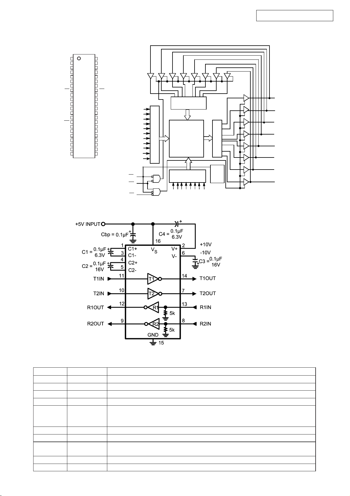
LMS202IMX (CV: IC705)
LMS202IMX Terminal Function
Pin Number Pin Name Pin Function
1, 3 C1+, C1− External capacitor connection pins. Recommended external capacitor C1 = 0.1µF (6.3V)
2 V+ Positive supply for TIA/EIA-232E drivers. Recommended external capacitor C4 = 0.1µF (6.3V)
4, 5 C2+, C2− External capacitor connection pins. Recommended external capacitor C2 = 0.1µF (16V)
6 V− Negative supply for TIA/EIA-232E drivers. Recommended external capacitor C3 = 0.1µF (16V)
7, 14 T1out, T2out Transmitter output pins conform to TIA/EIA-232E levels. The typical transmitter output swing is
±
8V when loaded 3kΩ load to ground. The open-circuit output voltage swings from (V+ − 0.6V)
to V−
8,13 R1in, R2in Receiver inputs accept TIA/EIA-232
9, 12 R1out and R2out Receiver output pins are TTL/CMOS compatible
10, 11 Tin1, Tin2 Transmitter input pins are TTL/CMOS compatible. Inputs of transmitter do not have pull-up
resistors. Connect all unused transmitter inputs to ground
15 GND Ground pin
16 V
S
Power supply pin for the device, +5V (±10%)
28
AVR-2805/985/AVC-2890
TC90A69F (VI: IC109)
COUT
VSS1
YOUT
VB2
PD
FIL
27
26
25
24
23
PLL DET 1/2VCO
Ped.
LPF
CLIP
22
1/8
28
DAC
INTERPOLATION
(8fsc)
DAC
CORING
PEAKING
ADC
1
2
3
4
5
6
7
BIAS VB1
VRT
VDD1
TESTI1
VSS2
VRB
YCIN
LC75721E (VI: IC701, 702)
G7 G8G9
G10
G11
AA8/G12
AA7/G13
AA6/G14
AA5/G15
AA4/G16
AA3
AA2
AA1
AM35
AM34
AM33
48 33
49
DI
CL
CE
RES
DD
V
OSCI
OSCO
Vss
TEST
FL
V
G1
G2
G3
G4
G5
G6
64
161
AM 1
AM 2
AM 3
AM 4
AM 5
AM 6
AM 7
AM 8
AM 9
AM 10
AM 11
AM 12
AM 13
AM 14
AM 15
AM 16
VSS4
21
8fsc 4fsc
KILLER
Sync. Clamp
8
TEST
32
17
VDD4
FSC
TESTOUT
MODE1
SDA
SCL
20
19
18
17
16
15
IIC BUS
CORING V-ENHANCER
DELAY
CNR
C-N.C
9
10
KILLER
MEMORY
TESTI2
LINE
LINE
MEMORY
DYNAMIC COMB FILTER
11
12
VSS3
VDD3
13
14
VDD2
TESTI3
LC75721E Terminal Function
Symbol
V
DD
Vss
AM 17
V
FL
AM 18
AM 19
AM 20
DI
AM 21
CL
AM 22
AM 23
CE
AM 24
AM 25
AM 26
OSCI
AM 27
OSCO
AM 28
AM 29
RES
AM 30
AM 31
AM1~AM35
AM 32
AA1~AA3
AA4/G16
AA5/G15
AA6/G14
AA7/G13
AA8/G12
G1~G11 Grid output terminal
TEST LSI test terminal
Function
Power terminal +5V
Power terminal GND
Power terminal FL drive
Serial data transfer terminal
DI: Data
CL: Clock
CE: Chip enable
External CR connecting terminal
System reset terminal
Anode output terminal
Anode/Grid output terminal
NJM2274R (VI: IC110)
1
2
TOP
3
VIEW
4
Power Save CTL
7
1Yin
Cin
8 Bias
Disc.
Clamp
7
C Mute CTL
Vref
8
7
6
5
Vcc
2
+
GND
+
2
750
ohm
3 Vout
Vsag4
TA1270BF (VI: IC111) TA8772AN (VI: IC501)
Except U.S.A., Canada & Japan model
INPUT30B-Y1
PEDESTAL
CLAMP
9
SYNC.
OUTPUT
INPUT29Y1
NOSE
DET
INPUT28I
YUV RGB
MATRIX
10
AFC
FILTER
2
11
SYNC.
GND
GND
R-Y2
27
SW
32fH
VCO
12
32fh VCO
INPUT26B-Y2
PEDESTAL
CLAMP
13
VD
INPUT25Y2
HI: 20h/LOW: 24h
SW
CP / HP
V C / D
14
HD
OUTPUT
OUTPUT
INPUT
IN
SCP
24
23
22
21
20
19
18
17
16
15
SW GND
ADRS SW
R-Y/R
OUTPUT
B-Y/B
OUTPUT
Y/G
OUTPUT
SW
Vcc (9V)
SYNC
Vcc (9V)
CP/HP
INPUT
Dig GND
SCP
OUTPUT
30 29 28 27 26 25 24 23 22 21 20 19 18 17 16
Clamp Clamp
1
1
××
××
1 or
1 or
2
Pulse
Elimination
2
Elimination
Pulse
Pulse
Insertion
Pulse
Insertion
+
+
1 2 3 4 5 6 7 8 9 10 11 12 13 14 15
DAC1
Y INPUT
DAC Vcc (5V)
C Vcc (5V)
UV/CbCr SW
fsc OUTPUT
1HDL CONT
SECAM CONT
B-Y/Cb OUTPUT
R-Y/Cr OUTPUT
DAC2
39
40
41
42
43
44
45
46
47
48
DAC237Y OUTPUT36GND35DAC
38
Y OFFSETSWDAC
DAC1
PEDESTAL
CLAMP
Y DL
fsc
1H DL
CONTROL
SECAM
CONTROL
CbCr / UV
SW
VCXO
1
X’tal
4.43MHz
TEST34SDA33SCL32Ys
TEST
SUB-
Y DL
CONTRAST
SW
fsc
TRAP
SYSTEM
LPF / fsc
TRAP
BPF H. AFC H C / D
APC
SUB-COLOR
2
3
4
X’tal
APC
M-X’tal
3.58MHz
I2C BUS
CONTROL
5
C GND
CW
MATRIX
P / N ID
SW
TOF
ACC
6
CHROMA
Ys
7
OUTPUT
(TH=0.7V
HI; 1IN/LOW; 2IN)31R-Y1
TINT
DEMO
CHROMA
BLK
V SEP
SYNC
SEP
V-SEP
OFFSET
SW
8
INPUT
SYNC.
C
29
AGC
Detector
AGC
Detector
Pulse
HG. GP
LPF LPF
AGC AGC
Clamp Clamp
Detector
1/225
225f
VCO
Bipolar Circuit
H
CCD Circuit
CCD 1H
Clock
REF REF
S / H S / H
Average
Bias
CCD 1H
Loading...