


ATF22V10BQL-20PC
ATMEL ATF22V10BQL-20PC, ATF22V10BQL-20NM-883, ATF22V10BQL-20JI, ATF22V10BQL-20JC, ATF22V10BQL-20GM-883 Datasheet
...
1
Features
•
Industry Standard Architecture
– Low Cost Easy-to-Use Software Tools
•
High-Speed, Electrically-Erasable Programmable Logic Devices
– 7.5 ns Maximum Pin-to-Pin Delay
•
Several Power Saving Options
•
CMOS and TTL Compatible Inputs and Outputs
– Input and I/O Pull-Up Resistors
•
Advanced Flash Technology
– Reprogrammable
– 100% Tested
•
High Reliability CMOS Process
– 20 Year Data Retention
– 100 Erase/Write Cycles
– 2,000V ESD Protection
– 200 mA Latchup Immunity
•
Full Military, Commercial, and Industrial Temperature Ranges
•
Dual-in-Line and Surface Mount Packages in Standard Pinouts
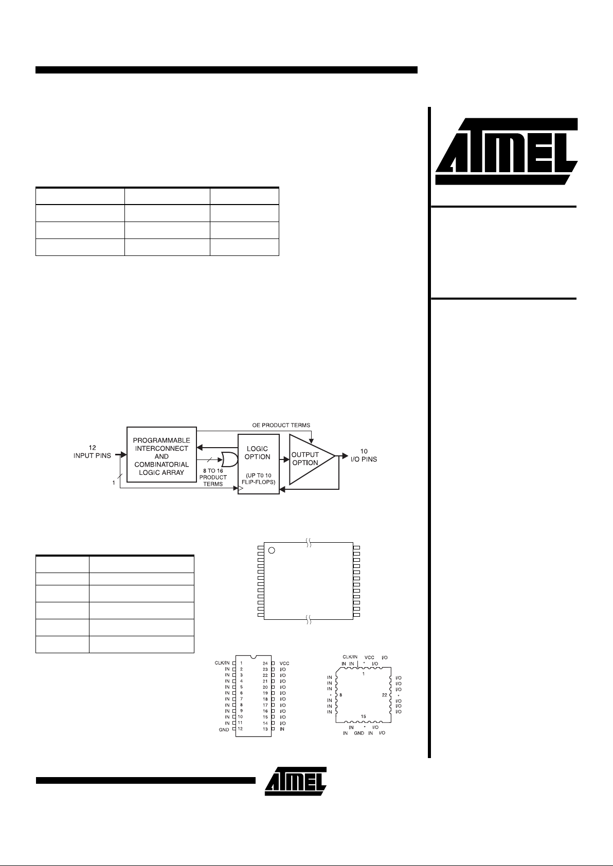
Logic Diagram
Device I
CC
, Stand-By I
CC
, Active
ATF22V10B 85 mA 90 mA
ATF22V10BQ 35 mA 40 mA
ATF22V10BQL 5 mA 20 mA
Rev. 0250F–05/98
High-
Performance
EE PLD
ATF22V10B
Pin Configurations
Pin Name Function
CLK Clock
IN Logic Inputs
I/O Bidirectional Buffers
* No Internal Connec tion
V
CC
+5V Supply
DIP/SOIC
TSSOP Top View
1
2
3
4
5
6
7
8
9
10
11
12
24
23
22
21
20
19
18
17
16
15
14
13
CLK/IN
IN
IN
IN
IN
IN
IN
IN
IN
IN
IN
GND
VCC
I/O
I/O
I/O
I/O
I/O
I/O
I/O
I/O
I/O
I/O
IN
LCC/PLCC
Top View
ATF22V10B
2
Description
The ATF22V10B is a hi gh pe rf ormance CMOS (Electrical ly
Erasable) Programmable Logic Device (PLD) which utilizes
Atmel’s proven electrically erasable Flash memory technol-
ogy. Speeds down to 7.5 ns and power dissipation as low
as 10 mA are offered. All speed ranges are specified over
the full 5V ± 10% range for mil itary and in dustrial tempera-
ture ranges, and 5V ± 5% for commercial temperature
ranges.
Several low power options allow selection of the best solu-
tion for various types of power-limited applications. Each of
these options significantly reduces total system power and
enhances system reliability.
Absolute Maximum Ratings*
Temperature Under Bias................................ -55°C to +125°C
*NOTICE: Stresses beyond those listed under “Absolute
Maximum Ratings” may cause permanent dam-
age to the dev ice. Th is is a s tress rating only an d
functional oper ati on of the device at these or an y
other conditions beyond those indicated in the
operational sections of this specification is not
implied. Exposure to absolute maximum rating
conditions f or e xtended periods ma y af fect dev ice
reliability .
Note: 1. Minimum voltage is -0.6V DC, which may under-
shoot to -2.0V for pulses of less than 20 ns. Max-
imum output pin voltage is V
CC
+ 0.75V DC,
which may overshoot to 7.0V for pulses of less
than 20 ns.
Storage Temperature.....................................-65°C to +150°C
Voltage on Any Pin with
Respect to Ground .........................................-2.0V to +7.0V
(1)
Voltage on Input Pins
with Respect to Ground
During Programming.....................................-2.0V to +14.0V
(1)
Programming Voltage with
Respect to Ground .......................................-2.0V to +14.0V
(1)
DC and AC Operating Conditions
Commercial Industrial Military
Operating Temperature (Case) 0°C - 70°C -40°C - 85°C -55°C - 125°C
V
CC
Power Supply 5V
±
5% 5V
±
10% 5V
±
10%
ATF22V10B
3
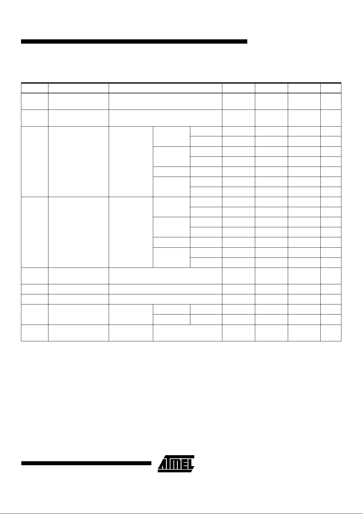
Notes: 1. Not more than one output at a time should be shorted. Duration of short circuit test should not exceed 30 sec.
DC Characteristics
Symbol Parameter Condition Min Typ Max Units
I
IL
Input or I/O
Low Leakage Current
0 ≤ V
IN
≤
V
IL
(MAX)
-35 -100 µA
I
IH
Input or I/O
High Leakage Current
3.5 ≤ V
IN
≤ V
CC
10 µA
I
CC
Power Supply Current,
Standby
V
CC
= MAX,
V
IN
= MAX,
Outputs Open
B-7, -10
Com. 85 120 mA
Ind., Mil. 85 140 mA
B-15, -25
Com. 65 90 mA
Ind., Mil. 65 115 mA
BQ-15 Com. 35 55 mA
BQL-20, -25
Com. 5 10 mA
Ind., Mil. 5 15 mA
I
CC2
Clocked Power
Supply Current
V
CC
= MAX,
Outputs Open,
f = 15 MHz
B-7, -10
Com. 90 120 mA
Ind., Mil. 90 145 mA
B-15, -25
Com. 65 90 mA
Ind., Mil. 65 120 mA
BQ-15 Com. 40 60 mA
BQL-20, -25
Com. 20 50 mA
Ind., Mil. 20 70 mA
I
OS
(1)
Output Short
Circuit Current
V
OUT
= 0.5V -130 mA
V
IL
Input Low Voltage -0.5 0.8 V
V
IH
Input High Voltage 2.0 V
CC
+ 0.75 V
V
OL
Output Low Voltage
V
IN
= V
IH
or V
IL
,
V
CC
= MIN
I
OL
= 16 mA Com., Ind. 0.5 V
I
OL
= 12 mA Mil. 0.5 V
V
OH
Output High Voltage
V
IN
= V
IH
or V
IL
,
V
CC
= MIN
I
OH
= -4.0 mA 2.4 V
ATF22V10B
4
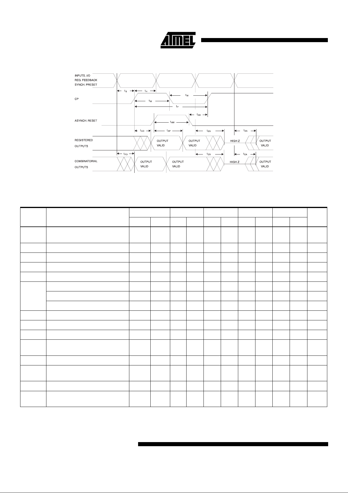
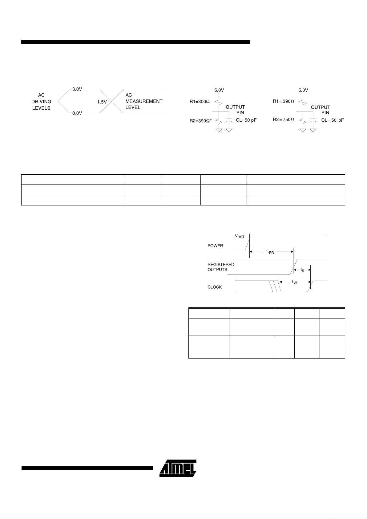
AC Waveforms
(1)
Note: 1. Timing measurement reference is 1.5V. Input AC driving levels are 0.0V and 3.0V, unless otherwise specified.
Notes: 1. See ordering informat ion for valid part numbers.
2. 5.5 ns for DIP package devices.
3. 111 MHz for DIP package devices.
AC Characteristics
(1)
Symbol Parameter
-7 -10 -15 -20 -25
UnitsMin Max Min Max Min Max Min Max Min Max
t
PD
Input or Feedback to
Combinatorial Output
3 7.5310315320325 ns
t
CO
Clock to Output 2 4.5
(2)
26.528212215ns
t
CF
Clock to Feedback 2.5 2.5 2.5 8 13 ns
t
S
Input or Feedback Setup Time 3.5 4.5 10 14 15 ns
t
H
Hold Time 0 0 0 0 0 ns
F
MAX
External Feedback 1/(t
S
+ t
CO
) 125
(3)
90 55.5 38.5 33.3 MHz
Internal Feedback 1/(t
S
+ t
CF
) 166 142 69 45.5 40 M Hz
No Feedback 1/(t
WH
+ t
WL
) 166 142 83.3 38.5 MHz
t
W
Clock Width (t
WL
and t
WH
) 3 3.5 6 10 13 ns
t
EA
Input or I/O to Output Enable 3 7.5 3 10 3 15 3 20 3 25 ns
t
ER
Input or I/O to Output Disable 3 7.5 3 9 3 15 3 20 3 25 ns
t
AP
Input or I/O to Asynchronous
Reset of Register
3 10312320322325ns
t
AW
Asynchronous Reset Width 7 8 15 20 25 ns
t
AR
Asynchronous Reset
Recovery Time
5 6 10 20 25 ns
t
SP
Setup Time, Synchronous Preset 4.5 6 10 14 15 ns
t
SPR
Synchronous Preset to
Clock Recovery Time
5 8 10 14 15 ns
ATF22V10B
5
Input Test Waveforms and
Measurement Levels
t
R
, t
F
< 3 ns
Outout Test Loads
* All except -7 which is R2 = 300
Ω
Note: 1. Typical values for nominal supply voltage. This parameter is only sampled and is not 100% tested.
Power Up Reset
The register s in the ATF 22V10Bs are design ed to reset
during power up. At a point delayed slightly from V
CC
crossing V
RST
, all registers will be reset to the low state.
The output state will depend on the polarity of the output
buffer.
This feature is critical for state machine initialization. How-
ever, due to the asynchronous nature of reset and the
uncertainty of h ow V
CC
actually rises in the sys tem, the fo l-
lowing conditions are required:
1. The V
CC
rise must be monotonic,
2. After reset occurs, all input and feedback setup times
must be met before driving the clock pin high, and
3. The clock must remain stable during t
PR
.
Preload of Registered Outputs
The ATF22V10B’s registers are provided with circuitry to
allow loading of each register with either a high or a low.
This feature will simplify testing since an y state can be
forced into the registers to control test seq uencing. A
JEDEC file with preload is generated whe n a source fil e
with vectors is compiled. Once downloaded, the JEDEC file
preload sequence will be done automatically by most of the
approved programmers after the programming.
Security Fuse Usage
A single fuse is provided to prevent unauthoriz ed copying
of the ATF22V10B fuse patterns. Once programmed, fuse
verify and preload are inhibited. However, the 64-bit User
Signature remains accessible.
The security fuse should be programmed last, as its effect
is immediate.
Commercial
Military
Pin Capacitance
f = 1 MHz, T = 25°C
(1)
T yp Max Units Conditions
C
IN
58 pFV
IN
= 0V
C
OUT
68 pFV
OUT
= 0V
Parameter Description Typ Max Units
t
PR
Powe r-Up
Reset Time
600 1,000 ns
V
RST
Power-Up
Reset
Voltage
3.8 4.5 V
 Loading...