


 Loading...
BDTIC www.bdtic.com/ATMEL
|
|
|
|
|
|
|
|
Features |
|
|
|
|
|
|
|
• |
Incorporates the ARM920T™ ARM® Thumb® Processor |
|
|
|
|
|
|
|
– 200 MIPS at 180 MHz, Memory Management Unit |
|
|
|
|
|
|
|
– 16-KByte Data Cache, 16-KByte Instruction Cache, Write Buffer |
|
|
|
|
|
|
|
– In-circuit Emulator including Debug Communication Channel |
|
|
|
|
|
|
|
– Mid-level Implementation Embedded Trace Macrocell™ (256-ball BGA Package |
|
|
|
|
|
|
|
only) |
|
|
|
|
|
|
• |
Low Power: On VDDCORE 24.4 mA in Normal Mode, 520 µA in Standby Mode |
|
|
|
|
|
|
|
|
|
|
|
|
||
• |
Additional Embedded Memories |
|
ARM920T-based |
||||
|
– 16K Bytes of SRAM and 128K Bytes of ROM |
|
|||||
• |
External Bus Interface (EBI) |
|
Microcontroller |
||||
|
– Supports SDRAM, Static Memory, Burst Flash, Glueless Connection to |
|
|||||
• |
CompactFlash® and NAND Flash/SmartMedia® |
|
|
|
|
|
|
System Peripherals for Enhanced Performance: |
|
AT91RM9200 |
|||||
|
– Enhanced Clock Generator and Power Management Controller |
|
|||||
–Two On-chip Oscillators with Two PLLs
–Very Slow Clock Operating Mode and Software Power Optimization Capabilities
–Four Programmable External Clock Signals
–System Timer Including Periodic Interrupt, Watchdog and Second Counter
–Real-time Clock with Alarm Interrupt
–Debug Unit, Two-wire UART and Support for Debug Communication Channel
–Advanced Interrupt Controller with 8-level Priority, Individually Maskable Vectored Interrupt Sources, Spurious Interrupt Protected
–Seven External Interrupt Sources andMacshbM·One Fast Interrupt Sour e
–Four 32-bit PIO Controllers with Up to 122 Programm ble I/O Lines, Input Change Interrupt and Open-drain Capability on Each Line
–20-channel Peripheral DMA Controller (PDC)
•Ethernet MAC 10/100 Base-T
–Media Independent Interface (MII) or Reduced Media Independent Interface (RMII)
–Integrated 28-byte FIFOs and Dedicated DMA Channels for Receive and Transmit
•USB 2.0 Full Speed (12 Mbits per second) Host Double Port
–Dual On-chip Transceivers (Single Port Only on 208-lead PQFP Package)
–Integrated FIFOs and Dedicated DMA Channels
•USB 2.0 Full Speed (12 Mbits per second) Device Port
–On-chip Transceiver, 2-Kbyte Configurable Integrated FIFOs
•Multimedia Card Interface (MCI)
–Automatic Protocol Control and Fast Automatic Data Transfers
–MMC and SD Memory Card-compliant, Supports Up to Two SD Memory Cards
•Three Synchronous Serial Controllers (SSC)
–Independent Clock and Frame Sync Signals for Each Receiver and Transmitter
–I2S Analog Interface Support, Time Division Multiplex Support
–High-speed Continuous Data Stream Capabilities with 32-bit Data Transfer
•Four Universal Synchronous/Asynchronous Receiver/Transmitters (USART)
– Support for ISO7816 T0/T1 Smart Card |
NOTE: This is a summary document. |
|||||
The complete document is available on |
||||||
– Hardware Handshaking |
||||||
the Atmel website at www.atmel.com. |
||||||
– RS485 Support, IrDA® Up To 115 Kbps |
|
|||||
– Full Modem Control Lines on USART1 |
|
|||||
• Master/Slave Serial Peripheral Interface (SPI) |
|
|||||
– 8- to 16-bit Programmable Data Length, 4 External Peripheral Chip Selects |
1768LS–ATARM–16-Jun-09 |
|||||
|
|
|
|
|
||
|
|
|
|
|
|
|
|
|
|
|
|
|
|
|
|
|
|
|
|
|

•Two 3-channel, 16-bit Timer/Counters (TC)
–Three External Clock Inputs, Two Multi-purpose I/O Pins per Channel
–Double PWM Generation, Capture/Waveform Mode, Up/Down Capability
•Two-wire Interface (TWI)
–Master Mode Support, All 2-wire Atmel EEPROMs Supported
•IEEE® 1149.1 JTAG Boundary Scan on All Digital Pins Power Supplies
–1.65V to 1.95V for VDDCORE, VDDOSC and VDDPLL
–3.0V to 3.6V for VDDIOP (Peripheral I/Os) and for VDDIOM (Memory I/Os) Available in a 208-pin Green PQFP or 256-ball RoHS-compliant BGA Package
1. Description
The AT91RM9200 is a complete system-on-chip built around the ARM920T ARM Thumb processor. It incorporates a rich set of system and application peripherals and standard interfaces in order to provide a single-chip solution for a wide range of compute-intensive applications that require maximum functionality at minimum power consumption at lowest cost.
The AT91RM9200 incorporates a high-speed on-chip SRAM workspace, and a low-latency External Bus Interface (EBI) for seamless connection to whatever configuration of off-chip memories and memory-mapped peripherals is required by the application. The EBI incorporates controllers for synchronous DRAM (SDRAM), Burst Flash and Static memories and features specific circuitry facilitating the interface for NAND Flash/SmartMedia and Compact Flash.
The Advanced Interrupt Controller (AIC) enhances the interrupt handling performance of the
ARM920T processorMacshbM·by providing multiple ve tored, prioritized interrupt sources and reducing the time taken to transfer to n interrupt handler.
The Peripheral DMA Controller (PDC) provides DMA channels for all the serial peripherals, enabling them to transfer data to or from onand off-chip memories without processor intervention. This reduces the processor overhead when dealing with transfers of continuous data streams.The AT91RM9200 benefits from a new generation of PDC which includes dual pointers that simplify significantly buffer chaining.
The set of Parallel I/O (PIO) controllers multiplex the peripheral input/output lines with generalpurpose data I/Os for maximum flexibility in device configuration. An input change interrupt, open drain capability and programmable pull-up resistor is included on each line.
The Power Management Controller (PMC) keeps system power consumption to a minimum by selectively enabling/disabling the processor and various peripherals under software control. It uses an enhanced clock generator to provide a selection of clock signals including a slow clock (32 kHz) to optimize power consumption and performance at all times.
The AT91RM9200 integrates a wide range of standard interfaces including USB 2.0 Full Speed Host and Device and Ethernet 10/100 Base-T Media Access Controller (MAC), which provides connection to a extensive range of external peripheral devices and a widely used networking layer. In addition, it provides an extensive set of peripherals that operate in accordance with several industry standards, such as those used in audio, telecom, Flash Card, infrared and Smart Card applications.
To complete the offer, the AT91RM9200 benefits from the integration of a wide range of debug features including JTAG-ICE, a dedicated UART debug channel (DBGU) and an embedded real time trace. This enables the development and debug of all applications, especially those with real-time constraints.
2 AT91RM9200 
1768LS–ATARM–16-Jun-09

AT91RM9200
2. Block Diagram
Bold arrows (  ) indicate master-to-slave dependency.
Figure 2-1. AT91RM9200 Block Diagram
TST0-TST1 |
|
|
Reset |
|
|
|
|
|
|
|
|
|
|
|
|||||
|
|
|
|
|
|
|
|
|
|
|
|
|
|
|
|
||||
NRST |
|
|
|
and |
|
|
|
|
|
|
|
|
|
|
|
||||
|
|
Test |
|
|
|
ARM920T Core |
|
|
|
|
|
TSYNC |
|||||||
|
|
|
|
|
|
|
|
|
|
|
|
|
|
|
|||||
JTAGSEL |
|
|
|
|
|
|
|
|
|
ICE |
|
|
|
|
ETM |
|
PIO |
|
TCLK |
|
|
|
|
|
|
|
|
|
|
|
|
|
|
|
|||||
|
|
|
|
|
|
|
|
|
|
|
|
|
|
|
TPS0 - TPS2 |
||||
|
|
|
|
|
|
|
|
|
|
|
|
|
|
|
|
||||
TDI |
|
|
|
JTAG |
|
|
|
|
|
|
|
|
|
|
|||||
|
|
|
|
|
|
|
|
|
|
|
|
|
|
|
|||||
TDO |
|
|
|
|
|
|
|
|
|
Instruction Cache |
|
|
Data Cache |
|
|
|
|
TPK0 - TPK15 |
|
|
|
|
|
|
|
|
|
|
|
|
|
|
|
|
|
|
|||
TMS |
|
|
|
Scan |
|
MMU |
|
|
|||||||||||
TCK |
|
|
|
|
|
|
|
|
|
|
16K bytes |
|
|
16K bytes |
|
|
|
|
|
|
|
|
|
|
|
|
|
|
|
|
|
|
|
|
|||||
|
|
|
|
|
|
|
|
|
|
|
|
|
|
|
|
|
|
||
NTRST |
|
|
|
|
|
|
|
|
|
|
|
|
|
|
|
|
|
|
|
|
|
|
|
|
|
|
BMS |
|
|
|
|
|
|
|
D0-D15 |
FIQ |
PIO |
|
|
Address |
|
|
A0/NBS0 |
|
AIC |
Fast SRAM |
|
|
A1/NBS2/NWR2 |
||
IRQ0-IRQ6 |
|
16K bytes |
Decoder |
EBI |
|
A2-A15/A18-A22 |
|
|
|
|
|||||
|
|
|
|
|
A16/BA0 |
||
PCK0-PCK3 |
|
|
|
|
|
|
|
|
|
|
Abort |
CompactFlash |
|
A17/BA1 |
|
PLLRCB |
PLLB |
|
|
NAND Flash |
|
NCS0/BFCS |
|
|
|
Status |
SmartMedia |
|
NCS1/SDCS |
||
PLLRCA |
PLLA |
|
Fast ROM |
|
|
|
NCS2 |
|
|
|
|
NCS3/SMCS |
|||
|
128K bytes |
|
|
|
|||
|
|
|
Misalignment |
|
|
NRD/NOE/CFOE |
|
XIN |
|
PMC |
|
|
|
||
OSC |
|
Detector |
|
|
NWR0/NWE/CFWE |
||
|
|
|
|
|
NWR1/NBS1/CFIOR |
||
XOUT |
|
|
|
|
|
||
|
|
|
|
|
|
NWR3/NBS3/CFIOW |
|
|
|
|
Peripheral |
Bus |
|
|
SDCK |
|
|
|
Bridge |
Arbiter |
|
|
SDCKE |
|
|
|
SDRAM |
|
RAS-CAS |
||
|
|
|
|
|
|
||
|
|
System |
|
|
Controller |
|
SDWE |
|
|
Timer |
Peripheral |
|
|
|
SDA10 |
|
|
|
|
|
BFRDY/SMOE |
||
|
|
|
DMA |
|
|
|
|
|
|
|
|
|
|
BFCK |
|
|
|
|
Controller |
Memory |
Burst |
|
BFAVD |
|
|
|
|
Controller |
|
BFBAA/SMWE |
|
XIN32 |
|
|
|
Flash |
|
||
|
|
|
|
BFOE |
|||
XOUT32 |
OSC |
RTC |
|
|
Controller |
PIO |
BFWE |
|
|
|
|
|
A23-A24 |
||
|
|
|
|
|
|
|
A25/CFRNW |
DRXD |
|
|
|
|
Static |
|
NWAIT |
|
DBGU |
|
|
|
NCS4/CFCS |
||
|
|
|
Memory |
|
|||
|
|
|
|
|
|
NCS5/CFCE1 |
|
DTXD |
|
PDC |
|
|
Controller |
|
|
PIO |
|
|
|
NCS6/CFCE2 |
|||
|
|
|
|
|
|
NCS7 |
|
|
|
PIOA/PIOB/PIOC/PIOD |
|
|
|
D16-D31 |
|
|
|
|
|
|
|
||
|
|
Controller |
|
|
|
|
HDMA |
|
|
|
|
DMA |
FIFO |
|
|
|
|
|
|
|
HDPA |
||
|
|
|
|
|
|
|
|
|
|
FIFO |
|
USB Ho t |
|
HDMB |
|
DDM |
|
|
|
|
|||
MacshbM·Transceiver HDPB |
|||||||
DDP |
Transceiver |
USB Device |
|
|
|
|
|
|
|
|
DMA |
FIFO |
|
|
|
|
|
|
|
|
|
|
ETXCK-ERXCK-EREFCK |
MCCK |
|
|
|
|
|
|
ETXEN-ETXER |
|
|
|
|
|
|
ECRS-ECOL |
|
MCCDA |
|
|
|
|
|
|
|
|
|
|
|
|
|
ERXER-ERXDV |
|
MCDA0-MCDA3 |
|
MCI |
|
|
|
|
|
|
|
Ethernet MAC 10/100 |
|
ERX0-ERX3 |
|||
MCCDB |
|
|
|
|
|||
|
|
|
|
|
|
ETX0-ETX3 |
|
MCDB0-MCDB3 |
|
|
PDC |
|
|
|
|
|
|
|
|
|
EMDC |
||
|
|
|
|
|
|
||
|
|
|
|
|
|
|
EMDIO |
RXD0 |
|
|
|
|
|
|
EF100 |
TXD0 |
|
|
|
APB |
|
|
TF0 |
SCK0 |
|
USART0 |
|
|
|
|
|
|
|
|
|
|
TK0 |
||
RTS0 |
|
|
|
|
|
|
TD0 |
CTS0 |
|
|
PDC |
|
SSC0 |
|
|
|
|
|
|
RD0 |
|||
|
|
|
|
|
|||
RXD1 |
|
|
|
|
|
|
RK0 |
|
|
|
PDC |
|
|
RF0 |
|
TXD1 |
|
|
|
|
|
||
|
|
|
|
|
|
||
SCK1 |
|
|
|
|
|
|
TF1 |
RTS1 |
|
|
|
|
|
|
|
|
|
|
|
|
|
TK1 |
|
CTS1 |
|
USART1 |
|
|
|
|
|
|
|
|
|
|
TD1 |
||
DSR1 |
PIO |
|
|
|
SSC1 |
PIO |
RD1 |
DTR1 |
|
|
|
||||
|
|
|
|
RK1 |
|||
DCD1 |
|
|
|
PDC |
|
|
RF1 |
RI1 |
|
|
PDC |
|
|
||
|
|
|
|
|
|||
RXD2 |
|
|
|
|
|
|
TF2 |
|
|
|
|
|
|
TK2 |
|
TXD2 |
|
|
|
|
|
|
|
|
|
|
|
|
|
TD2 |
|
SCK2 |
|
USART2 |
|
|
SSC2 |
|
|
|
|
|
|
RD2 |
|||
RTS2 |
|
|
|
|
|
|
RK2 |
CTS2 |
|
|
PDC |
|
|
|
|
|
|
PDC |
|
|
RF2 |
||
|
|
|
|
|
|||
RXD3 |
|
|
|
|
|
|
TCLK0 |
TXD3 |
|
|
|
Timer Counter |
|
||
SCK3 |
|
USART3 |
|
|
TCLK1 |
||
|
|
|
|
|
|||
RTS3 |
|
|
|
|
|
|
TCLK2 |
CTS3 |
|
|
PDC |
|
TC0 |
|
TIOA0 |
|
|
|
|
|
TIOB0 |
||
NPCS0 |
|
|
|
|
TC1 |
|
TIOA1 |
|
|
|
|
|
TIOB1 |
||
NPCS1 |
|
|
|
|
TC2 |
|
TIOA2 |
NPCS2 |
|
|
|
|
|
TIOB2 |
|
NPCS3 |
|
SPI |
|
|
|
|
|
MISO |
|
|
|
|
|
|
TCLK3 |
MOSI |
|
|
|
Timer Counter |
|
TCLK4 |
|
SPCK |
|
|
PDC |
|
|
|
TCLK5 |
|
|
|
|
|
TC3 |
|
TIOA3 |
TWD |
|
|
|
|
|
TIOB3 |
|
|
TWI |
|
|
TC4 |
|
TIOA4 |
|
TWCK |
|
|
|
|
TIOB4 |
||
|
|
|
|
TC5 |
|
TIOA5 |
|
|
|
|
|
|
|
TIOB5 |
|
|
|
|
|
|
|
|
|
|
|
|
|
|
|
|
3 |
1768LS–ATARM–16-Jun-09 |
|
|
|
|
|
|
|
3. Signal Description
Table 3-1. |
Signal Description by Peripheral |
|
|
|
|
|
||
|
|
|
|
|
|
Active |
|
|
Pin Name |
|
Function |
|
Type |
Level |
Comments |
|
|
|
|
|
|
|
|
|
|
|
|
|
|
|
Power |
|
|
|
|
|
|
|
|
|
|
|
|
|
VDDIOM |
|
|
Memory I/O Lines Power Supply |
|
Power |
|
3.0V to 3.6V |
|
|
|
|
|
|
|
|
|
|
VDDIOP |
|
|
Peripheral I/O Lines Power Supply |
|
Power |
|
3.0V to 3.6V |
|
|
|
|
|
|
|
|
|
|
VDDPLL |
|
|
Oscillator and PLL Power Supply |
|
Power |
|
1.65V to 1.95V |
|
|
|
|
|
|
|
|
|
|
VDDCORE |
|
Core Chip Power Supply |
|
Power |
|
1.65V to 1.95V |
|
|
|
|
|
|
|
|
|
|
|
VDDOSC |
|
Oscillator Power Supply |
|
Power |
|
1.65V to 1.95V |
|
|
|
|
|
|
|
|
|
|
|
GND |
|
|
Ground |
|
Ground |
|
|
|
|
|
|
|
|
|
|
|
|
GNDPLL |
|
|
PLL Ground |
|
Ground |
|
|
|
|
|
|
|
|
|
|
|
|
GNDOSC |
|
Oscillator Ground |
|
Ground |
|
|
|
|
|
|
|
|
|
|
|
|
|
|
|
|
Clocks, Oscillators and PLLs |
|
|
|
||
|
|
|
|
|
|
|
|
|
XIN |
|
|
Main Crystal Input |
|
Input |
|
|
|
|
|
|
|
|
|
|
|
|
XOUT |
|
|
Main Crystal Output |
|
Output |
|
|
|
|
|
|
|
|
|
|
|
|
XIN32 |
|
|
32KHz Crystal Input |
|
Input |
|
|
|
|
|
|
|
|
|
|
|
|
XOUT32 |
|
|
32KHz Crystal Output |
|
Output |
|
|
|
|
|
|
|
|
|
|
|
|
PLLRCA |
|
|
PLL A Filter |
|
Input |
|
|
|
|
|
|
|
|
|
|
||
PLLRCB |
MacshbM· |
|
||||||
|
|
PLL B Filter |
|
Input |
|
|
|
|
PCK0 - PCK3 |
|
Programmable Clock Output |
|
Output |
|
|
|
|
|
|
|
|
ICE and JTAG |
|
|
|
|
|
|
|
|
|
|
|
|
|
TCK |
|
|
Test Clock |
|
Input |
|
Schmitt trigger |
|
|
|
|
|
|
|
|
|
|
TDI |
|
|
Test Data In |
|
Input |
|
Internal Pull-up, Schmitt trigger |
|
|
|
|
|
|
|
|
|
|
TDO |
|
|
Test Data Out |
|
Output |
|
Tri-state |
|
|
|
|
|
|
|
|
|
|
TMS |
|
|
Test Mode Select |
|
Input |
|
Internal Pull-up, Schmitt trigger |
|
|
|
|
|
|
|
|
|
|
NTRST |
|
|
Test Reset Signal |
|
Input |
Low |
Internal Pull-up, Schmitt trigger |
|
|
|
|
|
|
|
|
|
|
JTAGSEL |
|
JTAG Selection |
|
Input |
|
Schmitt trigger |
|
|
|
|
|
|
|
|
|
|
|
|
|
|
|
ETM™ |
|
|
|
|
TSYNC |
|
|
Trace Synchronization Signal |
|
Output |
|
|
|
|
|
|
|
|
|
|
|
|
TCLK |
|
|
Trace Clock |
|
Output |
|
|
|
|
|
|
|
|
|
|
|
|
TPS0 - TPS2 |
|
Trace ARM Pipeline Status |
|
Output |
|
|
|
|
|
|
|
|
|
|
|
|
|
TPK0 - TPK15 |
|
Trace Packet Port |
|
Output |
|
|
|
|
|
|
|
|
|
|
|
|
|
|
|
|
|
Reset/Test |
|
|
|
|
|
|
|
|
|
|
|
|
|
NRST |
|
|
Microcontroller Reset |
|
Input |
Low |
No on-chip pull-up, Schmitt trigger |
|
|
|
|
|
|
|
|
|
|
TST0 - TST1 |
|
Test Mode Select |
|
Input |
|
Must be tied low for normal |
|
|
|
|
|
operation, Schmitt trigger |
|
||||
|
|
|
|
|
|
|
|
|
|
|
|
|
|
|
|
|
|
4 AT91RM9200
1768LS–ATARM–16-Jun-09

|
|
|
|
|
|
|
|
AT91RM9200 |
|
|
|
|
|
|
|
|
|
||
|
Table 3-1. |
Signal Description by Peripheral |
|
|
|
|
|||
|
|
|
|
|
|
|
|||
|
|
|
|
|
|
|
|||
|
|
|
|
|
|
|
|
|
|
|
|
|
|
|
|
Active |
|
|
|
|
Pin Name |
|
Function |
|
Type |
Level |
Comments |
|
|
|
|
|
|
|
|
|
|
|
|
|
|
|
|
Memory Controller |
|
|
|
|
|
|
|
|
|
|
|
|
|
|
|
|
BMS |
|
Boot Mode Select |
|
Input |
|
|
|
|
|
|
|
|
|
|
|
|
|
|
|
|
|
|
Debug Unit |
|
|
|
|
|
|
|
|
|
|
|
|
|
|
|
|
DRXD |
|
Debug Receive Data |
|
Input |
|
Debug Receive Data |
|
|
|
|
|
|
|
|
|
|
|
|
|
DTXD |
|
Debug Transmit Data |
|
Output |
|
Debug Transmit Data |
|
|
|
|
|
|
|
|
|
|
|
|
|
|
|
|
AIC |
|
|
|
|
|
|
|
|
|
|
|
|
|
|
|
|
IRQ0 - IRQ6 |
|
External Interrupt Inputs |
|
Input |
|
|
|
|
|
|
|
|
|
|
|
|
|
|
|
FIQ |
|
Fast Interrupt Input |
|
Input |
|
|
|
|
|
|
|
|
|
|
|
|
|
|
|
|
|
|
PIO |
|
|
|
|
|
|
|
|
|
|
|
|
|
|
|
|
PA0 - PA31 |
|
Parallel IO Controller A |
|
I/O |
|
Pulled-up input at reset |
|
|
|
|
|
|
|
|
|
|
|
|
|
PB0 - PB29 |
|
Parallel IO Controller B |
|
I/O |
|
Pulled-up input at reset |
|
|
|
|
|
|
|
|
|
|
|
|
|
PC0 - PC31 |
|
Parallel IO Controller C |
|
I/O |
|
Pulled-up input at reset |
|
|
|
|
|
|
|
|
|
|
|
|
|
PD0 - PD27 |
|
Parallel IO Controller D |
|
I/O |
|
Pulled-up input at reset |
|
|
|
|
|
|
|
|
|
|
|
|
|
|
|
|
EBI |
|
|
|
|
|
|
|
|
|
|
|
|
|
|
|
|
D0 - D31 |
|
Data Bus |
|
I/O |
|
Pulled-up input at reset |
|
|
|
|
|
|
|
|
|
|
|
|
|
A0 - A25 |
|
Address Bus |
|
Output |
|
0 at reset |
|
|
|
|
|
|
|
|
|
|
|
|
|
|
|
|
SMC |
|
|
|
|
|
|
|
|
|
|
|
||||
|
MacshbM· |
|
|||||||
|
NCS0 - NCS7 |
|
Chip Select Lines |
|
Output |
Low |
1 at reset |
|
|
|
NWR0 - NWR3 |
Write Signal |
|
Output |
Low |
1 at reset |
|
||
|
|
|
|
|
|
|
|
|
|
|
NOE |
|
Output Enable |
|
Output |
Low |
1 at reset |
|
|
|
|
|
|
|
|
|
|
|
|
|
NRD |
|
Read Signal |
|
Output |
Low |
1 at reset |
|
|
|
|
|
|
|
|
|
|
|
|
|
NUB |
|
Upper Byte Select |
|
Output |
Low |
1 at reset |
|
|
|
|
|
|
|
|
|
|
|
|
|
NLB |
|
Lower Byte Select |
|
Output |
Low |
1 at reset |
|
|
|
|
|
|
|
|
|
|
|
|
|
NWE |
|
Write Enable |
|
Output |
Low |
1 at reset |
|
|
|
|
|
|
|
|
|
|
|
|
|
NWAIT |
|
Wait Signal |
|
Input |
Low |
|
|
|
|
|
|
|
|
|
|
|
|
|
|
NBS0 - NBS3 |
|
Byte Mask Signal |
|
Output |
Low |
1 at reset |
|
|
|
|
|
|
|
|
|
|
|
|
|
|
|
EBI for CompactFlash Support |
|
|
|
|
||
|
|
|
|
|
|
|
|
|
|
|
CFCE1 - CFCE2 |
CompactFlash Chip Enable |
|
Output |
Low |
|
|
|
|
|
|
|
|
|
|
|
|
|
|
|
CFOE |
|
CompactFlash Output Enable |
|
Output |
Low |
|
|
|
|
|
|
|
|
|
|
|
|
|
|
CFWE |
|
CompactFlash Write Enable |
|
Output |
Low |
|
|
|
|
|
|
|
|
|
|
|
|
|
|
CFIOR |
|
CompactFlash IO Read |
|
Output |
Low |
|
|
|
|
|
|
|
|
|
|
|
|
|
|
CFIOW |
|
CompactFlash IO Write |
|
Output |
Low |
|
|
|
|
|
|
|
|
|
|
|
|
|
|
CFRNW |
|
CompactFlash Read Not Write |
|
Output |
|
|
|
|
|
|
|
|
|
|
|
|
|
|
|
CFCS |
|
CompactFlash Chip Select |
|
Output |
Low |
|
|
|
|
|
|
|
|
|
|
|
|
|
5
1768LS–ATARM–16-Jun-09

Table 3-1. |
|
|
|
|
|
|
|
|
|
|
|
|
|
|
|
|
|
|
|
|
|
|
|
|
|
||
Signal Description by Peripheral |
|
|
|
|
|
|
|
||||||
|
|
|
|
|
|
|
|
|
|
|
|
|
|
|
|
|
|
|
|
|
|
|
|
Active |
|
|
|
Pin Name |
|
Function |
|
Type |
|
Level |
Comments |
|
|||||
|
|
|
|
|
|
|
|
|
|
|
|
||
|
|
|
EBI for NAND Flash/SmartMedia Support |
|
|
|
|
||||||
|
|
|
|
|
|
|
|
|
|
|
|
||
SMCS |
|
|
NAND Flash/SmartMedia Chip Select |
|
Output |
|
Low |
|
|
|
|||
|
|
|
|
|
|
|
|
|
|
|
|
||
SMOE |
|
|
NAND Flash/SmartMedia Output Enable |
|
Output |
|
Low |
|
|
|
|||
|
|
|
|
|
|
|
|
|
|
|
|
||
SMWE |
|
|
NAND Flash/SmartMedia Write Enable |
|
Output |
|
Low |
|
|
|
|||
|
|
|
|
|
|
|
|
|
|
|
|
|
|
|
|
|
SDRAM Controller |
|
|
|
|
|
|
|
|||
|
|
|
|
|
|
|
|
|
|
|
|
|
|
SDCK |
|
|
SDRAM Clock |
|
Output |
|
|
|
|
|
|||
|
|
|
|
|
|
|
|
|
|
|
|
||
SDCKE |
|
|
SDRAM Clock Enable |
|
Output |
|
High |
|
|
|
|||
|
|
|
|
|
|
|
|
|
|
|
|
||
SDCS |
|
|
SDRAM Controller Chip Select |
|
Output |
|
Low |
|
|
|
|||
|
|
|
|
|
|
|
|
|
|
|
|
||
BA0 - BA1 |
|
Bank Select |
|
Output |
|
|
|
|
|
||||
|
|
|
|
|
|
|
|
|
|
|
|
||
SDWE |
|
|
SDRAM Write Enable |
|
Output |
|
Low |
|
|
|
|||
|
|
|
|
|
|
|
|
|
|
|
|||
RAS - CAS |
|
Row and Column Signal |
|
Output |
|
Low |
|
|
|
||||
|
|
|
|
|
|
|
|
|
|
|
|
|
|
SDA10 |
|
|
SDRAM Address 10 Line |
|
Output |
|
|
|
|
|
|||
|
|
|
|
|
|
|
|
|
|
|
|
||
|
|
|
Burst Flash Controller |
|
|
|
|
||||||
|
|
|
|
|
|
|
|
|
|
|
|
|
|
BFCK |
|
|
Burst Flash Clock |
|
Output |
|
|
|
|
|
|||
|
|
|
|
|
|
|
|
|
|
|
|
||
BFCS |
|
|
Burst Flash Chip Select |
|
Output |
|
Low |
|
|
|
|||
|
|
|
|
|
|
|
|
|
|
|
|
||
BFAVD |
|
|
Burst Flash Address Valid |
|
Output |
|
Low |
|
|
|
|||
|
|
|
|
|
|
|
|
|
|
|
|
||
BFBAA |
|
|
Burst Flash Address Advance |
|
Output |
|
Low |
|
|
|
|||
|
|
|
|
|
|
|
|
|
|||||
BFOE |
MacshbM· |
|
|
||||||||||
|
|
Burst Flash Output Enable |
Output |
Low |
|
||||||||
BFRDY |
|
|
Burst Flash Ready |
Input |
High |
|
|
||||||
|
|
|
|
|
|
|
|
|
|
||||
BFWE |
|
|
Burst Flash Write Enable |
Output |
Low |
|
|
||||||
|
|
|
|
|
|
|
|
|
|
|
|
||
|
|
|
Multimedia Card Interface |
|
|
|
|
||||||
|
|
|
|
|
|
|
|
|
|
|
|
|
|
MCCK |
|
|
Multimedia Card Clock |
|
Output |
|
|
|
|
|
|||
|
|
|
|
|
|
|
|
|
|
|
|
|
|
MCCDA |
|
|
Multimedia Card A Command |
|
I/O |
|
|
|
|
|
|||
|
|
|
|
|
|
|
|
|
|
|
|||
MCDA0 - MCDA3 |
Multimedia Card A Data |
|
I/O |
|
|
|
|
|
|||||
|
|
|
|
|
|
|
|
|
|
|
|
|
|
MCCDB |
|
|
Multimedia Card B Command |
|
I/O |
|
|
|
|
|
|||
|
|
|
|
|
|
|
|
|
|
|
|||
MCDB0 - MCDB3 |
Multimedia Card B Data |
|
I/O |
|
|
|
|
|
|||||
|
|
|
|
|
|
|
|
|
|
|
|
|
|
|
|
|
USART |
|
|
|
|
|
|
|
|||
|
|
|
|
|
|
|
|
|
|
|
|
||
SCK0 - SCK3 |
|
Serial Clock |
|
I/O |
|
|
|
|
|
||||
|
|
|
|
|
|
|
|
|
|
|
|
||
TXD0 - TXD3 |
|
Transmit Data |
|
Output |
|
|
|
|
|
||||
|
|
|
|
|
|
|
|
|
|
|
|
||
RXD0 - RXD3 |
|
Receive Data |
|
Input |
|
|
|
|
|
||||
|
|
|
|
|
|
|
|
|
|
|
|
||
RTS0 - RTS3 |
|
Ready To Send |
|
Output |
|
|
|
|
|
||||
|
|
|
|
|
|
|
|
|
|
|
|
||
CTS0 - CTS3 |
|
Clear To Send |
|
Input |
|
|
|
|
|
||||
|
|
|
|
|
|
|
|
|
|
|
|
|
|
DSR1 |
|
|
Data Set Ready |
|
Input |
|
|
|
|
|
|||
|
|
|
|
|
|
|
|
|
|
|
|
|
|
DTR1 |
|
|
Data Terminal Ready |
|
Output |
|
|
|
|
|
|||
|
|
|
|
|
|
|
|
|
|
|
|
|
|
DCD1 |
|
|
Data Carrier Detect |
|
Input |
|
|
|
|
|
|||
|
|
|
|
|
|
|
|
|
|
|
|
|
|
RI1 |
|
|
Ring Indicator |
|
Input |
|
|
|
|
|
|||
|
|
|
|
|
|
|
|
|
|
|
|
|
|
6 AT91RM9200
1768LS–ATARM–16-Jun-09

|
|
|
|
|
|
|
|
|
AT91RM9200 |
|
|
|
|
|
|
|
|
|
|
||
|
Table 3-1. |
Signal Description by Peripheral |
|
|
|
|
||||
|
|
|
|
|
|
|
||||
|
|
|
|
|
|
|
||||
|
|
|
|
|
|
|
|
|
|
|
|
|
|
|
|
|
|
Active |
|
|
|
|
Pin Name |
|
Function |
|
Type |
Level |
Comments |
|
||
|
|
|
|
|
|
|
|
|
|
|
|
|
|
|
|
USB Device Port |
|
|
|
|
|
|
|
|
|
|
|
|
|
|
|
|
|
DDM |
|
|
USB Device Port Data - |
|
Analog |
|
|
|
|
|
|
|
|
|
|
|
|
|
|
|
|
DDP |
|
|
USB Device Port Data + |
|
Analog |
|
|
|
|
|
|
|
|
|
|
|
|
|
|
|
|
|
|
|
|
USB Host Port |
|
|
|
|
|
|
|
|
|
|
|
|
|
|
|
|
|
HDMA |
|
|
USB Host Port A Data - |
|
Analog |
|
|
|
|
|
|
|
|
|
|
|
|
|
|
|
|
HDPA |
|
|
USB Host Port A Data + |
|
Analog |
|
|
|
|
|
|
|
|
|
|
|
|
|
|
|
|
HDMB |
|
|
USB Host Port B Data - |
|
Analog |
|
|
|
|
|
|
|
|
|
|
|
|
|
|
|
|
HDPB |
|
|
USB Host Port B Data + |
|
Analog |
|
|
|
|
|
|
|
|
|
|
|
|
|
|
|
|
|
|
|
|
Ethernet MAC |
|
|
|
|
|
|
|
|
|
|
|
|
|
|
||
|
EREFCK |
|
Reference Clock |
|
Input |
|
RMII only |
|
||
|
|
|
|
|
|
|
|
|
|
|
|
ETXCK |
|
|
Transmit Clock |
|
Input |
|
MII only |
|
|
|
|
|
|
|
|
|
|
|
|
|
|
ERXCK |
|
|
Receive Clock |
|
Input |
|
MII only |
|
|
|
|
|
|
|
|
|
|
|
|
|
|
ETXEN |
|
|
Transmit Enable |
|
Output |
|
|
|
|
|
|
|
|
|
|
|
|
|
||
|
ETX0 - ETX3 |
|
Transmit Data |
|
Output |
|
ETX0 - ETX1 only in RMII |
|
||
|
|
|
|
|
|
|
|
|
|
|
|
ETXER |
|
|
Transmit Coding Error |
|
Output |
|
MII only |
|
|
|
|
|
|
|
|
|
|
|
|
|
|
ERXDV |
|
|
Receive Data Valid |
|
Input |
|
MII only |
|
|
|
|
|
|
|
|
|
|
|
||
|
ECRSDV |
|
Carrier Sense and Data Valid |
|
Input |
|
RMII only |
|
||
|
|
|
|
|
|
|
|
|||
|
|
MacshbM· |
|
|||||||
|
ERX0 - ERX3 |
|
Receive Data |
|
Input |
|
ERX0 - ERX1 only in R II |
|
||
|
ERXER |
|
|
Receive Error |
|
Input |
|
|
|
|
|
|
|
|
|
|
|
|
|
|
|
|
ECRS |
|
|
Carrier Sense |
|
Input |
|
MII only |
|
|
|
|
|
|
|
|
|
|
|
|
|
|
ECOL |
|
|
Collision Detected |
|
Input |
|
MII only |
|
|
|
|
|
|
|
|
|
|
|
|
|
|
EMDC |
|
|
Management Data Clock |
|
Output |
|
|
|
|
|
|
|
|
|
|
|
|
|
|
|
|
EMDIO |
|
|
Management Data Input/Output |
|
I/O |
|
|
|
|
|
|
|
|
|
|
|
|
|
|
|
|
EF100 |
|
|
Force 100 Mbits/sec. |
|
Output |
High |
RMII only |
|
|
|
|
|
|
|
|
|
|
|
|
|
|
|
|
|
Synchronous Serial Controller |
|
|
|
|
||
|
|
|
|
|
|
|
|
|
|
|
|
TD0 - TD2 |
|
Transmit Data |
|
Output |
|
|
|
|
|
|
|
|
|
|
|
|
|
|
|
|
|
RD0 - RD2 |
|
Receive Data |
|
Input |
|
|
|
|
|
|
|
|
|
|
|
|
|
|
|
|
|
TK0 - TK2 |
|
Transmit Clock |
|
I/O |
|
|
|
|
|
|
|
|
|
|
|
|
|
|
|
|
|
RK0 - RK2 |
|
Receive Clock |
|
I/O |
|
|
|
|
|
|
|
|
|
|
|
|
|
|
|
|
|
TF0 - TF2 |
|
Transmit Frame Sync |
|
I/O |
|
|
|
|
|
|
|
|
|
|
|
|
|
|
|
|
|
RF0 - RF2 |
|
Receive Frame Sync |
|
I/O |
|
|
|
|
|
|
|
|
|
|
|
|
|
|
|
|
|
|
|
|
|
Timer/Counter |
|
|
|
|
|
|
|
|
|
|
|
|
|
|
||
|
TCLK0 - TCLK5 |
External Clock Input |
|
Input |
|
|
|
|
||
|
|
|
|
|
|
|
|
|
||
|
TIOA0 - TIOA5 |
I/O Line A |
|
I/O |
|
|
|
|
||
|
|
|
|
|
|
|
|
|
||
|
TIOB0 - TIOB5 |
I/O Line B |
|
I/O |
|
|
|
|
||
|
|
|
|
|
|
|
|
|
|
|
7
1768LS–ATARM–16-Jun-09
Table 3-1. |
Signal Description by Peripheral |
|
|
|
|
|
|
|
|
|
|
|
|
|
|
|
|
|
|||
|
|
|
|
|
|
|
|
|||
|
|
|
|
|
|
|
|
|
|
|
|
|
|
|
|
|
|
|
Active |
|
|
Pin Name |
|
Function |
|
|
|
Type |
Level |
Comments |
|
|
|
|
|
|
|
|
|
|
|
|
|
|
|
|
SPI |
|
|
|
||||
|
|
|
|
|
|
|
|
|
|
|
MISO |
|
Master In Slave Out |
|
|
|
I/O |
|
|
|
|
|
|
|
|
|
|
|
|
|
|
|
MOSI |
|
Master Out Slave In |
|
|
|
I/O |
|
|
|
|
|
|
|
|
|
|
|
|
|
|
|
SPCK |
|
SPI Serial Clock |
|
|
|
I/O |
|
|
|
|
|
|
|
|
|
|
|
|
|
|
|
NPCS0 |
|
SPI Peripheral Chip Select 0 |
|
|
|
I/O |
Low |
|
|
|
|
|
|
|
|
|
|
|
|
||
NPCS1 - NPCS3 |
SPI Peripheral Chip Select |
|
|
|
Output |
Low |
|
|
||
|
|
|
|
|
|
|
|
|
|
|
|
|
|
Two-Wire Interface |
|
|
|
||||
|
|
|
|
|
|
|
|
|
|
|
TWD |
|
Two-wire Serial Data |
|
|
|
I/O |
|
|
|
|
|
|
|
|
|
|
|
|
|
|
|
TWCK |
|
Two-wire Serial Clock |
|
|
|
I/O |
|
|
|
|
|
|
|
|
|
|
|
|
|
|
|
4. Package and Pinout
The AT91RM9200 is available in two packages:
•208-pin PQFP, 31.2 x 31.2 mm, 0.5 mm pitch
•256-ball BGA, 15 x 15 mm, 0.8 mm ball pitch
The product features of the 256-ball BGA package are extended compared to the 208-lead
PQFP package. The features that are available only with the 256-ball BGA package are:
• Parallel I/O ControllerMacshbM·D
• ETM port with outputs multiplexed on the PIO Controller D
• a second USB Host transceiver, opening the Hub capabilities of t e em edded USB Host.
4.1 208-pin PQFP Package Outline
Figure 1-1 shows the orientation of the 208-pin PQFP package.
A detailed mechanical description is given in the section “AT91RM9200 Mechanical Characteristics” of the product datasheet.
Figure 4-1. 208-pin PQFP Package (Top View)
156 |
105 |
|
|
||||||||
157 |
|
|
|
|
|
|
|
|
|
|
104 |
|
|
|
|
|
|
|
|||||
208
 53
53
|
|
|
|
1 |
52 |
||
8 AT91RM9200
1768LS–ATARM–16-Jun-09
AT91RM9200
4.2208-pin PQFP Package Pinout
|
Table 4-1. |
AT91RM9200 Pinout for 208-pin PQFP Package |
|
|
|
|
|
|
|
|
|
||||||||
|
Pin |
|
|
|
Pin |
|
|
|
|
|
|
|
|
Pin |
|
|
Pin |
|
|
|
Number |
|
Signal Name |
|
Number |
Signal Name |
|
|
|
Number |
Signal Name |
|
Number |
Signal Name |
|
||||
|
|
|
|
|
|
|
|
|
|
|
|
|
|
|
|
||||
|
1 |
|
PC24 |
|
37 |
VDDPLL |
|
|
73 |
PA27 |
|
109 |
TMS |
|
|||||
|
2 |
|
PC25 |
|
38 |
PLLRCB |
|
|
74 |
PA28 |
|
110 |
NTRST |
|
|||||
|
3 |
|
PC26 |
|
39 |
GNDPLL |
|
|
75 |
VDDIOP |
|
111 |
VDDIOP |
|
|||||
|
4 |
|
PC27 |
|
40 |
VDDIOP |
|
|
76 |
GND |
|
112 |
GND |
|
|||||
|
5 |
|
PC28 |
|
41 |
GND |
|
|
77 |
PA29 |
|
113 |
TST0 |
|
|||||
|
6 |
|
PC29 |
|
42 |
PA0 |
|
|
78 |
PA30 |
|
114 |
TST1 |
|
|||||
|
7 |
|
VDDIOM |
|
43 |
PA1 |
|
|
79 |
PA31/BMS |
|
115 |
NRST |
|
|||||
|
8 |
|
GND |
|
44 |
PA2 |
|
|
80 |
PB0 |
|
116 |
VDDCORE |
|
|||||
|
|
|
|
|
|
|
|
|
|
|
|
|
|
|
|
||||
|
9 |
|
PC30 |
|
45 |
PA3 |
|
|
81 |
PB1 |
|
117 |
GND |
|
|||||
|
10 |
|
PC31 |
|
46 |
PA4 |
|
|
82 |
PB2 |
|
118 |
PB23 |
|
|||||
|
11 |
|
PC10 |
|
47 |
PA5 |
|
|
83 |
PB3 |
|
119 |
PB24 |
|
|||||
|
12 |
|
PC11 |
|
48 |
PA6 |
|
|
84 |
PB4 |
|
120 |
PB25 |
|
|||||
|
13 |
|
PC12 |
|
49 |
PA7 |
|
|
85 |
PB5 |
|
121 |
PB26 |
|
|||||
|
14 |
|
PC13 |
|
50 |
PA8 |
|
|
86 |
PB6 |
|
122 |
PB27 |
|
|||||
|
15 |
|
PC14 |
|
51 |
PA9 |
|
|
87 |
PB7 |
|
123 |
PB28 |
|
|||||
|
|
|
|
|
|
|
|
|
|
|
|
|
|
||||||
|
16 |
|
|
MacshbM· |
|
||||||||||||||
|
|
PC15 |
|
52 |
PA10 |
|
88 |
PB8 |
|
124 |
PB29 |
|
|||||||
|
17 |
|
PC0 |
53 |
PA11 |
89 |
PB9 |
125 |
HD A |
|
|||||||||
|
18 |
|
PC1 |
|
54 |
PA12 |
|
90 |
PB10 |
|
126 |
HDPA |
|
||||||
|
19 |
|
VDDCORE |
|
55 |
PA13 |
|
91 |
PB11 |
|
127 |
DDM |
|
||||||
|
|
|
|
|
|
|
|
|
|
|
|
|
|
||||||
|
20 |
|
GND |
56 |
VDDIOP |
92 |
PB12 |
128 |
DDP |
|
|||||||||
|
|
|
|
|
|
|
|
|
|
|
|
|
|
|
|
||||
|
21 |
|
PC2 |
57 |
GND |
93 |
VDDIOP |
129 |
VDDIOP |
|
|||||||||
|
22 |
|
PC3 |
|
58 |
PA14 |
|
94 |
GND |
|
130 |
GND |
|
||||||
|
23 |
|
PC4 |
|
59 |
PA15 |
|
95 |
PB13 |
|
131 |
VDDIOM |
|
||||||
|
24 |
|
PC5 |
|
60 |
PA16 |
|
96 |
PB14 |
|
132 |
GND |
|
||||||
|
25 |
|
PC6 |
|
61 |
PA17 |
|
97 |
PB15 |
|
133 |
A0/NBS0 |
|
||||||
|
26 |
|
VDDIOM |
|
62 |
VDDCORE |
|
98 |
PB16 |
|
134 |
A1/NBS2/NWR2 |
|
||||||
|
27 |
|
GND |
|
63 |
GND |
|
99 |
PB17 |
|
135 |
A2 |
|
||||||
|
28 |
|
VDDPLL |
|
64 |
PA18 |
|
100 |
PB18 |
|
136 |
A3 |
|
||||||
|
29 |
|
PLLRCA |
65 |
PA19 |
101 |
PB19 |
137 |
A4 |
|
|||||||||
|
30 |
|
GNDPLL |
66 |
PA20 |
102 |
PB20 |
138 |
A5 |
|
|||||||||
|
31 |
|
XOUT |
67 |
PA21 |
103 |
PB21 |
139 |
A6 |
|
|||||||||
|
32 |
|
XIN |
68 |
PA22 |
104 |
PB22 |
140 |
A7 |
|
|||||||||
|
33 |
|
VDDOSC |
69 |
PA23 |
105 |
JTAGSEL |
141 |
A8 |
|
|||||||||
|
34 |
|
GNDOSC |
70 |
PA24 |
106 |
TDI |
142 |
A9 |
|
|||||||||
|
35 |
|
XOUT32 |
71 |
PA25 |
107 |
TDO |
143 |
A10 |
|
|||||||||
|
36 |
|
XIN32 |
72 |
PA26 |
108 |
TCK |
144 |
SDA10 |
|
|||||||||
|
|
|
|
|
|
|
|
|
|
|
|
|
|
|
|
|
|
9 |
|
|
|
|
|
|
|
|
|
|
|
|
|
|
|
|
|
|
|
|
|
|
|
|
|
|
|
|
|
|
|
|
|
|
|
|
|
|
|
||
1768LS–ATARM–16-Jun-09
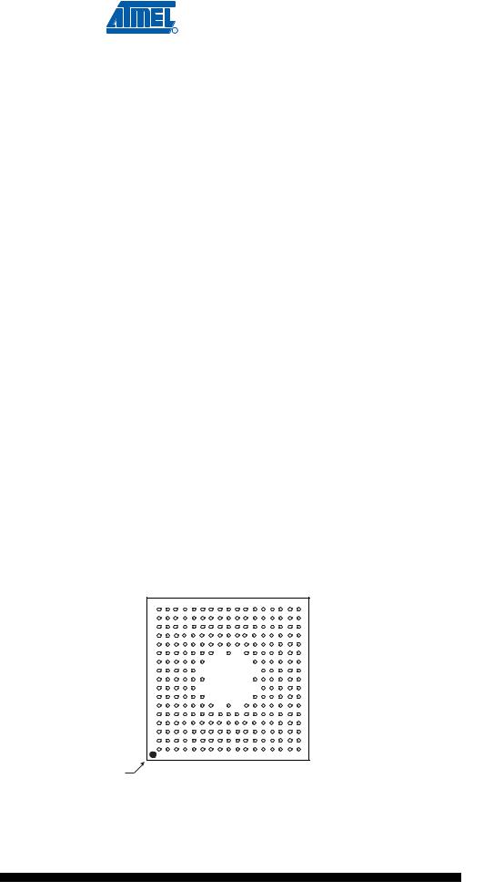
Table 4-1. |
|
|
|
|
|
|
|
|
|
|
|
|
|
|
|
|
|
|
|
|
|
|
|
|
|
|
|
|
|
AT91RM9200 Pinout for 208-pin PQFP Package (Continued) |
|
|
|
|
|
|||||||||
|
|
|
|
|
|
|
|
|
|
|
|
|
|
|
Pin |
|
|
Pin |
|
|
|
|
Pin |
|
|
Pin |
|
|
|
Number |
Signal Name |
|
Number |
Signal Name |
|
|
|
Number |
Signal Name |
|
Number |
Signal Name |
|
|
|
|
|
|
|
|
|
|
|
|
|
|
|
|
|
145 |
A11 |
|
161 |
PC7 |
|
|
|
177 |
|
CAS |
|
193 |
D10 |
|
146 |
VDDIOM |
|
162 |
PC8 |
|
|
|
178 |
|
SDWE |
|
194 |
D11 |
|
147 |
GND |
|
163 |
PC9 |
|
|
|
179 |
|
D0 |
|
195 |
D12 |
|
148 |
A12 |
|
164 |
VDDIOM |
|
|
|
180 |
|
D1 |
|
196 |
D13 |
|
149 |
A13 |
|
165 |
GND |
|
|
|
181 |
|
D2 |
|
197 |
D14 |
|
150 |
A14 |
|
166 |
NCS0/BFCS |
|
|
|
182 |
|
D3 |
|
198 |
D15 |
|
151 |
A15 |
|
167 |
NCS1/SDCS |
|
|
|
183 |
|
VDDIOM |
|
199 |
VDDIOM |
|
152 |
VDDCORE |
|
168 |
NCS2 |
|
|
|
184 |
|
GND |
|
200 |
GND |
|
153 |
GND |
|
169 |
NCS3/SMCS |
|
|
|
185 |
|
D4 |
|
201 |
PC16 |
|
154 |
A16/BA0 |
|
170 |
NRD/NOE/CFOE |
|
|
|
186 |
|
D5 |
|
202 |
PC17 |
|
155 |
A17/BA1 |
|
171 |
NWR0/NWE/CFWE |
|
|
|
187 |
|
D6 |
|
203 |
PC18 |
|
156 |
A18 |
|
172 |
NWR1/NBS1/CFIOR |
|
|
|
188 |
|
VDDCORE |
|
204 |
PC19 |
|
157 |
A19 |
|
173 |
NWR3/NBS3/CFIOW |
|
|
|
189 |
|
GND |
|
205 |
PC20 |
|
158 |
A20 |
|
174 |
SDCK |
|
|
|
190 |
|
D7 |
|
206 |
PC21 |
|
159 |
A21 |
|
175 |
SDCKE |
|
|
|
191 |
|
D8 |
|
207 |
PC22 |
|
160 |
A22 |
|
176 |
RAS |
|
|
|
192 |
|
D9 |
|
208 |
PC23 |
|
|
|
|
|
|
|
|
|
|
|
|
|
|
|
|
Note: 1. Shaded cells define the pins poweredMacshbM·by VDDIOM.
4.3256-ball BGA Package Outline
Figure 4-2 shows the orientation of the 256-ball LFBGA package.
A detailed mechanical description is given in the section “AT91RM9200 Mechanical Characteristics” of the product datasheet.
Figure 4-2. 256-ball LFBGA Package (Top View)
17
16
15
14
13
12
11
10
9
8
7
6
5
4
3
2
1
A B C D E F G H J K L M N P R T U
BALL A1
10 AT91RM9200
1768LS–ATARM–16-Jun-09
AT91RM9200
4.4256-ball BGA Package Pinout
Table 4-2. |
AT91RM9200 Pinout for 256-ball BGA Package |
|
|
|
|
|
|
|
||||
Pin |
|
Signal Name |
|
Pin |
Signal Name |
|
Pin |
Signal Name |
|
Pin |
Signal Name |
|
|
|
|
|
|
|
|
|
|
|
|
|
|
A1 |
|
TDI |
|
C3 |
PD14 |
|
E5 |
TCK |
|
G14 |
PA1 |
|
|
|
|
|
|
|
|
|
|
|
|
|
|
A2 |
|
JTAGSEL |
|
C4 |
PB22 |
|
E6 |
GND |
|
G15 |
PA2 |
|
|
|
|
|
|
|
|
|
|
|
|
|
|
A3 |
|
PB20 |
|
C5 |
PB19 |
|
E7 |
PB15 |
|
G16 |
PA3 |
|
|
|
|
|
|
|
|
|
|
|
|
|
|
A4 |
|
PB17 |
|
C6 |
PD10 |
|
E8 |
GND |
|
G17 |
XIN32 |
|
|
|
|
|
|
|
|
|
|
|
|
|
|
A5 |
|
PD11 |
|
C7 |
PB13 |
|
E9 |
PB7 |
|
H1 |
PD23 |
|
|
|
|
|
|
|
|
|
|
|
|
|
|
A6 |
|
PD8 |
|
C8 |
PB12 |
|
E10 |
PB3 |
|
H2 |
PD20 |
|
|
|
|
|
|
|
|
|
|
|
|
|
|
A7 |
|
VDDIOP |
|
C9 |
PB6 |
|
E11 |
PA29 |
|
H3 |
PD22 |
|
|
|
|
|
|
|
|
|
|
|
|
|
|
A8 |
|
PB9 |
|
C10 |
PB1 |
|
E12 |
PA26 |
|
H4 |
PD21 |
|
|
|
|
|
|
|
|
|
|
|
|
|
|
A9 |
|
PB4 |
|
C11 |
GND |
|
E13 |
PA25 |
|
H5 |
VDDIOP |
|
|
|
|
|
|
|
|
|
|
|
|
|
|
A10 |
|
PA31/BMS |
|
C12 |
PA20 |
|
E14 |
PA9 |
|
H13 |
VDDPLL |
|
|
|
|
|
|
|
|
|
|
|
|
|
|
A11 |
|
VDDIOP |
|
C13 |
PA18 |
|
E15 |
PA6 |
|
H14 |
VDDIOP |
|
|
|
|
|
|
|
|
|
|
|
|
|
|
A12 |
|
PA23 |
|
C14 |
VDDCORE |
|
E16 |
PD3 |
|
H15 |
GNDPLL |
|
|
|
|
|
|
|
|
|
|
|
|
|
|
A13 |
|
PA19 |
|
C15 |
GND |
|
E17 |
PD0 |
|
H16 |
GND |
|
|
|
|
|
|
|
|
|
|
|
|
|
|
A14 |
|
GND |
|
C16 |
PA8 |
|
F1 |
PD16 |
|
H17 |
XOUT32 |
|
|
|
|
|
|
|
|
|
|
|
|
|
|
A15 |
|
PA14 |
|
C17 |
PD5 |
|
F2 |
GND |
|
J1 |
PD25 |
|
|
|
|
|
|
|
|
|
|
|
|
|
|
A16 |
|
VDDIOP |
|
D1 |
TST1 |
|
F3 |
PB23 |
|
J2 |
PD27 |
|
|
|
|
|
|
|
|
|
|
|
|
|
|
A17 |
|
|
MacshbM· |
|
||||||||
|
PA13 |
|
D2 |
VDDIOP |
|
F4 |
PB25 |
|
J3 |
PD24 |
|
|
B1 |
|
TDO |
|
D3 |
VDDIOP |
|
F5 |
PB24 |
|
J4 |
PD26 |
|
B2 |
|
PD13 |
|
D4 |
GND |
|
F6 |
VDDCORE |
J5 |
PB28 |
|
|
|
|
|
|
|
|
|
|
|
|
|
|
|
B3 |
|
PB18 |
|
D5 |
VDDIOP |
|
F7 |
PB16 |
J6 |
PB29 |
|
|
|
|
|
|
|
|
|
|
|
|
|
|
|
B4 |
|
PB21 |
|
D6 |
PD7 |
|
F9 |
PB11 |
J12 |
GND |
|
|
|
|
|
|
|
|
|
|
|
|
|
|
|
B5 |
|
PD12 |
|
D7 |
PB14 |
|
F11 |
PA30 |
J13 |
GNDOSC |
|
|
|
|
|
|
|
|
|
|
|
|
|
|
|
B6 |
|
PD9 |
|
D8 |
VDDIOP |
|
F12 |
PA28 |
J14 |
VDDOSC |
|
|
|
|
|
|
|
|
|
|
|
|
|
|
|
B7 |
|
GND |
|
D9 |
PB8 |
|
F13 |
PA4 |
J15 |
VDDPLL |
|
|
|
|
|
|
|
|
|
|
|
|
|
|
|
B8 |
|
PB10 |
|
D10 |
PB2 |
|
F14 |
PD2 |
J16 |
GNDPLL |
|
|
|
|
|
|
|
|
|
|
|
|
|
|
|
B9 |
|
PB5 |
|
D11 |
GND |
|
F15 |
PD1 |
J17 |
XIN |
|
|
|
|
|
|
|
|
|
|
|
|
|
|
|
B10 |
|
PB0 |
|
D12 |
PA22 |
|
F16 |
PA5 |
K1 |
HDPA |
|
|
|
|
|
|
|
|
|
|
|
|
|
|
|
B11 |
|
VDDIOP |
|
D13 |
PA21 |
|
F17 |
PLLRCB |
K2 |
DDM |
|
|
|
|
|
|
|
|
|
|
|
|
|
|
|
B12 |
|
PA24 |
|
D14 |
PA16 |
|
G1 |
PD19 |
K3 |
HDMA |
|
|
|
|
|
|
|
|
|
|
|
|
|
|
|
B13 |
|
PA17 |
|
D15 |
PA10 |
|
G2 |
PD17 |
K4 |
VDDIOP |
|
|
|
|
|
|
|
|
|
|
|
|
|
|
|
B14 |
|
PA15 |
|
D16 |
PD6 |
|
G3 |
GND |
K5 |
DDP |
|
|
|
|
|
|
|
|
|
|
|
|
|
|
|
B15 |
|
PA11 |
|
D17 |
PD4 |
|
G4 |
PB26 |
K13 |
PC5 |
|
|
B16 |
|
PA12 |
|
E1 |
NRST |
|
G5 |
PD18 |
K14 |
PC4 |
|
|
B17 |
|
PA7 |
|
E2 |
NTRST |
|
G6 |
PB27 |
K15 |
PC6 |
|
|
C1 |
|
TMS |
|
E3 |
GND |
|
G12 |
PA27 |
|
K16 |
VDDIOM |
|
C2 |
|
PD15 |
|
E4 |
TST0 |
|
G13 |
PA0 |
|
K17 |
XOUT |
|
|
|
|
|
|
|
|
|
|
|
|
|
|
11
1768LS–ATARM–16-Jun-09

Table 4-2. AT91RM9200 Pinout for 256-ball BGA Package (Continued)
Pin |
|
Signal Name |
|
Pin |
|
Signal Name |
|
Pin |
Signal Name |
|
Pin |
Signal Name |
|
|
|
|
|
|
|
|
|
|
|
|
|
|
|
|
|
L1 |
|
GND |
|
|
N2 |
|
A5 |
|
P13 |
D15 |
|
T7 |
NWR1/NBS1/ |
|
|
|
|
|
|
|
CFIOR |
|
|||||||
|
|
|
|
|
|
|
|
|
|
|
|
|
|
|
L2 |
|
HDPB |
|
|
N3 |
|
A9 |
|
P14 |
PC26 |
|
T8 |
SDWE |
|
L3 |
|
HDMB |
|
|
N4 |
|
A4 |
|
P15 |
PC27 |
|
T9 |
GND |
|
L4 |
|
A6 |
|
|
N5 |
|
A14 |
|
P16 |
VDDIOM |
|
T10 |
VDDCORE |
|
L5 |
|
GND |
|
|
N6 |
|
SDA10 |
|
P17 |
GND |
|
T11 |
D9 |
|
L6 |
|
VDDIOP |
|
|
N7 |
|
A8 |
|
R1 |
GND |
|
T12 |
D12 |
|
L12 |
|
PC10 |
|
|
N8 |
|
A21 |
|
R2 |
GND |
|
T13 |
GND |
|
L13 |
|
PC15 |
|
|
N9 |
|
NRD/NOE/CFOE |
|
R3 |
A18 |
|
T14 |
PC19 |
|
L14 |
|
PC2 |
|
|
N10 |
|
RAS |
|
R4 |
A20 |
|
T15 |
PC21 |
|
L15 |
|
PC3 |
|
|
N11 |
|
D2 |
|
R5 |
PC8 |
|
T16 |
PC23 |
|
L16 |
|
VDDCORE |
|
N12 |
|
GND |
|
R6 |
VDDIOM |
|
T17 |
PC25 |
|
|
L17 |
|
PLLRCA |
|
|
N13 |
|
PC28 |
|
R7 |
NCS3/SMCS |
|
U1 |
VDDCORE |
|
|
|
|
|
|
|
|
|
|
|
|
|
|
|
|
M1 |
|
VDDIOM |
|
|
N14 |
|
PC31 |
|
R8 |
NWR3/NBS3/ |
|
U2 |
GND |
|
|
|
|
|
|
CFIOW |
|
|
|||||||
|
|
|
|
|
|
|
|
|
|
|
|
|
|
|
M2 |
|
GND |
|
|
N15 |
|
PC30 |
|
R9 |
D0 |
|
U3 |
A16/BA0 |
|
M3 |
|
A3 |
|
|
N16 |
|
PC11 |
|
R10 |
VDDIOM |
|
U4 |
A19 |
|
M4 |
|
A1/NBS2/NWR2 |
|
N17 |
|
PC12 |
|
R11 |
D8 |
|
U5 |
GND |
|
|
|
|
GND |
|
|
|
|
|
|
|
|
|
|
|
|
M7 |
|
P3 |
|
MacshbM·A12 R14 VDDIOM U8 CAS |
|
|||||||||
M5 |
|
A10 |
|
|
P1 |
|
A7 |
R12 |
D13 |
U6 |
NCS0/BFCS |
|
||
M6 |
|
A2 |
|
|
P2 |
|
A13 |
R13 |
PC17 |
U7 |
SDCK |
|
||
|
|
|
|
|
|
|
|
|
|
|
|
|
|
|
M9 |
|
NCS1/SDCS |
P4 |
|
VDDIOM |
R15 |
PC24 |
U9 |
D3 |
|
||||
M11 |
|
D4 |
|
|
P5 |
|
A11 |
|
R16 |
PC29 |
|
U10 |
D6 |
|
M12 |
|
GND |
|
|
P6 |
|
A22 |
|
R17 |
VDDIOM |
|
U11 |
D7 |
|
|
|
|
|
|
|
|
|
|
|
|
|
|
|
|
M13 |
|
PC13 |
|
|
P7 |
|
PC9 |
T1 |
A15 |
U12 |
D11 |
|
||
M14 |
|
PC1 |
|
|
P8 |
|
NWR0/NWE/CFWE |
|
T2 |
VDDCORE |
|
U13 |
D14 |
|
M15 |
|
PC0 |
|
|
P9 |
|
SDCKE |
|
T3 |
A17/BA1 |
|
U14 |
PC16 |
|
M16 |
|
GND |
|
|
P10 |
|
D1 |
|
T4 |
PC7 |
|
U15 |
PC18 |
|
M17 |
|
PC14 |
|
|
P11 |
|
D5 |
|
T5 |
VDDIOM |
|
U16 |
PC20 |
|
N1 |
|
A0/NBS0 |
|
|
P12 |
|
D10 |
|
T6 |
NCS2 |
|
U17 |
PC22 |
|
|
|
|
|
|
|
|
|
|
|
|
|
|
||
Note: |
1. Shaded cells define the balls powered by VDDIOM. |
|
|
|
|
|
|
|||||||
12 AT91RM9200 
1768LS–ATARM–16-Jun-09
Loading...