


U209B
U209B
Phase-Control IC ± Tacho Applications
Description
The integrated circuit U209B is designed as a phasecontrol circuit in bipolar technology with an internal frequency-voltage converter. Furthermore, it has an internal open-loop amplifier which means it can be used for motor speed control with tacho feedback.
The U209B is a 14-pin shrink version of the U211B with reduced features. Using the U209B, the designer is able to realize sophisticated as well as economic motor control systems.
Features
|
Internal frequency-to-voltage converter |
Triggering pulse typ. 155 mA |
|
|
Externally controlled integrated amplifier |
|
Internal supply-voltage monitoring |
|
Automatic soft start with minimized ªdead timeº |
|
Temperature-compensated reference source |
|
Voltage and current synchronization |
|
Current requirement ≤ 3 mA |
|
Retriggering |
|
|
Block Diagram
|
14(16) |
1(1) |
|
|
|
|
|
|
|
Voltage / Current |
Automatic |
|
Output |
4(4) |
|
||
|
|
|
|
|||||
|
detector |
|
retriggering |
|
pulse |
|
|
|
|
|
|
|
|
|
|
5(5) |
|
10(10) |
Control |
|
|
|
|
|
6(6) |
|
|
|
|
|
|
|
|
||
amplifier |
|
Phase |
|
|
|
|
|
|
|
|
|
|
|
|
|
||
|
+ |
|
|
|
|
3(3) |
±VS |
|
|
|
|
control unit |
|
Supply |
|||
9(9) |
|
|
|
|
||||
± |
|
= f (V |
) |
|
voltage |
2(2) |
|
|
|
|
11 |
|
|
limitation |
|
GND |
|
|
|
|
|
|
|
|
||
|
|
|
|
|
|
Reference |
|
|
|
|
|
|
|
|
voltage |
13(15) |
|
|
|
|
|
|
|
|
|
|
|
|
|
|
|
|
Voltage |
|
|
|
|
|
|
|
|
monitoring |
|
|
|
|
|
|
|
Frequency- |
|
|
|
|
|
|
Soft start |
|
to-voltage |
|
|
|
|
|
±VS |
|
|
converter |
U209B |
|
|
|
|
|
|
|
|
|
|
|
|
|
11(11) |
12(12) |
|
8(8) |
7(7) |
|
|
Figure 1. Block diagram (Pins in brackets refer to SO16)
Ordering Information
Extended Type Number |
Package |
Remarks |
U209B-x |
DIP14 |
Tube |
U209B-xFP |
SO16 |
Tube |
U209B-xFPG3 |
SO16 |
Taped and reeled |
Rev. A3, 11-Jan-01 |
1 (11) |

(11)2 |
|
|
|
|
|
|
|
|
|
|
|
|
|
|
IN4007 |
D 1 |
L |
U209B |
|
|
|
|
|
|
|
|
|
|
|
|
|
|
|
|
|
||||
|
|
|
|
|
|
|
|
|
|
|
|
|
|
|
|
18 k |
M |
|
|
|
|
|
|
|
|
|
|
|
|
|
|
|
|
|
|
2 W |
R 1 |
|
|
|
|
|
|
|
|
R 3 |
|
|
R4 |
|
|
|
|
|
|
|
|
|
|
|
|
|
|
|
220 k |
|
|
470 k |
|
|
|
|
|
|
|
|
|
|
|
|
R 9 |
|
|
|
14 |
|
|
1 |
|
|
|
|
|
|
|
TIC |
|
|
|
Figure |
47 k |
|
Set speed |
Voltage / Current |
Automatic |
|
Output |
|
|
|
236N |
230 V ~ |
|
||||||
|
|
|
|
|
|
|
|
|
|
|
|
|
|
4 |
|
R13 |
|
VM = |
|
|
|
|
|
|
|
|
|
|
|
|
|
|
|
|
|
|
|
||
.2 |
R12 |
|
voltage |
|
|
detector |
|
retriggering |
|
pulse |
|
220 |
|
|
|
||||
100 k |
|
|
|
|
|
|
|
|
|
|
|
|
|
||||||
Block |
|
|
|
|
|
|
|
|
|
|
|
|
|
||||||
|
|
|
|
|
|
|
|
|
|
|
|
|
|
|
|
|
|||
R10 |
R 11 |
|
|
|
|
|
|
|
|
|
5 |
R2 |
680 k |
|
|
|
|||
diagram |
10 |
|
Control |
|
|
|
|
|
|
|
|
|
|
|
|||||
56 k |
|
C 9 |
|
|
|
|
|
|
|
|
|
|
|
|
|
||||
|
|
100 k |
|
|
|
|
|
|
|
|
|
|
|
3.3 nF |
|
|
|
||
|
|
|
|
|
|
|
|
|
|
|
|
|
|
6 |
|
|
|
||
|
|
|
|
|
|
|
|
|
|
|
|
|
|
|
|
|
|
|
|
with |
|
|
|
|
|
+ |
amplifier |
|
Phase |
|
|
|
3 |
C 2 |
|
22 F |
|
|
|
typical |
|
|
2.2 F/16 V |
9 |
± |
|
|
control unit |
|
Supply |
2 |
±VS |
C 1 |
N |
|
||||
|
|
|
|
|
|
|
11 |
) |
|
limitation |
25 V |
|
|||||||
|
|
|
|
|
|
|
|
|
= f (V |
|
voltage |
|
|||||||
forcircuitry |
|
|
|
|
|
|
|
|
|
|
|
|
Reference |
|
GND |
C 10 |
2.2 F |
|
|
|
|
|
|
|
|
|
|
|
|
|
|
|
|
|
16 V |
|
|
||
|
|
|
|
|
|
|
|
|
|
|
|
|
|
|
|
|
|
||
|
|
|
|
|
|
|
|
|
|
|
|
|
voltage |
13 |
|
|
|
|
|
|
|
|
|
|
|
|
|
|
|
|
|
|
|
|
|
|
|
||
|
|
|
|
|
|
|
|
|
|
|
|
|
|
|
|
|
|
|
|
speed |
|
|
|
|
|
|
|
|
|
|
|
|
Voltage |
|
|
|
|
|
|
|
|
|
|
|
|
|
|
|
|
|
|
monitoring |
|
|
|
|
|
|
|
regulation |
|
|
|
|
|
|
|
|
|
|
|
|
|
|
|
|
|
|
|
|
|
|
|
|
|
|
|
|
|
|
converter |
|
|
|
|
|
|
|
|
|
|
|
|
|
|
|
|
|
|
|
|
Frequency |
U209B |
|
|
|
|
|
|
|
|
|
|
|
|
|
|
|
Soft start |
|
to voltage |
|
|
|
|
|
|
||
|
|
|
|
|
|
|
|
|
±Vs |
|
|
|
|
|
|
|
|
|
|
.Rev |
|
|
|
|
|
|
|
|
11 |
12 |
8 |
|
7 |
|
|
|
|
|
|
|
|
Actual |
|
R 8 |
|
|
|
|
|
|
220 nF |
|
|
|
|
|
|
||
|
|
|
|
|
|
|
|
|
|
|
|
|
|
|
|
|
|
||
A3, |
|
|
speed |
|
|
2 M |
C7 |
C 8 |
|
|
C 5 |
C 4 |
|
|
|
|
|
|
|
11 |
|
|
voltage |
C6 |
R6 |
|
2.2 F |
220 nF |
C 3 |
|
1 nF |
1 k |
|
|
|
|
|
|
|
|
|
|
|
|
16 V |
|
|
|
|
|
|
|
|||||||
- |
|
|
|
|
|
68 k |
|
|
R7 |
2.2 F |
|
|
|
|
Speed sensor |
|
|
|
|
-Jan |
|
|
|
|
100 nF |
|
|
|
|
R5 |
|
|
|
|
|||||
|
|
|
|
|
|
|
22 k |
16 V |
|
|
|
|
|
|
|
|
|||
|
|
|
|
|
|
|
|
|
|
|
|
|
|
|
|
|
|
|
|
01 |
|
|
|
|
|
|
|
|
|
|
|
|
|
|
|
|
|
|
|
U209B
Description
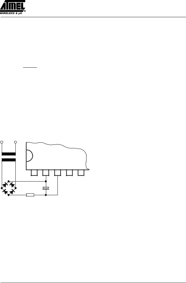
Mains Supply
The U209B is designed with voltage limiting and can therefore be supplied directly from the mains. The supply voltage between Pin 2 (+ pol/ ) and Pin 3 builds up across D1 and R1 and is smoothed by C1. The value of the series resistance can be approximated using:
R1 VM ± VS 2 IS
Further information regarding the design of the mains supply can be found in the chapter ªDesign Calculations for Mains Supplyº. The reference voltage source on Pin 13 of typ. ±8.9 V is derived from the supply voltage and represents the reference level of the control unit.
Operation using an externally stabilised DC voltage is not recommended.
If the supply cannot be taken directly from the mains because the power dissipation in R1 would be too large, then the circuit shown in the following figure 3 should be employed.
~ |
|
|
|
|
|
U209B |
|
|
|
24 V~ |
|
|
|
|
1 |
2 |
3 |
4 |
5 |
R1 |
C1 |
|
|
|
|
|
|
|
Figure 3. Supply voltage for high current requirements
Phase Control
The function of the phase control is largely identical to that of the well known integrated circuit U2008B. The phase angle of the trigger pulse is derived by comparing the ramp voltage. This is mains-synchronized by the voltage detector with the set value on the control input Pin 4. The slope of the ramp is determined by C2 and its charging current. The charging current can be varied using R2 on
Pin 5. The maximum phase angle can also be ad- max
justed using R2.
When the potential on Pin 6 reaches the nominal value predetermined at Pin 11, a trigger pulse is generated whose width tp is determined by the value of C2 (the value of C2 and hence the pulse width can be evaluated by assuming 8 s/nF).
The current sensor on Pin 1 ensures that no pulse is generated (for operation with inductive loads) in a new half cycle as long as the current from the previous half cycle is still flowing in the opposite direction to the supply voltage at that instant. This makes sure that ªGapsº in the load current are prevented.
The control signal on Pin 11 can be in the range 0 V to ±7 V (reference point Pin 2).
If V11 = ±7 V, the phase angle is at maximum = max, i.e., the current flow angle is a minimum. The minimum phase
angle is when V |
11 |
= V . |
min |
pin2 |
Voltage Monitoring
As the voltage is built up, uncontrolled output pulses are avoided by internal voltage surveillance. At the same time, all latches in the circuit (phase control, soft start) are reset and the soft-start capacitor is short circuited. Used with a switching hysteresis of 300 mV, this system guarantees defined start-up behaviour each time the supply voltage is switched on or after short interruptions of the mains supply.
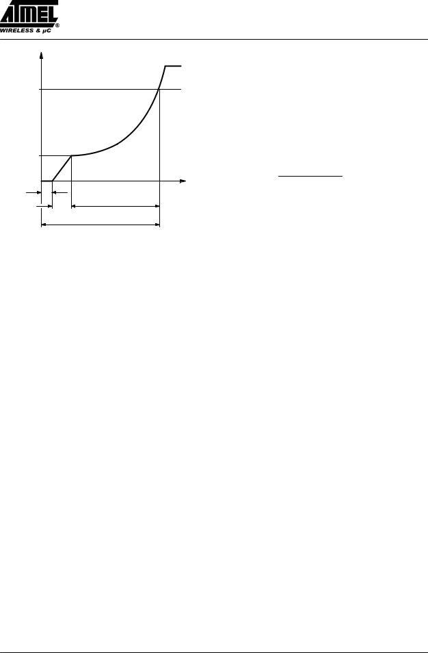
Soft Start
As soon as the supply voltage builds up (t1), the integrated soft start is initiated. Figure 4 shows the behaviour of the voltage across the soft-start capacitor which is identical with the voltage on the phase control input on Pin 11. This behaviour guarantees a gentle start-up for the motor and automatically ensures the optimum run-up time.
C3 is first charged up to the starting voltage Vo with typically 30 A current (t2). By then reducing the charging current to approx. 4 A, the slope of the charging function is substantially reduced so that the rotational speed of the motor only slowly increases. The charging current then increases as the voltage across C3 increases giving a progressively rising charging function which accelerates the motor with increasing rotational speed. The charging function determines the acceleration up to the set-point. The charging current can have a maximum value of 50 A.
Rev. A3, 11-Jan-01 |
3 (11) |
U209B |
|
|
|
|
VC3 |
|
|
The values of C5 and C6 must be such that for the highest |
|
|
|
possible input frequency, the maximum output voltage V0 |
||
|
|
|
does not exceed 6 V. The Ri on Pin 8 is approx. 6 kΩ while |
|
V12 |
|
|
C5 is charging up. To obtain good linearity of the |
|
|
|
|
f/V converter the time constant resulting from Ri and C5 |
|
|
|
|
should be considerably less (1/5) than the time span of the |
|
|
|
|
negative half cycle for the highest possible input |
|
|
|
|
frequency. The amount of remaining ripple on the output |
|
|
|
|
voltage on Pin 9 is dependent on C5, C6 and the internal |
|
V0 |
|
|
charge amplification. |
|
|
|
|
|
|
|
|
|
VO |
Gi Vch C5 |
|
|
|
t |
C6 |
t1 |
|
|
|
|
|
t3 |
|
|
|
t2 |
|
The ripple |
Vo can be reduced by using larger values of |
|
|
|
|||
|
ttot |
|
C6, however, the maximum conversion speed will then |
|
|
|
also be reduced. |
||
|
|
|
||
|
Figure 4. Soft start |
t1 |
= build-up of supply voltage |
t2 |
= charging of C3 to starting voltage |
t1 + t2 = dead time |
|
t3 |
= run-up time |
ttot |
= total start-up time to required speed |
Frequency-to-Voltage Converter
The internal frequency-to-voltage converter (f/V-converter) generates a DC signal on Pin 9 which is proportional to the rotational speed using an AC signal from a tacho generator or a light beam whose frequency is in turn dependent on the rotational speed. The high impedance input with a switch-on threshold of typ. ±100 mV gives very reliable operation even when relatively simple tacho generators are employed. The tacho frequency is given by:
|
n |
|
f = |
|
p[Hz] |
|
||
|
60 |
|
n = revolutions per minute |
|
|
p = number of pulses per revolution
The converter is based on the charge pumping principle. With each negative half wave of the input signal, a quantity of charge determined by C5 is internally amplified and then integrated by C6 at the converter output on Pin 9. The conversion constant is determined by C5, its charging voltage of Vch, R6 (Pin 9) and the internally adjusted charge amplification Gi.
k = Gi C5 R6 Vch
The analog output voltage is given by
|
Vo |
= k f |
where: |
Vch |
= 6.7 V |
|
Gi |
= 8.3 |
The value of this capacitor should be chosen to fit the particular control loop where it is going to be used.
Control Amplifier
The integrated control amplifier with differential input compares the set value (Pin 10) with the instantaneous value on Pin 9 and generates a regulating voltage on the output Pin 11 (together with external circuitry on Pin 12) which always tries to hold the real voltage at the value of the set voltages. The amplifier has a transmittance of typically 110 A/V and a bipolar current source output on Pin 11 which operates with typically ±100 A. The amplification and frequency response are determined by R7, C7, C8 and R8 (can be left out). For operation as a
power divider, C4, C5, R6, C6, R7, C7, C8 and R8 can be left out. Pin 9 should be connected with Pin 11 and Pin 7
with Pin 2. The phase angle of the triggering pulse can be adjusted using the voltage on Pin 10. An internal limiting circuit prevents the voltage on Pin 11 from becoming more negative than V13 + 1 V.
Pulse-Output Stage
The pulse-output stage is short-circuit protected and can typically deliver currents of 125 mA. For the design of smaller triggering currents, the function IGT = f (RGT) can be taken from figure 14.
Automatic Retriggering
The automatic retriggering prevents half cycles without current flow, even if the triacs are turned off earlier e.g., due to not exactly centered collector (brush lifter) or in the event of unsuccessful triggering. If necessary, another triggering pulse is generated after a time lapse of tPP = 4.5 tP and this is repeated until either the triac fires or the half cycle finishes.
4 (11) |
Rev. A3, 11-Jan-01 |
 Loading...