


 Loading...
BDTIC www.bdtic.com/ATMEL
Features
•Incorporates the ARM7TDMI ® ARM® Thumb® Processor
–High-performance 32-bit RISC Architecture
–High-density 16-bit Instruction Set
–Leader in MIPS/Watt
•EmbeddedICE™ In-circuit Emulation, Debug Communication Channel Support
•256 Kbytes of Internal High-speed Flash, Organized in 1024 Pages of 256 Bytes
–Single Cycle Access at Up to 30 MHz in Worst Case Conditions
–Prefetch Buffer Optimizing Thumb Instruction Execution at Maximum Speed
–Page Programming Time: 6 ms, Including Page Auto-erase, Full Erase Time: 15 ms
–10,000 Write Cycles, 10-year Data Retention Capability, Sector Lock Capabilities
•32K Bytes of Internal High-speed SRAM, Single-cycle Access at Maximum Speed
•Memory Controller (MC)
–Embedded Flash Controller, Abort Status and Misalignment Detection
–Memory Protection Unit
•Reset Controller (RSTC)
–Based on Three Power-on Reset Cells
–Provides External Reset Signal Shaping and Reset Sources Status
•Clock Generator (CKGR)
–Low-power RC Oscillator, 3 to 20 MHz On-chip Oscillator and One PLL
•Power Management Controller (PMC)
–Power Optimization Capabilities, including Slow Clock Mode (Down to 500 Hz), Idle Mode, Standby Mode and Backup Mode
–Four Programmable External Clock Signals
•Advanced Interrupt Controller (AIC)
–Individually Maskable, Eight-level Priority, Vectored Interrupt Sources
–Four External Interrupt Sources and One Fast Interrupt Source, Spurious Interrupt Protected
•Debug Unit (DBGU)
–2-wire UART and Support for Debug Communication Channel interrupt
•Periodic Interval Timer (PIT)
–20-bit Programmable Counter plus 12-bit Interval Counter
•Windowed Watchdog (WDT)
–12-bit key-protected Programmable Counter
–Provides Reset or Interrupt Signal to the System
–Counter May Be Stopped While the Processor is in Debug Mode or in Idle State
•Real-time Timer (RTT)
–32-bit Free-running Counter with Alarm
–Runs Off the Internal RC Oscillator
•Two Parallel Input/Output Controllers (PIO)
–Sixty-two Programmable I/O Lines Multiplexed with up to Two Peripheral I/Os
–Input Change Interrupt Capability on Each I/O Line
–Individually Programmable Open-drain, Pull-up resistor and Synchronous Output
•Shutdown Controller (SHDWC)
–Programmable Shutdown Pin and Wake-up Circuitry
•Two 32-bit Battery Backup Registers for a Total of 8 Bytes
•One 8-channel 20-bit PWM Controller (PWMC)
•One USB 2.0 Full Speed (12 Mbits per Second) Device Port
–On-chip Transceiver, 2376-byte Configurable Integrated FIFOs
AT91 ARM
Thumb-based
Microcontrollers
AT91SAM7A3
Preliminary
6042E–ATARM–14-Dec-06

•Nineteen Peripheral DMA Controller (PDC) Channels
•Two CAN 2.0B Active Controllers, Supporting 11-bit Standard and 29-bit Extended Identifiers
–16 Fully Programmable Message Object Mailboxes, 16-bit Time Stamp Counter
•Two 8-channel 10-bit Analog-to-Digital Converter
•Three Universal Synchronous/Asynchronous Receiver Transmitters (USART)
–Individual Baud Rate Generator, IrDA® Infrared Modulation/Demodulation
–Support for ISO7816 T0/T1 Smart Card, Hardware Handshaking, RS485 Support
•Two Master/Slave Serial Peripheral Interfaces (SPI)
–8- to 16-bit Programmable Data Length, Four External Peripheral Chip Selects
•Three 3-channel 16-bit Timer/Counters (TC)
–Three External Clock Inputs, Two Multi-purpose I/O Pins per Channel
–Double PWM Generation, Capture/Waveform Mode, Up/Down Capability
•Two Synchronous Serial Controllers (SSC)
–Independent Clock and Frame Sync Signals for Each Receiver and Transmitter
–I²S Analog Interface Support, Time Division Multiplex Support
–High-speed Continuous Data Stream Capabilities with 32-bit Data Transfer
•One Two-wire Interface (TWI)
–Master Mode Support Only, All Two-wire Atmel EEPROM’s Supported
•Multimedia Card Interface (MCI)
–Compliant with Multimedia Cards and SD Cards
–Automatic Protocol Control and Fast Automatic Data Transfers with PDC, MMC and SDCard Compliant
•IEEE® 1149.1 JTAG Boundary Scan on All Digital Pins
•Required Power Supplies
–Embedded 1.8V Regulator, Drawing up to 130 mA for the Core and the External Components, Enables 3.3V Single Supply Mode
–3.3V VDD3V3 Regulator, I/O Lines and Flash Power Supply
–1.8V VDD1V8 Output of the Voltage Regulator and Core Power Supply
–3V to 3.6V VDDANA ADC Power Supply
–3V to 3.6V VDDBU Backup Power Supply
•5V-tolerant I/Os
•Fully Static Operation: Up to 60 MHz at 1.65V and 85°C Worst Case Conditions
•Available in a 100-lead LQFP Green Package
2 AT91SAM7A3 Preliminary 
6042E–ATARM–14-Dec-06

AT91SAM7A3 Preliminary
1. Description
The AT91SAM7A3 is a member of a series of 32-bit ARM7™ microcontrollers with an integrated CAN controller. It features a 256-Kbyte high-speed Flash and 32-Kbyte SRAM, a large set of peripherals, including two 2.0B full CAN controllers, and a complete set of system functions minimizing the number of external components. The device is an ideal migration path for 8-bit microcontroller users looking for additional performance and extended memory.
The embedded Flash memory can be programmed in-system via the JTAG-ICE interface.
Built-in lock bits protect the firmware from accidental overwrite.
The AT91SAM7A3 integrates a complete set of features facilitating debug, including a JTAG Embedded ICE interface, misalignment detector, interrupt driven debug communication channel for user configurable trace on a console, and JTAG boundary scan for board level debug and test.
By combining a high-performance 32-bit RISC processor with a high-density 16-bit instruction set, Flash and SRAM memory, a wide range of peripherals including CAN controllers, 10-bit ADC, Timers and serial communication channels, on a monolithic chip, the AT91SAM7A3 is ideal for many compute-intensive embedded control applications.
3
6042E–ATARM–14-Dec-06

2. Block Diagram
Figure 2-1. AT91SAM7A3 Block Diagram
TDI |
|
|
|
|
|
|
|
TDO |
|
JTAG |
ICE |
ARM7TDMI |
|
|
|
TMS |
|
|
|
||||
|
SCAN |
Processor |
|
|
|||
TCK |
|
|
1.8 V |
|
|||
JTAGSEL |
|
|
|
|
|
VDD3V3 |
|
|
|
|
|
|
Voltage |
||
|
|
|
|
|
|
GND |
|
TST |
System Controller |
|
|
|
Regulator |
||
|
|
|
VDD1V8 |
||||
FIQ |
|
|
|
|
|
|
|
IRQ0-IRQ3 |
|
AIC |
|
|
|
|
|
|
|
|
|
|
Embedded |
|
|
DRXD |
PIO |
PDC |
|
FLASH |
|
Flash |
|
DBGU |
|
|
Controller |
|
|||
DTXD |
|
|
|
||||
|
|
PDC |
|
256K Bytes |
|
|
|
PCK0-PCK3 |
|
|
|
|
|
Memory |
|
|
|
|
|
|
Protection |
|
|
|
|
|
|
|
Memory |
|
|
PLLRC |
PLL |
PMC |
|
|
Unit |
|
|
|
|
Controller |
|
||||
XIN |
|
|
|
|
|
||
OSC |
|
|
SRAM |
|
Address |
|
|
XOUT |
|
|
|
|
|||
|
|
|
|
32K Bytes |
|
Decoder |
|
GND |
|
GPBR |
|
|
|
|
|
VDDBU |
RCOSC |
RTT |
|
Peripheral Bridge |
|
Abort |
|
|
|
|
|
||||
|
|
|
|
|
|
Status |
|
FWKUP |
|
Shutdown |
|
|
|
|
|
WKUP0 |
|
|
Peripheral Data |
|
|
|
|
|
Controller |
|
|
|
|
||
WKUP1 |
|
|
Controller |
Misalignment |
|
||
SHDW |
|
|
|
|
|||
|
|
|
19 channels |
|
Detection |
|
|
|
|
|
|
|
|
||
VDDBU |
POR |
|
|
|
|
|
|
|
|
|
|
|
|
|
|
NRST |
POR |
Reset |
|
APB |
FIFO |
Transceiver |
|
VDD3V3 |
Controller |
|
|
DDM |
|||
|
|
|
|
USB Device |
|
||
|
VDD1V8 POR |
|
|
|
|||
|
|
|
|
DDP |
|||
|
|
PIT |
|
|
TWI |
|
TWD |
|
|
|
|
|
|
||
|
|
WDT |
|
|
|
|
TWCK |
|
|
|
|
CAN0 |
|
CANRX0 |
|
|
|
|
|
|
|
CANTX0 |
|
|
PIOA |
PIOB |
|
|
CAN1 |
|
CANRX1 |
|
|
|
|
CANTX1 |
|||
|
|
|
|
|
|
|
|
|
|
|
|
|
|
|
PWM0 |
RXD0 |
|
PDC |
|
|
|
|
PWM1 |
|
|
|
|
|
PWM2 |
||
TXD0 |
|
|
|
|
|
|
|
|
USART0 |
|
|
PWMC |
|
PWM3 |
|
SCK0 |
|
|
|
|
|||
RTS0 |
|
|
|
|
|
|
PWM4 |
|
PDC |
|
|
|
|
PWM5 |
|
CTS0 |
|
|
|
|
|
||
|
PDC |
|
|
|
|
PWM6 |
|
RXD1 |
|
|
|
|
|
||
|
|
|
|
|
PWM7 |
||
TXD1 |
|
USART1 |
|
|
|
|
|
|
|
|
PDC |
|
TF0 |
||
SCK1 |
|
|
|
|
|||
|
|
|
|
SSC0 |
|
TK0 |
|
RTS1 |
|
|
|
|
|
||
|
PDC |
|
|
PIO |
TD0 |
||
CTS1 |
|
|
|
|
|||
|
|
|
|
|
RD0 |
||
RXD2 |
|
PDC |
|
|
|
||
TXD2 |
|
USART2 |
|
|
PDC |
|
RK0 |
|
|
|
|
RF0 |
|||
SCK2 |
|
|
|
|
|||
|
|
|
|
PDC |
|
TF1 |
|
RTS2 |
|
PDC |
|
|
|
||
CTS2 |
|
|
|
|
|
TK1 |
|
SPI0_NPCS0 |
|
PDC |
|
|
SSC1 |
|
TD1 |
SPI0_NPCS1 |
|
|
|
|
|
|
RD1 |
SPI0_NPCS2 |
|
SPI0 |
|
|
PDC |
|
RK1 |
SPI0_NPCS3 |
|
|
|
|
RF1 |
||
SPI0_MISO |
|
|
|
|
Timer Counter |
|
TCLK0 |
SPI0_MOSI |
|
|
|
|
|
||
|
PDC |
|
|
|
TCLK1 |
||
SPI0_SPCK |
|
|
|
|
|
TCLK2 |
|
SPI1_NPCS0 |
|
PDC |
|
|
|
|
|
|
|
|
TC0 |
|
TIOA0 |
||
SPI1_NPCS1 |
|
|
|
|
|||
|
|
|
|
|
TIOB0 |
||
SPI1_NPCS2 |
|
|
|
|
|
|
|
|
SPI1 |
|
|
|
|
TIOA1 |
|
SPI1_NPCS3 |
|
|
|
TC1 |
|
||
SPI1_MISO |
|
|
|
|
|
TIOB1 |
|
|
|
|
|
|
|
||
SPI1_MOSI |
|
|
|
|
TC2 |
|
TIOA2 |
SPI1_SPCK |
PIO |
PDC |
|
|
|
TIOB2 |
|
|
|
|
|
||||
MCCK |
PDC |
|
|
Timer Counter |
|
TCLK3 |
|
MCCDA |
|
MCI |
|
|
|
TCLK4 |
|
MCDA0-MCDA3 |
|
|
|
|
|
|
TCLK5 |
ADC0_AD0 |
|
PDC |
|
|
TC3 |
|
TIOA3 |
ADC0_AD1 |
|
|
|
|
|
TIOB3 |
|
ADC0_AD2 |
|
|
|
|
|
|
|
ADC0_AD3 |
|
|
|
|
TC4 |
|
TIOA4 |
ADC0_AD4 |
|
ADC0 |
|
|
|
TIOB4 |
|
ADC0_AD5 |
|
|
|
|
|
||
ADC0_AD6 |
|
|
|
|
|
|
TIOA5 |
ADC0_AD7 |
|
|
|
|
TC5 |
|
|
|
|
|
|
|
TIOB5 |
||
ADC0_ADTRG |
|
|
|
|
|
|
|
|
|
|
|
|
|
TCLK6 |
|
ADVREFP |
|
|
|
|
Timer Counter |
|
|
VDDANA |
|
PDC |
|
|
|
TCLK7 |
|
GND |
|
|
|
|
|
|
TCLK8 |
ADC1_AD0 |
|
|
|
|
TC6 |
|
TIOA6 |
ADC1_AD1 |
|
|
|
|
|
TIOB6 |
|
ADC1_AD2 |
|
ADC1 |
|
|
|
|
TIOA7 |
ADC1_AD3 |
|
|
|
TC7 |
|
||
ADC1_AD4 |
|
|
|
|
|
TIOB7 |
|
ADC1_AD5 |
|
|
|
|
|
|
TIOA8 |
ADC1_AD6 |
|
|
|
|
TC8 |
|
|
ADC1_AD7 |
|
|
|
|
|
TIOB8 |
|
ADC1_ADTRG |
|
|
|
|
|
|
|
4 AT91SAM7A3 Preliminary
6042E–ATARM–14-Dec-06

 AT91SAM7A3 Preliminary
3. Signal Description
Table 3-1. |
Signal Description |
|
|
|
|
|
|
|
|
Active |
|
Signal Name |
|
Function |
Type |
Level |
Comments |
|
|
|
|
|
|
|
|
Power |
|
|
|
|
|
|
|
|
|
VDD3V3 |
|
1.8V Voltage Regulator, I/O Lines and |
Power |
|
3.0V to 3.6V |
|
Flash Power Supply |
|
|||
|
|
|
|
|
|
|
|
|
|
|
|
VDDBU |
|
Backup I/O Lines Power Supply |
Power |
|
3V to 3.6V |
|
|
|
|
|
|
VDDANA |
|
Analog Power Supply |
Power |
|
3V to 3.6V |
|
|
|
|
|
|
VDD1V8 |
|
1.8V Voltage Regulator Output and Core |
Power |
|
1.85V typical |
|
Power Supply |
|
|||
|
|
|
|
|
|
|
|
|
|
|
|
VDDPLL |
|
1.8V PLL Power Supply |
Power |
|
1.65V to 1.95V |
|
|
|
|
|
|
GND |
|
Ground |
Ground |
|
|
|
|
|
|
|
|
|
|
Clocks, Oscillators and PLLs |
|
|
|
|
|
|
|
|
|
XIN |
|
Main Oscillator Input |
Input |
|
|
|
|
|
|
|
|
XOUT |
|
Main Oscillator Output |
Output |
|
|
|
|
|
|
|
|
PLLRC |
|
PLL Filter |
Input |
|
|
|
|
|
|
|
|
PCK0 - PCK3 |
|
Programmable Clock Output |
Output |
|
|
|
|
|
|
|
|
SHDW |
|
Shut-Down Control |
Output |
|
Open Drain. |
|
|
|
|
|
|
WKUP0 - WKUP1 |
Wake-Up Inputs |
Input |
|
Accept between 0V and VDDBU |
|
|
|
|
|
|
|
FWKUP |
|
Force Wake Up |
Input |
|
Accept between 0V and VDDBU |
|
|
External pull-up resistor needed. |
|||
|
|
|
|
|
|
|
|
|
|
|
|
|
|
ICE and JTAG |
|
|
|
|
|
|
|
|
|
TCK |
|
Test Clock |
Input |
|
No pull-up resistor |
|
|
|
|
|
|
TDI |
|
Test Data In |
Input |
|
No pull-up resistor |
|
|
|
|
|
|
TDO |
|
Test Data Out |
Output |
|
|
|
|
|
|
|
|
TMS |
|
Test Mode Select |
Input |
|
No pull-up resistor |
|
|
|
|
|
|
JTAGSEL |
|
JTAG Selection |
Input |
|
Pull-down resistor |
|
|
|
|
|
|
|
|
Reset/Test |
|
|
|
|
|
|
|
|
|
NRST |
|
Microcontroller Reset |
I/O |
Low |
|
|
|
|
|
|
|
TST |
|
Test Mode Select |
Input |
High |
Pull-down resistor |
|
|
|
|
|
|
|
|
Debug Unit |
|
|
|
|
|
|
|
|
|
DRXD |
|
Debug Receive Data |
Input |
|
|
|
|
|
|
|
|
DTXD |
|
Debug Transmit Data |
Output |
|
|
|
|
|
|
|
|
5
6042E–ATARM–14-Dec-06

Table 3-1. |
|
|
|
|
|
|
|
|
|
|
|
|
|
|
|
|
|
|
|
Signal Description (Continued) |
|
|
|
|
|||||
|
|
|
|
|
|
|
|
|
|
|
|
|
|
|
|
|
|
Active |
|
Signal Name |
|
Function |
Type |
Level |
Comments |
||||
|
|
|
|
|
|
|
|||
|
|
AIC |
|
|
|
|
|||
|
|
|
|
|
|
|
|||
IRQ0 - IRQ3 |
|
External Interrupt Inputs |
|
Input |
|
|
|||
|
|
|
|
|
|
|
|||
FIQ |
|
Fast Interrupt Input |
|
Input |
|
|
|||
|
|
|
|
|
|
|
|||
|
|
PIO |
|
|
|
|
|||
|
|
|
|
|
|
|
|||
PA0 - PA31 |
|
Parallel IO Controller A |
|
I/O |
|
Pulled-up input at reset |
|||
|
|
|
|
|
|
|
|||
PB0 - PB29 |
|
Parallel IO Controller B |
|
I/O |
|
Pulled-up input at reset |
|||
|
|
|
|
|
|
||||
|
|
Multimedia Card Interface |
|
|
|||||
|
|
|
|
|
|
||||
MCCK |
|
Multimedia Card Clock |
Output |
|
|
||||
|
|
|
|
|
|
|
|||
MCCDA |
|
Multimedia Card A Command |
|
I/O |
|
|
|||
|
|
|
|
|
|
||||
MCDA0 - MCDA3 |
Multimedia Card A Data |
|
I/O |
|
|
||||
|
|
|
|
|
|
|
|||
|
|
USB Device Port |
|
|
|
|
|||
|
|
|
|
|
|
||||
DDM |
|
USB Device Port Data - |
Analog |
|
|
||||
|
|
|
|
|
|
||||
DDP |
|
USB Device Port Data + |
Analog |
|
|
||||
|
|
|
|
|
|
|
|||
|
|
USART |
|
|
|
|
|||
|
|
|
|
|
|
||||
SCK0 - SCK1 - SCK2 |
Serial Clock |
|
I/O |
|
|
||||
|
|
|
|
|
|
||||
TXD0 - TXD1 - TXD2 |
Transmit Data |
|
I/O |
|
|
||||
|
|
|
|
|
|
||||
RXD0 - RXD1 - RXD2 |
Receive Data |
|
Input |
|
|
||||
|
|
|
|
|
|||||
RTS0 - RTS1 - RTS2 |
Request To Send |
Output |
|
|
|||||
|
|
|
|
|
|
||||
CTS0 - CTS1 - CTS2 |
Clear To Send |
|
Input |
|
|
||||
|
|
|
|
|
|
||||
|
|
Synchronous Serial Controller |
|
|
|||||
|
|
|
|
|
|
||||
TD0 - TD1 |
|
Transmit Data |
Output |
|
|
||||
|
|
|
|
|
|
|
|||
RD0 - RD1 |
|
Receive Data |
|
Input |
|
|
|||
|
|
|
|
|
|
|
|||
TK0 - TK1 |
|
Transmit Clock |
|
I/O |
|
|
|||
|
|
|
|
|
|
|
|||
RK0 - RK1 |
|
Receive Clock |
|
I/O |
|
|
|||
|
|
|
|
|
|
|
|||
TF0 - TF1 |
|
Transmit Frame Sync |
|
I/O |
|
|
|||
|
|
|
|
|
|
|
|||
RF0 - RF1 |
|
Receive Frame Sync |
|
I/O |
|
|
|||
|
|
|
|
|
|
|
|||
|
|
Timer/Counter |
|
|
|
|
|||
|
|
|
|
|
|
||||
TCLK0 - TCLK8 |
External Clock Input |
|
Input |
|
|
||||
|
|
|
|
|
|
||||
TIOA0 - TIOA8 |
I/O Line A |
|
I/O |
|
|
||||
|
|
|
|
|
|
||||
TIOB0 - TIOB8 |
I/O Line B |
|
I/O |
|
|
||||
|
|
|
|
|
|
|
|||
|
|
PWM Controller |
|
|
|
|
|||
|
|
|
|
|
|||||
PWM0 - PWM7 |
PWM Channels |
Output |
|
|
|||||
|
|
|
|
|
|
|
|
|
|
6 AT91SAM7A3 Preliminary 
6042E–ATARM–14-Dec-06

 AT91SAM7A3 Preliminary
Table 3-1. |
Signal Description (Continued) |
|
|
|
||
|
|
|
|
|
Active |
|
Signal Name |
|
Function |
|
Type |
Level |
Comments |
|
|
|
|
|
|
|
|
|
SPI |
|
|
|
|
|
|
|
|
|
|
|
SPI0_MISO |
|
Master In Slave Out |
|
I/O |
|
|
SPI1_MISO |
|
|
|
|
||
|
|
|
|
|
|
|
|
|
|
|
|
|
|
SPI0_MOSI |
|
Master Out Slave In |
|
I/O |
|
|
SPI1_MOSI |
|
|
|
|
||
|
|
|
|
|
|
|
|
|
|
|
|
|
|
SPI0_SPCK |
|
SPI Serial Clock |
|
I/O |
|
|
SPI1_SPCK |
|
|
|
|
||
|
|
|
|
|
|
|
|
|
|
|
|
|
|
SPI0_NPCS0 |
|
SPI Peripheral Chip Select 0 |
|
I/O |
Low |
|
SPI1_NPCS0 |
|
|
|
|||
|
|
|
|
|
|
|
|
|
|
|
|
|
|
SPI0_NPCS1 - SPI0_NPCS3 |
SPI Peripheral Chip Select |
|
Output |
Low |
|
|
SPI1_NPCS1 - SPI1_NPCS3 |
|
|
||||
|
|
|
|
|
||
|
|
|
|
|
|
|
|
|
Two-wire Interface |
|
|
|
|
|
|
|
|
|
|
|
TWD |
|
Two-wire Serial Data |
|
I/O |
|
|
|
|
|
|
|
|
|
TWCK |
|
Two-wire Serial Clock |
|
I/O |
|
|
|
|
|
|
|
|
|
|
|
Analog-to-Digital Converter |
|
|
||
|
|
|
|
|
|
|
ADC0_AD0 - ADC0_AD7 |
Analog Inputs |
|
Analog |
|
Digital pulled-up inputs at reset |
|
ADC1_AD0 - ADC1_AD7 |
|
|
||||
|
|
|
|
|
||
|
|
|
|
|
|
|
ADVREFP |
|
Analog Positive Reference |
|
Analog |
|
|
|
|
|
|
|
|
|
ADC0_ADTRG |
ADC Trigger |
|
Input |
|
|
|
ADC1_ADTRG |
|
|
|
|||
|
|
|
|
|
||
|
|
|
|
|
|
|
|
|
CAN Controller |
|
|
|
|
|
|
|
|
|
|
|
CANRX0-CANRX1 |
CAN Inputs |
|
Input |
|
|
|
|
|
|
|
|
|
|
CANTX0-CANTX1 |
CAN Outputs |
|
Output |
|
|
|
|
|
|
|
|
|
|
7
6042E–ATARM–14-Dec-06

4. Package
4.1100-lead LQFP Package Outline
Figure 4-1 shows the orientation of the 100-lead LQFP package. A detailed mechanical description is given in the Mechanical Characteristics section of the full datasheet.
Figure 4-1. 100-lead LQFP Outline (Top View)
75 |
51 |
76 |
50 |
100
26
1 |
25 |
8 AT91SAM7A3 Preliminary 
6042E–ATARM–14-Dec-06

AT91SAM7A3 Preliminary
4.2Pinout
Table 4-1. |
Pinout in 100-lead LQFP Package |
|
|
|
|
|
|
||||
1 |
|
GND |
|
26 |
VDDBU |
|
51 |
PA20 |
|
76 |
PLLRC |
|
|
|
|
|
|
|
|
|
|
|
|
2 |
|
NRST |
|
27 |
FWKUP |
|
52 |
PA21 |
|
77 |
VDDANA |
|
|
|
|
|
|
|
|
|
|
|
|
3 |
|
TST |
|
28 |
WKUP0 |
|
53 |
PA22 |
|
78 |
ADVREFP |
|
|
|
|
|
|
|
|
|
|
|
|
4 |
|
PB13 |
|
29 |
WKUP1 |
|
54 |
PA23 |
|
79 |
GND |
|
|
|
|
|
|
|
|
|
|
|
|
5 |
|
PB12 |
|
30 |
SHDW |
|
55 |
PA24 |
|
80 |
PB14/ADC0_AD0 |
|
|
|
|
|
|
|
|
|
|
|
|
6 |
|
PB11 |
|
31 |
GND |
|
56 |
PA25 |
|
81 |
PB15/ADC0_AD1 |
|
|
|
|
|
|
|
|
|
|
|
|
7 |
|
PB10 |
|
32 |
PA4 |
|
57 |
PA26 |
|
82 |
PB16/ADC0_AD2 |
|
|
|
|
|
|
|
|
|
|
|
|
8 |
|
PB9 |
|
33 |
PA5 |
|
58 |
PA27 |
|
83 |
PB17/ADC0_AD3 |
|
|
|
|
|
|
|
|
|
|
|
|
9 |
|
PB8 |
|
34 |
PA6 |
|
59 |
VDD1V8 |
|
84 |
PB18/ADC0_AD4 |
|
|
|
|
|
|
|
|
|
|
|
|
10 |
|
PB7 |
|
35 |
PA7 |
|
60 |
GND |
|
85 |
PB19/ADC0_AD5 |
|
|
|
|
|
|
|
|
|
|
|
|
11 |
|
PB6 |
|
36 |
PA8 |
|
61 |
VDD3V3 |
|
86 |
PB20/ADC0_AD6 |
|
|
|
|
|
|
|
|
|
|
|
|
12 |
|
PB5 |
|
37 |
PA9 |
|
62 |
PA28 |
|
87 |
PB21/ADC0_AD7 |
|
|
|
|
|
|
|
|
|
|
|
|
13 |
|
PB4 |
|
38 |
VDD3V3 |
|
63 |
PA29 |
|
88 |
VDD3V3 |
|
|
|
|
|
|
|
|
|
|
|
|
14 |
|
PB3 |
|
39 |
GND |
|
64 |
PA30 |
|
89 |
PB22/ADC1_AD0 |
|
|
|
|
|
|
|
|
|
|
|
|
15 |
|
VDD3V3 |
|
40 |
VDD1V8 |
|
65 |
PA31 |
|
90 |
PB23/ADC1_AD1 |
|
|
|
|
|
|
|
|
|
|
|
|
16 |
|
GND |
|
41 |
PA10 |
|
66 |
JTAGSEL |
|
91 |
PB24/ADC1_AD2 |
|
|
|
|
|
|
|
|
|
|
|
|
17 |
|
VDD1V8 |
|
42 |
PA11 |
|
67 |
TDI |
|
92 |
PB25/ADC1_AD3 |
|
|
|
|
|
|
|
|
|
|
|
|
18 |
|
PB2 |
|
43 |
PA12 |
|
68 |
TMS |
|
93 |
PB26/ADC1_AD4 |
|
|
|
|
|
|
|
|
|
|
|
|
19 |
|
PB1 |
|
44 |
PA13 |
|
69 |
TCK |
|
94 |
PB27/ADC1_AD5 |
|
|
|
|
|
|
|
|
|
|
|
|
20 |
|
PB0 |
|
45 |
PA14 |
|
70 |
TDO |
|
95 |
PB28/ADC1_AD6 |
|
|
|
|
|
|
|
|
|
|
|
|
21 |
|
PA0 |
|
46 |
PA15 |
|
71 |
GND |
|
96 |
PB29/ADC1_AD7 |
|
|
|
|
|
|
|
|
|
|
|
|
22 |
|
PA1 |
|
47 |
PA16 |
|
72 |
VDDPLL |
|
97 |
DDM |
|
|
|
|
|
|
|
|
|
|
|
|
23 |
|
PA2 |
|
48 |
PA17 |
|
73 |
XOUT |
|
98 |
DDP |
|
|
|
|
|
|
|
|
|
|
|
|
24 |
|
PA3 |
|
49 |
PA18 |
|
74 |
XIN |
|
99 |
VDD1V8 |
|
|
|
|
|
|
|
|
|
|
|
|
25 |
|
GND |
|
50 |
PA19 |
|
75 |
GND |
|
100 |
VDD3V3 |
|
|
|
|
|
|
|
|
|
|
|
|
9
6042E–ATARM–14-Dec-06

5. Power Considerations
5.1Power Supplies
The AT91SAM7A3 has five types of power supply pins:
•VDD3V3 pins. They power the voltage regulator, the I/O lines, the Flash and the USB transceivers; voltage ranges from 3.0V to 3.6V, 3.3V nominal.
•VDD1V8 pins. They are the outputs of the 1.8V voltage regulator and they power the logic of the device.
•VDDPLL pin. It powers the PLL; voltage ranges from 1.65V to 1.95V, 1.8V typical. They can be connected to the VDD1V8 pin with decoupling capacitor.
•VDDBU pin. It powers the Slow Clock oscillator and the Real Time Clock, as well as a part of the System Controller; ranges from 3.0V and 3.6V, 3.3V nominal.
•VDDANA pin. It powers the ADC; ranges from 3.0V and 3.6V, 3.3V nominal.
No separate ground pins are provided for the different power supplies. Only GND pins are provided and should be connected as shortly as possible to the system ground plane.
5.2Voltage Regulator
The AT91SAM7A3 embeds a voltage regulator that consumes less than 120 µA static current and draws up to 130 mA of output current.
Adequate output supply decoupling is mandatory for VDD1V8 (pin 99)to reduce ripple and avoid oscillations. The best way to achieve this is to use two capacitors in parallel: one external 470 pF (or 1 nF) NPO capacitor must be connected between VDD1V8 and GND as close to the chip as possible. One external 3.3 µF (or 4.7 µF) X7R capacitor must be connected between VDD1V8 and GND.
All other VDD1V8 pins must be externally connected and have a proper decoupling capacitor (at least 100 nF).
Adequate input supply decoupling is mandatory for VDD3V3 (pin 100) in order to improve startup stability and reduce source voltage drop. The input decoupling capacitor should be placed close to the chip. For example, two capacitors can be used in parallel: 100 nF NPO and 4.7 µF X7R.
All other VDD3V3 pins must be externally connected and have a proper decoupling capacitor (at least 100 nF).
10 AT91SAM7A3 Preliminary 
6042E–ATARM–14-Dec-06
AT91SAM7A3 Preliminary
5.3Typical Powering Schematics
5.3.13.3V Single Supply
The AT91SAM7A3 supports a 3.3V single supply mode. The internal regulator is connected to the 3.3V source and its output feeds VDDPLL. Figure 5-1 shows the power schematics to be used for USB bus-powered systems.
Figure 5-1. 3.3V System Single Power Supply Schematics
USB Connector
up to 5.5V
|
VDDBU |
DC/DC Converter |
VDDANA |
|
|
VDD3V3 |
|
3.3V |
Voltage |
|
Regulator |
||
|
VDD1V8 |
VDDPLL |
11
6042E–ATARM–14-Dec-06

6. I/O Lines Considerations
6.1JTAG Port Pins
TMS, TDI and TCK are schmitt trigger inputs. TMS and TCK are 5V-tolerant, TDI is not. TMS,
TDI and TCK do not integrate any resistors and have to be pulled-up externally.
TDO is an output, driven at up to VDD3V3.
The JTAGSEL pin is used to select the JTAG boundary scan when asserted at a high level.
The JTAGSEL pin integrates a permanent pull-down resistor so that it can be left unconnected for normal operations.
6.2Test Pin
The TST pin is used for manufacturing tests and integrates a pull-down resistor so that it can be left unconnected for normal operations. Driving this line at a high level leads to unpredictable results.
6.3Reset Pin
The NRST pin is bidirectional. It is handled by the on-chip reset controller and can be driven low to provide a reset signal to the external components or asserted low externally to reset the microcontroller. There is no constraint on the length of the reset pulse, and the reset controller can guarantee a minimum pulse length. This allows connection of a simple push-button on the NRST pin as system user reset, and the use of the NRST signal to reset all the components of the system.
6.4PIO Controller A and B Lines
All the I/O lines PA0 to PA31 and PB0 to PB29 are 5V-tolerant and all integrate a programmable pull-up resistor. Programming of this pull-up resistor is performed independently for each I/O line through the PIO Controllers.
5V-tolerant means that the I/O lines can drive voltage level according to VDD3V3, but can be driven with a voltage at up to 5.5V. However, driving an I/O line with a voltage over VDD3V3 while the programmable pull-up resistor is enabled creates a current path through the pull-up resistor from the I/O line to VDDIO. Care should be taken, especially at reset, as all the I/O lines default as inputs with pull-up resistor enabled at reset.
6.5Shutdown Logic Pins
The SHDW pin is an open drain output. It can be tied to VDDBU with an external pull-up resistor.
The FWUP, WKUP0 and WKUP1 pins are input-only. They can accept voltages only between 0V and VDDBU. It is recommended to tie these pins either to GND or to VDDBU with an external resistor.
6.6I/O Line Drive Levels
All the I/O lines can draw up to 2 mA.
12 AT91SAM7A3 Preliminary 
6042E–ATARM–14-Dec-06

AT91SAM7A3 Preliminary
7. Processor and Architecture
7.1ARM7TDMI Processor
•RISC Processor Based on ARMv4T Von Neumann Architecture
–Runs at up to 60 MHz, providing 0.9 MIPS/MHz
•Two instruction sets
–ARM high-performance 32-bit Instruction Set
–Thumb high code density 16-bit Instruction Set
•Three-stage pipeline architecture
–Instruction Fetch (F)
–Instruction Decode (D)
–Execute (E)
7.2Debug and Test Features
•Integrated EmbeddedICE™ (embedded in-circuit emulator)
–Two watchpoint units
–Test access port accessible through a JTAG protocol
–Debug communication channel
•Debug Unit
–Two-pin UART
–Debug communication channel interrupt handling
–Chip ID Register
•IEEE1149.1 JTAG Boundary-scan on all digital pins
7.3Memory Controller
•Bus Arbiter
–Handles requests from the ARM7TDMI and the Peripheral Data Controller
•Address Decoder Provides Selection Signals for
–Three internal 1Mbyte memory areas
–One 256 Mbyte embedded peripheral area
•Abort Status Registers
–Source, Type and all parameters of the access leading to an abort are saved
–Facilitates debug by detection of bad pointers
•Misalignment Detector
–Alignment checking of all data accesses
–Abort generation in case of misalignment
•Remap Command
–Remaps the Internal SRAM in place of the embedded non-volatile memory
–Allows handling of dynamic exception vectors
•16-area Memory Protection Unit
–Individually programmable size between 1K Bytes and 1M Bytes
13
6042E–ATARM–14-Dec-06

–Individually programmable protection against write and/or user access
–Peripheral protection against write and/or user access
•Embedded Flash Controller
–Embedded Flash interface, up to three programmable wait states
–Read-optimized interface, buffering and anticipating the 16-bit requests, reducing the required wait states
–Password-protected program, erase and lock/unlock sequencer
–Automatic consecutive programming, erasing and locking operations
–Interrupt generation in case of forbidden operation
7.4Peripheral DMA Controller
•Handles data transfer between peripherals and memories
•Nineteen Channels
–Two for each USART
–Two for the Debug Unit
–Two for each Serial Synchronous Controller
–Two for each Serial Peripheral Interface
–One for the Multimedia Card Interface
–One for each Analog-to-Digital Converter
•Low bus arbitration overhead
–One Master Clock cycle needed for a transfer from memory to peripheral
–Two Master Clock cycles needed for a transfer from peripheral to memory
•Next Pointer management for reducing interrupt latency requirements
14 AT91SAM7A3 Preliminary 
6042E–ATARM–14-Dec-06

AT91SAM7A3 Preliminary
8. Memory
8.1Embedded Memories
•256 Kbytes of Flash Memory
–1024 pages of 256 bytes.
–Fast access time, 30 MHz single cycle access in worst case conditions.
–Page programming time: 6 ms, including page auto-erase
–Full erase time: 15 ms
–10,000 write cycles, 10-year data retention capability
–16 lock bits, each protecting 16 pages
•32 Kbytes of Fast SRAM
–Single-cycle access at full speed
15
6042E–ATARM–14-Dec-06
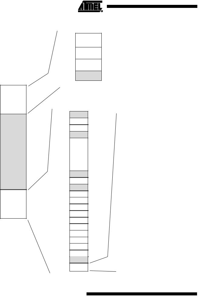
Figure 8-1. AT91SAM7A3 Memory Mapping
Internal Memory Mapping
0x0000 0000
Flash before Remap
SRAM after Remap
0x000F FFF 0x0010 0000
Internal Flash
0x001F FFF 0x0020 0000
Internal SRAM
0x002F FFF
0x0030 0000
Reserved
0x0FFF FFFF
Address Memory Space
0x0000 0000
Internal Memories |
256 MBytes |
|
|
Peripheral Mapping |
|
0x0FFF FFFF |
0xF000 0000 |
Reserved |
|
0x1000 0000 |
0xFFF7 FFFF |
|
|
|
|
||
|
0xFFF8 0000 |
CAN0 |
16 Kbytes |
|
|
0xFFF8 3FFF |
|
|
0xFFF8 4000 |
CAN1 |
16 Kbytes |
|
0xFFF8 7FFF |
|
|
0xFFF8 8000 |
Reserved |
|
0xFFF9 FFFF |
|
|
|
|
|
0xFFFA 0000 |
TC0, TC1, TC2 |
16 Kbytes |
|
|
|
0xFFFA 3FFF |
|
|
|
Undefined |
14 x 256 MBytes |
0xFFFA 4000 |
TC3, TC4, TC5 |
16 Kbytes |
|
0xFFFA 7FFF |
|||||
|
|
||||
(Abort) |
3,584 MBytes |
0xFFFA 8000 |
TC6, TC7, TC8 |
16 Kbytes |
|
|
|
0xFFFA BFFF |
|||
|
|
|
|
||
|
|
0xFFFA C000 |
MCI |
16 Kbytes |
|
|
|
0xFFFA FFFF |
|||
|
|
|
|
||
|
|
0xFFFB 0000 |
UDP |
16 Kbytes |
|
|
|
|
|
|
0xFFFB 3FFF |
|
|
|
|
0xFFFB 4000 |
Reserved |
|
|
|
0xFFFB 7FFF |
|
|
|
|
|
|
|
|
|
0xFFFB 8000 |
TWI |
16 Kbytes |
|
|
0xFFFB BFFF |
||
|
|
|
|
|
0xEFFF FFFF |
|
0xFFFB C000 |
Reserved |
|
|
0xFFFB FFFF |
|
||
|
|
|
||
0xF000 0000 |
|
|
|
|
|
0xFFFC 0000 |
USART0 |
16 Kbytes |
|
|
|
0xFFFC 3FFF |
||
|
|
|
|
|
|
|
0xFFFC 4000 |
USART1 |
16 Kbytes |
|
|
0xFFFC 7FFF |
||
Internal Peripherals |
256 MBytes |
|
|
|
0xFFFC 8000 |
|
|
||
|
|
USART2 |
16 Kbytes |
|
|
|
0xFFFC BFFF |
||
|
|
|
|
|
|
|
0xFFFC C000 |
PWMC |
16 Kbytes |
0xFFFF FFFF |
|
0xFFFC FFFF |
||
|
|
|
||
|
|
0xFFFD 0000 |
SSC0 |
16 Kbytes |
|
|
0xFFFD 3FFF |
||
|
|
|
|
|
|
|
0xFFFD 4000 |
SSC1 |
16 Kbytes |
|
|
0xFFFD 7FFF |
||
|
|
|
|
|
|
|
0xFFFD 8000 |
ADC0 |
16 Kbytes |
|
|
0xFFFD BFFF |
||
|
|
|
|
|
|
|
0xFFFD C000 |
ADC1 |
16 Kbytes |
|
|
0xFFFD FFFF |
||
|
|
|
|
|
|
|
0xFFFE 0000 |
SPI0 |
16 Kbytes |
|
|
0xFFFE 3FFF |
||
|
|
|
|
|
|
|
0xFFFE 4000 |
SPI1 |
16 Kbytes |
|
|
0xFFFE 7FFF |
||
|
|
|
|
|
|
|
0xFFFE 8000 |
Reserved |
|
|
|
0xFFFF EFFF |
|
|
|
|
|
|
|
|
|
0xFFFF F000 |
SYSC |
|
|
|
|
|
|
|
|
0xFFFF FFFF |
|
|
1 MBytes
1 MBytes
1 MBytes
252 MBytes
System Controller Mapping
0xFFFF F000 |
|
|
|
|
AIC |
512 Bytes/128 registers |
|
0xFFFF F1FF |
|
|
|
0xFFFF F200 |
|
|
|
|
DBGU |
512 Bytes/128 registers |
|
0xFFFF F3FF |
|
|
|
0xFFFF F400 |
|
|
|
|
PIOA |
512 Bytes/128 registers |
|
0xFFFF F5FF |
|
|
|
0xFFFF F600 |
|
|
|
|
PIOB |
512 Bytes/128 registers |
|
0xFFFF F7FF |
|
|
|
0xFFFF F800 |
Reserved |
|
|
|
|
||
0xFFFF FBFF |
|
|
|
0xFFFF FC00 |
PMC |
256 Bytes/64 registers |
|
|
|||
0xFFFF FCFF |
|
|
|
0xFFFF FD00 |
RSTC |
16 Bytes/4 registers |
|
0xFFFF FD0F |
|||
|
|
||
0xFFFF FD10 |
SHDWC |
|
|
0xFFFF FD1F |
|
||
|
|
||
0xFFFF FD20 |
RTT |
16 Bytes/4 registers |
|
0xFFFF FC2F |
|||
|
|
||
0xFFFF FD30 |
PIT |
16 Bytes/4 registers |
|
0xFFFF FC3F |
|||
|
|
||
0xFFFF FD40 |
WDT |
16 Bytes/4 registers |
|
0xFFFF FD4F |
|||
|
|
||
0xFFFF FD50 |
GPBR |
8 Bytes/2 registers |
|
0xFFFF FC58 |
|
general purpose backup registers |
|
0xFFFF FD59 |
Reserved |
|
|
0xFFFF FEFF |
|
||
|
|
||
0xFFFF FF00 |
|
|
|
|
MC |
256 Bytes/64 registers |
|
0xFFFF FFFF |
|
|
16 AT91SAM7A3 Preliminary
6042E–ATARM–14-Dec-06

AT91SAM7A3 Preliminary
8.2Memory Mapping
8.2.1Internal SRAM
The AT91SAM7A3 embeds a high-speed 32-Kbyte SRAM bank. After reset and until the
Remap Command is performed, the SRAM is only accessible at address 0x0020 0000. After
Remap, the SRAM also becomes available at address 0x0.
8.2.2Internal Flash
The AT91SAM7A3 features one bank of 256 Kbytes of Flash. The Flash is mapped to address 0x0010 0000. It is also accessible at address 0x0 after the reset and before the Remap Command.
Figure 8-2. Internal Memory Mapping
|
0x0000 0000 |
|
|
|
Flash Before Remap |
|
1M Bytes |
||
|
|
|||
|
|
|
||
|
0x000F FFFF |
SRAM After Remap |
|
|
|
|
|
||
|
0x0010 0000 |
|
|
|
|
Internal Flash |
|
1M Bytes |
|
|
0x001F FFFF |
|
||
|
|
|
|
|
|
0x0020 0000 |
|
|
|
256M Bytes |
Internal SRAM |
|
1M Bytes |
|
0x002F FFFF |
|
|||
|
|
|
|
|
|
0x0030 0000 |
|
|
|
|
Undefined Areas |
|
253M Bytes |
|
|
|
|
||
|
|
(Abort) |
|
|
|
0x0FFF FFFF |
|
|
|
|
|
|
|
8.3Embedded Flash
8.3.1Flash Overview
The Flash block of the AT91SAM7A3 is organized in 1024 pages of 256 bytes. It reads as 65,536 32-bit words.
The Flash block contains a 256-byte write buffer, accessible through a 32-bit interface.
When Flash is not used (read or write access), it is automatically put into standby mode.
8.3.2Embedded Flash Controller
The Embedded Flash Controller (EFC) manages accesses performed by the masters of the system. It enables reading the Flash and writing the write buffer. It also contains a User Interface mapped within the Memory Controller on the APB. The User Interface allows:
•programming of the access parameters of the Flash (number of wait states, timings, etc.)
•starting commands such as full erase, page erase, page program, NVM bit set, NVM bit clear, etc.
•getting the end status of the last command
•getting error status
•programming interrupts on the end of the last commands or on errors
17
6042E–ATARM–14-Dec-06

The Embedded Flash Controller also provides a dual 32-bit Prefetch Buffer that optimizes 16bit access to the Flash. This is particularly efficient when the processor is running in Thumb mode.
8.3.3Lock Regions
The Embedded Flash Controller manages 16 lock bits to protect 16 regions of the Flash against inadvertent Flash erasing or programming commands.
The AT91SAM7A3 has 16 lock regions. Each lock region contains 16 pages of 256 bytes.
Each lock region has a size of 4 Kbytes, thus only the first 64 Kbytes can be locked.
The 16 NVM bits are software programmable through the EFC User Interface. The command “Set Lock Bit” activates the protection. The command “Clear Lock Bit” unlocks the lock region.
18 AT91SAM7A3 Preliminary 
6042E–ATARM–14-Dec-06

AT91SAM7A3 Preliminary
9. System Controller
The System Controller manages all vital blocks of the microcontroller: interrupts, clocks, power, time, debug and reset.
The System Controller peripherals are all mapped to the highest 4K bytes of address space, between addresses 0xFFFF F000 and 0xFFFF FFFF. Each peripheral has an address space of up to 512 Bytes, representing up to 128 registers.
Figure 9-1 on page 20 shows the System Controller Block Diagram.
Figure 8-1 on page 16 shows the mapping of the User Interface of the System Controller peripherals. Note that the Memory Controller configuration user interface is also mapped within this address space.
19
6042E–ATARM–14-Dec-06
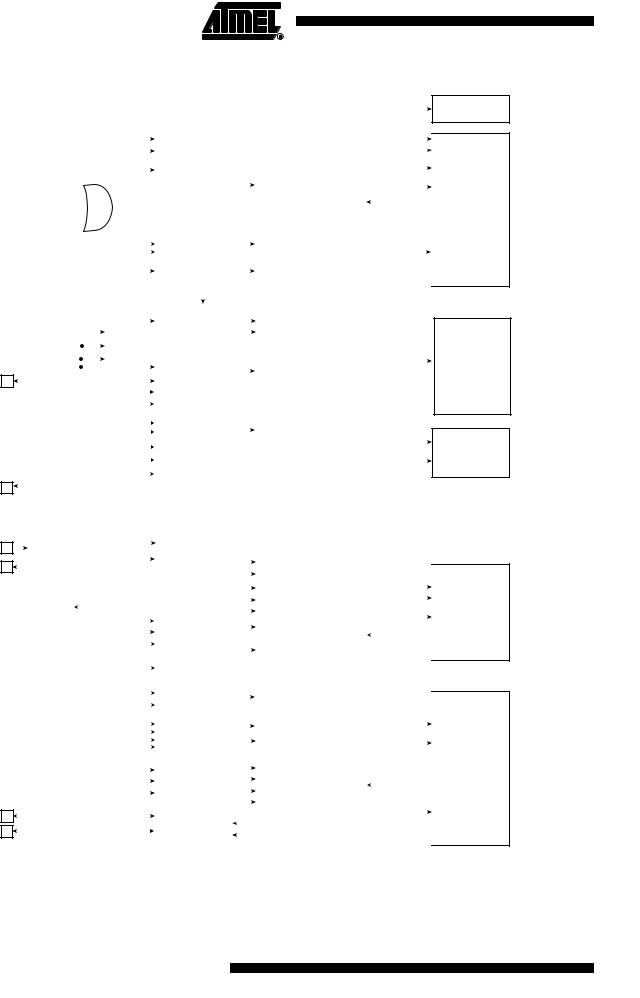
Figure 9-1. |
System Controller Block Diagram |
|
|
|
|
|
|
|
|
||||||||||||||||||||||||||||||||
|
|
|
|
|
|
|
|
|
|
|
|
|
|
|
|
|
|
|
|
|
|
|
|
|
|
|
|
|
|
|
|
|
|
|
|
|
|
jtag_nreset |
|
||
|
|
|
|
|
|
|
|
|
|
|
|
|
|
|
|
|
|
|
|
|
|
|
|
|
|
|
|
|
|
System Controller |
|
|
|
|
|||||||
|
|
|
|
|
|
|
|
|
|
irq0-irq1-irq2-irq3 |
|
|
|
|
|
|
|
|
|
|
|
|
|
|
|
|
|
|
nirq |
|
|
||||||||||
|
|
|
|
|
|
|
|
|
|
|
|
|
|
|
|
|
|
|
|
|
|
|
|
|
|
|
|
|
|
|
|
|
|||||||||
|
|
|
|
|
|
|
|
|
|
|
|
|
|
|
|
|
|
|
|
|
|
|
|
|
|
|
|
|
|
|
|
|
|||||||||
|
|
|
|
|
|
|
|
|
|
|
|
|
|
|
|
|
|
|
|
|
|
|
|
|
|
|
|
|
|
|
|
|
|||||||||
|
|
|
|
|
|
|
|
|
|
|
|
|
fiq |
|
|
|
|
|
|
|
|
|
|
|
|
|
|
|
|
|
|
|
|
|
|
nfiq |
|
||||
|
|
|
|
|
|
|
|
|
|
|
|
|
|
|
|
|
|
|
|
|
|
|
|
Advanced |
|
|
|
|
|
proc_nreset |
|
|
|
||||||||
|
|
|
|
|
|
|
|
|
|
periph_irq[2..27] |
|
|
|
|
|
|
|
|
|
|
|
|
|
|
|
|
|
|
|
|
|
|
|
|
|||||||
|
|
|
|
|
|
|
|
|
|
|
|
|
|
|
|
|
|
|
|
|
|
|
|
|
|
Interrupt |
|
|
|
int |
|
PCK |
|
|
|
||||||
|
|
|
|
|
|
|
|
|
|
|
|
|
|
|
|
|
|
|
|
|
|
|
|
|
|
|
|
||||||||||||||
|
|
|
|
|
|
|
|
|
|
|
|
|
|
|
|
|
|
|
|
|
|
|
|
|
|
|
|
|
|
|
|
|
|
|
|
|
|
||||
|
|
|
|
|
|
|
|
|
|
pit_irq |
|
|
|
|
|
|
|
|
|
|
|
|
|
|
|
|
|
|
|
|
Controller |
|
|
|
|
|
|
|
|||
|
|
|
|
|
|
|
|
|
|
|
|
|
|
|
|
|
|
|
|
|
|
|
|
|
|
|
|
|
|
|
|
|
|
|
|||||||
|
|
|
|
|
|
|
|
|
|
|
|
|
|
|
|
|
|
|
|
|
|
|
|
|
|
|
|
|
|
|
|
|
|
|
|
|
|
||||
|
|
|
|
|
|
|
|
|
|
rtt_irq |
|
|
|
|
|
|
|
|
|
|
|
|
|
|
|
|
|
|
|
|
|
|
|
|
|
|
|
debug |
|
||
|
|
|
|
|
|
|
|
|
|
wdt_irq |
|
|
|
|
|
|
|
|
|
|
|
|
|
|
|
|
|
|
|
|
|
|
|
|
|
|
|
|
|||
|
|
|
|
|
|
|
|
|
|
|
|
|
|
|
|
|
|
|
|
|
|
|
|
|
|
|
|
|
|
|
|
|
|
|
|
|
|
|
|
|
|
|
|
|
|
|
|
|
|
|
|
dbgu_irq |
|
|
|
|
|
|
|
|
|
|
|
|
|
|
|
|
|
|
|
|
|
|
|
|
|
|
|
|
|
|
|
|
|
|
|
|
|
|
|
|
|
|
|
|
|
|
|
|
|
|
|
|
|
|
|
|
|
|
|
|
|
|
|
|
|
|
|
|
|
|
|
|
|
|
|
|
|
|
|
|
|
|
|
pmc_irq |
|
|
|
|
|
|
|
|
|
|
|
|
|
|
|
|
|
|
|
|
|
|
|
|
|
|
|
|
|
|
|
|
|
|
|
|
|
|
|
|
|
rstc_irq |
|
|
|
|
|
|
|
|
|
|
|
|
|
|
|
|
|
|
|
|
|
|
|
|
|
dbgu_irq |
|
|
|
|
|
|
|
|
|
|
|
|
|
|
|
|
|
MCK |
|
|
|
|
|
|
|
|
ice_nreset |
|
|||||||||||||||||||
|
|
|
|
|
|
|
|
|
|
|
|
|
|
|
|
|
|
|
|
|
|||||||||||||||||||||
|
|
|
|
|
|
|
|
|
|
|
|
|
|
Debug |
|
|
|
|
|
||||||||||||||||||||||
|
|
|
|
|
|
|
|
|
|
|
|
|
|
|
|
|
|
|
|||||||||||||||||||||||
|
|
|
|
|
|
|
|
|
|
periph_nreset |
|
|
|
|
|
|
|
|
|
|
|
|
|||||||||||||||||||
|
|
|
|
|
|
|
|
|
|
|
|
|
|
|
|
|
|
|
|
|
|
||||||||||||||||||||
|
|
|
|
|
|
|
|
|
|
dbgu_rxd |
|
|
|
|
Unit |
|
|
|
dbgu_txd |
|
|
|
|
|
|||||||||||||||||
|
|
|
|
|
|
|
|
|
|
|
|
|
|
|
|
|
|
|
|
|
|
|
|||||||||||||||||||
|
|
|
|
|
|
|
|
|
|
|
|
|
|
|
|
|
|
|
|
|
|
|
|||||||||||||||||||
|
|
|
|
|
|
|
|
|
|
|
|
|
|
|
|
|
|
|
|
|
|
|
|
|
|
|
|
|
|
|
|
|
|
|
|
|
|
|
|
|
|
|
|
|
|
|
|
|
|
|
|
|
|
|
|
|
|
|
|
|
|
|
|
|
|
|
|
|
|
|
|
|
|
wdt_fault |
|
|
|
|
|
|
|
|
|
|
|
|
|
|
|
|
|
|
|
|
|
|
|
|
|
|
|
|
|
|
|
|
|
|
|
|
|
|
|
|
|
|
|
|
|
|
|
|
|||
|
|
|
|
|
|
|
|
|
|
|
|
|
|
|
|
|
|
|
|
|
|
|
|
|
|
|
|
|
|
|
|
WDRPROC |
|
|
|
|
|
|
|
|
|
|
|
|
|
|
|
|
|
|
|
|
|
|
|
|
|
|
|
|
|
|
|
|
|
|
|
|
|
|
|
|
|
|
|
|
|
|
|
|
|
|
|
|
|
|
|
|
|
|
|
|
|
VDD3V3 |
|
|
|
|
|
|
|
|
|
|
|
|
|
|
|
|
|
|
|
|
|
|
|
|
|
periph_nreset |
|
|
|
|
|
|
|
|
|
|
|
|
|
|
|
POR |
|
|
|
|
|
|
|
|
|
|
|
|
|
|
|
|
|
|
ice_nreset |
|
|
|
|
|
|
proc_nreset |
|
|
|
|
|
|
|
|
|
|
|
|
|
|
|
|
|
|
|
|
|
|
|
|
|
|
|
|
|
|
|
|
|
|
jtag_nreset |
|
Reset |
|
|
|
|
|
|
|
|
|
|
|
|
|
|
|
|
|
|
|
|
VDD1V8 |
|
|
|
|
|
|
|
|
|
|
|
|
|
|
|
|
|
|
flash_poe |
|
|
|
|
|
|
proc_nreset |
|||||
|
NRST |
|
|
POR |
|
|
|
|
|
|
|
|
|
|
|
|
|
|
|
|
|
|
|
|
Controller |
|
|
|
rstc_irq |
|
|
|
|
|
|||||||
|
|
|
|
|
|
|
|
|
|
|
|
|
|
|
|
|
|
|
|
|
|
|
|
|
|
|
|
|
|
|
|||||||||||
|
|
|
|
|
|
|
|
|
|
|
|
|
|
|
|
|
|
|
|
|
|
|
|
|
|
|
|
|
|
|
|
|
|
||||||||
|
|
|
|
|
|
|
|
|
|
|
|
|
|
|
|
|
|
|
|
|
|
|
|
|
|
|
|
|
|
|
|
|
|
|
|||||||
|
|
|
|
|
|
|
|
|
|
|
|
|
|
|
|
|
|
|
|
|
|
|
|
|
|
|
|
|
|
|
|
|
|
|
|||||||
|
|
|
|
|
|
|
|
|
|
|
|
|
SLCK |
|
|
|
|
|
|
|
|
|
|
|
|
|
|||||||||||||||
|
|
|
|
|
|
|
|
|
|
VDDBU |
|
|
|
|
|
|
|
|
|
VDD1V8 Powered |
|
|
|
|
|
||||||||||||||||
|
|
|
|
|
|
|
|
|
|
|
|
|
|
|
|
|
|
|
|
|
|
|
|
|
|
|
|
|
|
|
|
|
|
|
|
|
|
|
|
||
|
|
|
|
|
|
|
|
|
|
POR |
|
|
|
|
|
|
|
|
|
|
|
|
|
|
|
|
|
|
|
|
|
|
|
|
|
|
|
|
|
|
|
|
|
|
|
|
|
|
|
|
|
|
|
|
|
|
|
|
|
|
|
|
|
|
|
|
|
|
|
|
|
|
|
|
|
|
|
|
|
|
|
|
|
|
|
|
|
|
|
|
|
|
|
|
|
SLCK |
|
|
|
Real-Time |
|
|
|
rtt_irq |
|
|
|
|
|
||||||||||||||||
|
|
|
|
|
|
|
|
|
|
|
|
|
|
|
|
|
|
|
|
|
|
|
|||||||||||||||||||
|
FWKUP |
|
|
|
|
|
|
|
|
periph_nreset |
|
|
|
Timer |
|
|
|
|
MCK |
|
|||||||||||||||||||||
|
|
|
|
|
|
|
|
|
|
|
|
|
|
|
|
|
|
|
|
|
|
|
|
|
|
|
|
|
|
|
|
|
|
|
|
|
|||||
|
|
|
|
|
|
|
|
|
|
|
|
|
|
|
|
|
|
|
|
|
|
|
|
|
|
|
|
|
|
|
|
|
|
|
|
|
proc_nreset |
||||
|
WKUP0 |
|
|
|
|
|
|
|
|
|
|
|
|
|
|
|
|
|
|
|
|
|
|
|
|
|
|
|
|
|
Shutdown |
|
|
|
|
|
|||||
|
|
|
|
|
|
|
|
|
|
|
|
|
|
|
|
|
|
|
|
|
|
|
|
|
|
|
|
|
|
|
|
|
|
|
|||||||
|
|
|
|
|
|
|
|
|
|
|
|
|
|
|
|
|
|
|
|
|
|
|
|
|
|
|
|
|
|
|
|
|
|
||||||||
|
|
|
|
|
|
|
|
|
|
|
|
|
|
|
|
|
|
|
|
|
|
|
|
|
|
|
|
|
|
|
|
|
|
|
|
|
|
|
|
||
|
WKUP1 |
|
|
|
|
|
|
|
|
|
|
|
|
|
|
|
|
|
|
|
|
|
|
|
|
|
|
|
|
|
Controller |
|
|
|
|
|
|
|
|
|
|
|
|
|
|
|
|
|
|
|
|
|
|
|
|
|
|
|
|
|
|
|
|
|
|
|
|
|
|
|
|
|
|
|
|
|
|
|
|
|
|||
|
SHDW |
|
|
|
|
|
|
|
|
|
|
|
|
|
|
|
|
|
|
|
|
|
|
|
|
|
|
|
|
|
|
|
|
|
|
|
|||||
|
|
|
|
VDDBU Powered |
|
|
|
|
|
|
|
|
|
|
|
|
|||||||||||||||||||||||||
|
|
|
|
|
|
|
|
|
|
|
|
|
|
|
|
|
|
|
|
|
|
||||||||||||||||||||
|
|
|
|
|
|
|
|
|
|
|
|
|
|
|
|
|
|
|
|
|
|
|
|
|
|
|
|
|
|
|
|
|
|
|
|
|
|
|
|
|
|
|
|
|
|
|
|
|
|
|
|
|
|
|
SLCK |
|
4 General-Purpose |
|
|
|
|
|
|
|
|
|
|||||||||||||||||
|
|
|
|
|
|
|
|
|
|
RCOSC |
|
|
|
Backup Regs |
|
|
|
|
|
|
|
|
|
||||||||||||||||||
|
XIN |
|
|
|
|
|
|
|
|
|
|
|
|
|
|
|
|
|
|
|
|
|
|
|
|
|
|
|
|
|
|
|
|
|
|
|
|||||
|
|
|
|
|
|
|
|
|
|
|
|
|
|
|
|
|
|
|
|
|
|
|
|
|
|
|
|
|
|
|
|
|
|
|
|
|
|
|
|||
|
|
|
|
|
|
|
|
|
|
|
|
|
|
|
|
|
|
|
|
|
|
|
|
|
|
|
|
|
|
|
|
|
|
|
|
|
|
|
|||
|
|
|
|
|
|
|
|
|
|
|
|
|
|
|
|
|
|
|
|
|
|
|
|
|
|
|
|
|
|
|
|
|
|
|
|
|
|||||
|
|
|
|
|
|
|
|
|
|
MAIN |
|
MAINCK |
|
|
|
|
|
|
periph_clk[2..27] |
|
|
|
|
|
|||||||||||||||||
|
XOUT |
|
|
|
|
OSC |
|
|
|
|
|
|
|
|
|
|
|
|
|
|
|
|
|
|
|
|
|
|
|
|
|
|
|
|
|
|
|||||
|
|
|
|
|
|
|
|
|
|
|
|
|
|
|
|
|
|
|
|
|
|
|
|
|
|
|
|
pck[0-3] |
|
UDPCK |
|
||||||||||
|
|
|
|
|
|
|
|
|
|
|
|
|
|
|
|
|
|
|
|
|
|
|
|
|
|
|
|
|
|
|
|
|
|
|
|
|
|||||
|
|
|
|
|
|
|
|
|
|
|
|
|
|
|
|
|
|
|
|
|
|
|
|
|
|
|
|
|
|
|
|
|
|
|
|
|
|||||
|
|
|
|
|
|
|
|
|
|
|
|
|
|
|
|
|
|
|
|
|
|
|
|
|
|
|
|
|
|
|
|
|
|
|
|
PCK |
|
||||
|
|
|
|
|
|
|
|
|
|
|
|
|
|
|
|
|
|
|
|
|
|
|
|
|
|
|
|
|
|
|
Power |
|
|
|
|
periph_clk[27] |
|||||
|
|
|
|
|
|
|
|
|
|
|
|
|
|
|
|
|
|
|
|
|
|
|
|
|
|
|
|
|
|
|
|
|
|
UDPCK |
|
||||||
|
|
|
|
|
|
|
|
|
|
|
|
|
|
|
|
|
|
|
|
|
|
|
|
|
|
|
|
|
|
|
Management |
|
|
|
|
|
|
|
|
||
|
PLLRC |
|
|
|
|
|
|
|
PLL |
|
|
|
|
|
|
|
|
|
|
|
|
|
|
|
|
|
|
PLLCK |
|
Controller |
|
|
|
MCK |
|
periph_nreset |
|
|
|||
|
|
|
|
|
|
|
|
|
|
|
|
|
|
|
|
|
|
|
|
|
|
|
|
|
|
pmc_irq |
|
|
|||||||||||||
|
|
|
|
|
|
|
|
|
|
|
|
|
|
|
|
|
|
|
|
|
|
|
|
periph_irq[27] |
|||||||||||||||||
|
|
|
|
|
|
|
|
|
|
|
|
|
int |
|
|
|
|
|
|
|
|
|
|
|
|
|
|
|
|
|
|
|
|
||||||||
|
|
|
|
|
|
|
|
|
|
|
|
|
|
|
|
|
|
|
|
|
|
|
|
|
|
|
|
|
|
|
|
|
|||||||||
|
|
|
|
|
|
|
|
|
|
|
|
|
|
|
|
|
|
|
|
|
|
|
|
|
|
|
|
|
|
|
|
|
|||||||||
|
|
|
|
|
|
|
|
|
|
|
|
|
|
|
|
|
|
|
|
|
|
|
|
|
|
|
|
|
|
|
|||||||||||
|
|
|
|
|
|
|
|
|
|
|
|
|
|
|
|
|
|
|
|
|
|
|
|
|
|
|
|
|
|
||||||||||||
|
|
|
|
|
|
|
|
|
|
periph_nreset |
|
|
|
|
|
|
|
|
|
|
|
|
|
|
|
|
|
idle |
|
|
|
|
|
||||||||
|
|
|
|
|
|
|
|
|
|
|
|
|
|
|
|
|
|
|
|
|
|
|
|
|
|
|
|
|
|
||||||||||||
|
|
|
|
|
|
|
|
|
|
|
|
MCK |
|
|
|
|
|
|
|
|
|
|
|
|
|
||||||||||||||||
|
|
|
|
|
|
|
|
|
|
|
|
|
|
|
|
|
|
|
|
|
|
|
|
|
|||||||||||||||||
|
|
|
|
|
|
|
|
|
|
|
|
|
|
|
|
|
|
|
|
|
|
|
|
|
|
||||||||||||||||
|
|
|
|
|
|
|
|
|
|
|
|
|
|
|
|
|
|
|
|
|
|
|
|
|
|
||||||||||||||||
|
|
|
|
|
|
|
|
|
|
|
|
|
|
|
|
|
|
|
|
|
|
|
|
|
|
||||||||||||||||
|
|
|
|
|
|
|
|
|
|
|
|
|
|
|
|
|
|
|
|
|
|
|
|
|
|
|
|
|
|
|
|
|
|
|
|
|
|
|
|
|
|
|
|
|
|
|
|
|
|
|
|
|
|
|
|
|
|
|
|
|
|
|
|
|
|
|
|
|
|
|
|
|
|
|
|
|
|
|
|
|
|
|
|
|
|
|
|
|
|
|
|
|
|
|
debug |
|
|
|
|
|
Periodic |
|
|
|
|
|
|
|
|
|
|||||||||||||||
|
|
|
|
|
|
|
|
|
|
periph_nreset |
|
|
|
|
|
|
|
|
|
Interval |
|
|
|
pit_irq |
|
|
|
|
|
||||||||||||
|
|
|
|
|
|
|
|
|
|
|
|
|
|
|
Timer |
|
|
|
|
periph_clk[4..26] |
|
||||||||||||||||||||
|
|
|
|
|
|
|
|
|
|
|
|
|
|
|
|
|
|
|
|
||||||||||||||||||||||
|
|
|
|
|
|
|
|
|
|
|
|
SLCK |
|
|
|
|
|
|
|
|
|
|
|
|
wdt_irq |
|
|||||||||||||||
|
|
|
|
|
|
|
|
|
|
|
|
|
|
|
|
|
|
|
Watchdog |
|
|
|
|||||||||||||||||||
|
|
|
|
|
|
|
|
|
|
|
|
|
|
|
|
|
|
|
|
|
|
|
|
|
|
||||||||||||||||
|
|
|
|
|
|
|
|
|
|
|
|
|
|
|
|
|
|
|
|
||||||||||||||||||||||
|
|
|
|
|
|
|
|
|
|
|
debug |
|
|
|
|
|
wdt_fault |
|
periph_nreset |
|
|||||||||||||||||||||
|
|
|
|
|
|
|
|
|
|
|
|
|
|
|
|
|
|
||||||||||||||||||||||||
|
|
|
|
|
|
|
|
|
|
|
|
|
idle |
|
|
Timer |
|
|
|
|
|
||||||||||||||||||||
|
|
|
|
|
|
|
|
|
|
|
|
|
|
|
|
|
|
|
|
||||||||||||||||||||||
|
|
|
|
|
|
|
|
|
|
proc_nreset |
|
|
|
|
|
|
|
|
|
WDRPROC |
|
|
|
|
|
||||||||||||||||
|
|
|
|
|
|
|
|
|
|
|
|
|
|
|
|
|
|
|
|
|
|
|
|
||||||||||||||||||
|
|
|
|
|
|
|
|
|
|
|
|
|
|
|
|
|
|
|
|
|
|
|
|
||||||||||||||||||
|
|
|
|
|
|
|
|
|
|
periph_nreset |
|
|
|
|
|
|
|
|
|
|
|
|
|
|
|
|
|
|
|
periph_irq{2..3] |
|
|
|
|
|
||||||
|
|
|
|
|
|
|
|
|
|
periph_clk[2..3] |
|
|
|
|
|
|
|
|
|
|
|
|
|
|
|
|
|
irq0-irq1-irq2-irq3 |
|
periph_irq[4..26] |
|
||||||||||
|
|
|
|
|
|
|
|
|
|
|
|
|
|
|
|
|
|
|
|
|
|
|
|
|
|
|
|
|
|
|
|||||||||||
|
|
|
|
|
|
|
|
|
|
|
|
|
|
|
|
|
|
|
|
|
|
|
|
|
|
|
|
|
|||||||||||||
|
|
|
|
|
|
|
|
|
|
dbgu_rxd |
|
|
|
|
|
|
|
|
|
|
|
|
|
|
PIOs |
|
|
|
fiq |
|
|
|
|
|
|||||||
|
|
|
|
|
|
|
|
|
|
|
|
|
|
|
|
|
|
|
|
|
|
|
|
|
|
|
|
|
|
|
|
||||||||||
|
|
|
|
|
|
|
|
|
|
|
|
|
|
|
|
|
|
|
|
|
|
|
dbgu_txd |
|
|
|
|
|
|||||||||||||
|
|
|
|
|
|
|
|
|
|
|
|
|
|
|
|
|
|
|
|
|
|
|
|
|
|
|
|
|
|
|
|
|
|
|
|
|
|
|
|||
|
PA0-PA31 |
|
|
|
|
|
|
|
|
|
|
|
|
|
|
|
|
|
|
|
|
|
|
|
|
Controller |
|
|
|
|
in |
|
|
||||||||
|
|
|
|
|
|
|
|
|
|
|
|
|
|
|
|
|
|
|
|
|
|
|
|
|
|
|
|
|
|
|
|||||||||||
|
|
|
|
|
|
|
|
|
|
|
|
|
|
|
|
|
|
|
|
|
|
|
|
|
|
|
|
|
|
|
|
out |
|
||||||||
|
|
|
|
|
|
|
|
|
|
|
|
|
|
|
|
|
|
|
|
|
|
|
|
|
|
|
|
|
|
|
|
|
|||||||||
|
|
|
|
|
|
|
|
|
|
|
|
|
|
|
|
|
|
|
|
|
|
|
|
|
|
|
|
|
|
|
|
|
|
|
|
|
|
|
|||
|
PB0-PB29 |
|
|
|
|
|
|
|
|
|
|
|
|
|
|
|
|
|
|
|
|
|
|
|
|
|
|
|
|
|
enable |
|
|||||||||
|
|
|
|
|
|
|
|
|
|
|
|
|
|
|
|
|
|
|
|
|
|
|
|
|
|
|
|
|
|
|
|||||||||||
|
|
|
|
|
|
|
|
|
|
|
|
|
|
|
|
|
|
|
|
|
|
|
|
|
|
|
|
|
|
|
|
|
|
|
|
|
|
|
|
|
|
Boundary Scan
TAP Controller
ARM7TDMI
Embedded Flash
Memory
Controller
USB Device
Port
Embedded
Peripherals
9.1System Controller Mapping
20 AT91SAM7A3 Preliminary
6042E–ATARM–14-Dec-06
AT91SAM7A3 Preliminary
9.2Reset Controller
The Reset Controller is based on three power-on reset cells. It gives the status of the last reset, indicating whether it is a general reset, a wake-up reset, a software reset, a user reset or a watchdog reset. In addition, it controls the internal resets and the NRST pin output. It shapes a signal on the NRST line, guaranteeing that the length of the pulse meets any requirement.
9.3Clock Generator
The Clock Generator embeds one low-power RC Oscillator, one Main Oscillator and one PLL with the following characteristics:
–RC Oscillator ranges between 22 KHz and 42 KHz
–Main Oscillator frequency ranges between 3 and 20 MHz
–Main Oscillator can be bypassed
–PLL output ranges between 80 and 220 MHz
It provides SLCK, MAINCK and PLLCK.
Figure 9-2. Clock Generator Block Diagram
|
|
|
|
|
Clock Generator |
|
|
||||||
|
|
|
|
|
|
|
|
|
|
|
|
|
|
|
|
|
|
|
|
Embedded |
|
|
|
|
Slow Clock |
||
|
|
|
|
|
|
RC |
|
|
|
|
|||
|
|
|
|
|
|
|
|
|
|
SLCK |
|||
|
|
|
|
|
|
Oscillator |
|
|
|
|
|||
|
|
|
|
|
|
|
|
|
|
|
|||
XIN |
|
|
|
|
|
|
|
|
|
|
|
|
|
|
|
|
|
|
|
|
|
|
|
|
|
|
|
|
|
|
|
|
Main |
|
|
|
|
Main Clock |
|||
|
|
|
|
|
|
|
|
|
|||||
|
|
|
|
|
|
|
|
|
|
||||
XOUT |
|
|
|
|
|
Oscillator |
|
|
|
|
MAINCK |
||
|
|
|
|
|
|
|
|
||||||
|
|
|
|
|
|
|
|
|
|
|
|
|
|
|
|
|
|
|
|
|
|
|
|
|
|
|
|
|
|
|
|
|
|
|
|
|
|
|
|
|
|
|
|
|
|
|
|
|
|
|
|
|
|
|
|
|
|
|
|
|
|
|
|
|
|
|
|
|
|
|
|
|
|
|
|
PLL and |
|
|
|
|
PLL Clock |
||
|
|
|
|
|
|
|
|
|
|
||||
PLLRC |
|
|
|
|
|
Divider |
|
|
|
|
PLLCK |
||
|
|
|
|
|
|
|
|
|
|||||
|
|
|
|
|
|
|
|
|
|
|
|
|
|
|
|
|
|
|
|
|
|
|
|
|
|
|
|
|
|
|
|
|
|
Status |
|
|
Control |
||||
|
|
|
|
|
|
|
|||||||
|
|
|
|
|
|
|
|
|
|
|
|
|
|
|
|
|
|
|
|
Power |
|
|
|
|
|
||
|
|
|
|
|
|
Management |
|
|
|
||||
|
|
|
|
|
|
Controller |
|
|
|
|
|
||
|
|
|
|
|
|
|
|
|
|
|
|
|
|
9.4Power Management Controller
The Power Management Controller uses the Clock Generator outputs to provide:
–the Processor Clock PCK
–the Master Clock MCK
–the USB Clock UDPCK
–all the peripheral clocks, independently controllable
–four programmable clock outputs
The Master Clock (MCK) is programmable from a few hundred Hz to the maximum operating frequency of the device.
The Processor Clock (PCK) switches off when entering processor idle mode, thereby reducing power consumption while waiting an interrupt.
21
6042E–ATARM–14-Dec-06

Figure 9-3. Power Management Controller Block Diagram
|
|
Master Clock Controller |
|||
SLCK |
|
|
|
Prescaler |
|
|
|
|
|||
MAINCK |
|
|
|
||
|
|
|
|||
PLLCK |
|
|
|
|
/1,/2,/4,...,/64 |
|
|
|
|
||
Processor |
PCK |
|
Clock |
||
|
||
Controller |
int |
|
|
||
Idle Mode |
|
|
|
MCK |
|
Peripherals |
periph_clk[2..26] |
|
Clock Controller |
||
|
||
ON/OFF |
|
|
|
|
Programmable Clock Controller |
|
||||||
SLCK |
|
|
|
|
|
Prescaler |
|
|
||
|
|
|
|
|
|
|||||
MAINCK |
|
|
|
|
|
pck[0..3] |
||||
|
||||||||||
PLLCK |
|
/1,/2,/4,...,/64 |
|
|
||||||
|
|
|
|
|||||||
|
|
|
USB Clock Controller |
|
||||||
|
|
|
|
|
|
ON/OFF |
|
|||
|
|
|
|
|
|
|
|
|
||
PLLCK |
|
|
|
|
Divider |
|
|
|
UDPCK |
|
|
|
|
/1,/2,/4 |
|
|
|
||||
|
|
|
|
|
|
|
||||
|
|
|
|
|
|
|
|
|
|
|
9.5Advanced Interrupt Controller
•Controls the interrupt lines (nIRQ and nFIQ) of the ARM Processor
•Individually maskable and vectored interrupt sources
–Source 0 is reserved for the Fast Interrupt Input (FIQ)
–Source 1 is reserved for system peripherals (ST, PMC, DBGU, etc.)
–Other sources control the peripheral interrupts or external interrupts
–Programmable edge-triggered or level-sensitive internal sources
–Programmable positive/negative edge-triggered or high/low level-sensitive external sources (FIQ, IRQ)
•8-level Priority Controller
–Drives the normal interrupt nIRQ of the processor
–Handles priority of the interrupt sources
–Higher priority interrupts can be served during service of a lower priority interrupt
•Vectoring
–Optimizes interrupt service routine branch and execution
–One 32-bit vector register per interrupt source
–Interrupt vector register reads the corresponding current interrupt vector
•Protect Mode
–Easy debugging by preventing automatic operations
•Fast Forcing
–Permits redirecting any interrupt source on the fast interrupt
•General Interrupt Mask
–Provides processor synchronization on events without triggering an interrupt
22 AT91SAM7A3 Preliminary 
6042E–ATARM–14-Dec-06

AT91SAM7A3 Preliminary
9.6Debug Unit
•Comprises
–One two-pin UART
–One interface for the Debug Communication Channel (DCC) support
–One set of chip ID registers
–One interface allowing ICE access prevention
•Two-pin UART
–USART-compatible user interface
–Programmable baud rate generator
–Parity, framing and overrun error
–Automatic Echo, Local Loopback and Remote Loopback Channel Modes
•Debug Communication Channel Support
–Offers visibility of COMMRX and COMMTX signals from the ARM Processor
•Chip ID Registers
–Identification of the device revision, sizes of the embedded memories, set of peripherals
–Chip ID is 0x260A0941 (Version 1)
9.7Period Interval Timer
•20-bit programmable counter plus 12-bit interval counter
9.8Watchdog Timer
•12-bit key-protected Programmable Counter running on prescaled SLCK
•Provides reset or interrupt signals to the system
•Counter may be stopped while the processor is in debug state or in idle mode
9.9Real-time Timer
•32-bit free-running counter with alarm
•Programmable 16-bit prescaler for SCLK accuracy compensation
9.10Shutdown Controller
•Software programmable assertion of the SHDW open-drain pin
•De-assertion programmable with the pins WKUP0, WKUP1 and FWKUP
9.11PIO Controllers A and B
•The PIO Controllers A and B respectively control 32 and 30 programmable I/O Lines
•Fully programmable through Set/Clear Registers
•Multiplexing of two peripheral functions per I/O Line
•For each I/O Line (whether assigned to a peripheral or used as general purpose I/O)
–Input change interrupt
–Half a clock period Glitch filter
–Multi-drive option enables driving in open drain
23
6042E–ATARM–14-Dec-06

–Programmable pull up on each I/O line
–Pin data status register, supplies visibility of the level on the pin at any time
•Synchronous output, provides Set and Clear of several I/O lines in a single write
24 AT91SAM7A3 Preliminary 
6042E–ATARM–14-Dec-06

AT91SAM7A3 Preliminary
10. Peripherals
10.1Peripheral Mapping
Each User Peripheral is allocated 16K bytes of address space.
Figure 10-1. User Peripherals Mapping
Address |
Peripheral |
Peripheral Name |
Size |
|
0xF000 0000 |
|
|
|
|
|
|
Reserved |
|
|
0xFFF7 FFFF |
|
|
|
|
0xFFF8 0000 |
CAN0 |
CAN Controller 0 |
16K Bytes |
|
|
|
|||
0xFFF8 3FFF |
|
|
|
|
0xFFF8 4000 |
CAN1 |
CAN Controller 1 |
16K Bytes |
|
|
|
|||
0xFFF8 7FFF |
|
|
|
|
0xFFF8 8000 |
|
|
|
|
|
|
Reserved |
|
|
0xFFF9 FFFF |
|
|
|
|
0xFFFA 0000 |
TC0, TC1, TC2 |
Timer/Counter 0, 1 and 2 |
16K Bytes |
|
|
|
|||
0xFFFA 3FFF |
|
|
|
|
0xFFFA 4000 |
TC3, TC4, TC5 |
Timer/Counter 3, 4 and 5 |
16K Bytes |
|
|
|
|||
0xFFFA 7FFF |
|
|
|
|
0xFFFA 8000 |
TC6, TC7, TC8 |
Timer/Counter 6, 7 and 8 |
16K Bytes |
|
|
|
|||
0xFFFA BFFF |
|
|
|
|
0xFFFA C000 |
MCI |
Multimedia Card Interface |
16K Bytes |
|
|
|
|||
0xFFFA FFFF |
|
|
|
|
0xFFFB 0000 |
UDP |
USB Device Port |
16K Bytes |
|
|
|
|||
0xFFFB 3FFF |
|
|
|
|
0xFFFB 4000 |
|
|
|
|
|
|
Reserved |
|
|
0xFFFB 7FFF |
|
|
|
|
0xFFFB 8000 |
TWI |
Two-Wire Interface |
16K Bytes |
|
|
|
|||
0xFFFB BFFF |
|
|
|
|
0xFFFB C000 |
|
|
|
|
|
|
Reserved |
|
|
0xFFFB FFFF |
|
|
|
|
0xFFFC 0000 |
USART0 |
Universal Synchronous Asynchronous |
16K Bytes |
|
|
|
|||
0xFFFC 3FFF |
|
Receiver Transmitter 0 |
|
|
|
|
|
||
0xFFFC 4000 |
USART1 |
Universal Synchronous Asynchronous |
16K Bytes |
|
|
|
|||
0xFFFC 7FFF |
|
Receiver Transmitter 1 |
|
|
|
|
|
||
0xFFFC 8000 |
USART2 |
Universal Synchronous Asynchronous |
16K Bytes |
|
|
|
|||
0xFFFC BFFF |
|
|
Receiver Transmitter 1 |
|
|
|
|
|
|
0xFFFC C000 |
|
PWMC |
PWM Controller |
16K Bytes |
|
|
|||
|
|
|
||
0xFFFC FFFF |
|
|
|
|
0xFFFD 0000 |
SSC0 |
Serial Synchronous Controller 0 |
16K Bytes |
|
|
|
|||
0xFFFD 3FFF |
|
|
|
|
0xFFFD 4000 |
SSC1 |
Serial Synchronous Controller 1 |
16K Bytes |
|
|
|
|||
0xFFFD 7FFF |
|
|
|
|
0xFFFD 8000 |
ADC0 |
Analog-to-Digital Converter 0 |
16K Bytes |
|
|
|
|||
0xFFFD BFFF |
|
|
|
|
0xFFFD C000 |
ADC1 |
Analog-to-Digital Converter 1 |
16K Bytes |
|
|
|
|||
0xFFFD FFFF |
|
|
|
|
0xFFFE 0000 |
SPI0 |
Serial Peripheral Interface 0 |
16K Bytes |
|
|
|
|||
0xFFFE 3FFF |
|
|
||
|
|
|
||
0xFFFE 4000 |
SPI1 |
Serial Peripheral Interface 1 |
16K Bytes |
|
|
|
|||
0xFFFE 7FFF |
|
|
||
|
|
|
||
0xFFFE 8000 |
|
|
|
|
|
|
Reserved |
|
|
0xFFFE FFFF |
|
|
|
|
25
6042E–ATARM–14-Dec-06

10.2Peripheral Multiplexing on PIO Lines
The AT91SAM7A3 features two PIO controllers, PIOA and PIOB, which multiplex the I/O lines of the peripheral set.
PIO Controllers A and B control respectively 32 and 30 lines. Each line can be assigned to one of two peripheral functions, A or B. Some of them can also be multiplexed with Analog Input of both ADC Controllers.
Table 10-1 on page 27 and Table 10-2 on page 28 define how the I/O lines of the peripherals A, B or Analog Input are multiplexed on the PIO Controllers A and B. The two columns “Function” and “Comments” have been inserted for the user’s own comments; they may be used to track how pins are defined in an application.
Note that some peripheral functions that are output only may be duplicated within both tables.
At reset, all I/O lines are automatically configured as input with the programmable pull-up enabled, so that the device is maintained in a static state as soon as a reset occurs.
26 AT91SAM7A3 Preliminary 
6042E–ATARM–14-Dec-06

AT91SAM7A3 Preliminary
10.3PIO Controller A Multiplexing
Table 10-1. |
Multiplexing on PIO Controller A |
|
|
|
|
||
|
|
PIO Controller A |
|
Application Usage |
|
||
|
|
|
|
|
|
|
|
I/O Line |
Peripheral A |
|
Peripheral B |
Comment |
Function |
|
Comments |
|
|
|
|
|
|
|
|
PA0 |
TWD |
|
ADC0_ADTRG |
|
|
|
|
|
|
|
|
|
|
|
|
PA1 |
TWCK |
|
ADC1_ADTRG |
|
|
|
|
|
|
|
|
|
|
|
|
PA2 |
RXD0 |
|
|
|
|
|
|
|
|
|
|
|
|
|
|
PA3 |
TXD0 |
|
|
|
|
|
|
|
|
|
|
|
|
|
|
PA4 |
SCK0 |
|
SPI1_NPSC0 |
|
|
|
|
|
|
|
|
|
|
|
|
PA5 |
RTS0 |
|
SPI1_NPCS1 |
|
|
|
|
|
|
|
|
|
|
|
|
PA6 |
CTS0 |
|
SPI1_NPCS2 |
|
|
|
|
|
|
|
|
|
|
|
|
PA7 |
RXD1 |
|
SPI1_NPCS3 |
|
|
|
|
|
|
|
|
|
|
|
|
PA8 |
TXD1 |
|
SPI1_MISO |
|
|
|
|
|
|
|
|
|
|
|
|
PA9 |
RXD2 |
|
SPI1_MOSI |
|
|
|
|
|
|
|
|
|
|
|
|
PA10 |
TXD2 |
|
SPI1_SPCK |
|
|
|
|
|
|
|
|
|
|
|
|
PA11 |
SPI0_NPCS0 |
|
|
|
|
|
|
|
|
|
|
|
|
|
|
PA12 |
SPI0_NPCS1 |
|
MCDA1 |
|
|
|
|
|
|
|
|
|
|
|
|
PA13 |
SPI0_NPCS2 |
|
MCDA2 |
|
|
|
|
|
|
|
|
|
|
|
|
PA14 |
SPI0_NPCS3 |
|
MCDA3 |
|
|
|
|
|
|
|
|
|
|
|
|
PA15 |
SPI0_MISO |
|
MCDA0 |
|
|
|
|
|
|
|
|
|
|
|
|
PA16 |
SPI0_MOSI |
|
MCCDA |
|
|
|
|
|
|
|
|
|
|
|
|
PA17 |
SPI0_SPCK |
|
MCCK |
|
|
|
|
|
|
|
|
|
|
|
|
PA18 |
PWM0 |
|
PCK0 |
|
|
|
|
|
|
|
|
|
|
|
|
PA19 |
PWM1 |
|
PCK1 |
|
|
|
|
|
|
|
|
|
|
|
|
PA20 |
PWM2 |
|
PCK2 |
|
|
|
|
|
|
|
|
|
|
|
|
PA21 |
PWM3 |
|
PCK3 |
|
|
|
|
|
|
|
|
|
|
|
|
PA22 |
PWM4 |
|
IRQ0 |
|
|
|
|
|
|
|
|
|
|
|
|
PA23 |
PWM5 |
|
IRQ1 |
|
|
|
|
|
|
|
|
|
|
|
|
PA24 |
PWM6 |
|
TCLK4 |
|
|
|
|
|
|
|
|
|
|
|
|
PA25 |
PWM7 |
|
TCLK5 |
|
|
|
|
|
|
|
|
|
|
|
|
PA26 |
CANRX0 |
|
|
|
|
|
|
|
|
|
|
|
|
|
|
PA27 |
CANTX0 |
|
|
|
|
|
|
|
|
|
|
|
|
|
|
PA28 |
CANRX1 |
|
TCLK3 |
|
|
|
|
|
|
|
|
|
|
|
|
PA29 |
CANTX1 |
|
TCLK6 |
|
|
|
|
|
|
|
|
|
|
|
|
PA30 |
DRXD |
|
TCLK7 |
|
|
|
|
|
|
|
|
|
|
|
|
PA31 |
DTXD |
|
TCLK8 |
|
|
|
|
|
|
|
|
|
|
|
|
27
6042E–ATARM–14-Dec-06

10.4PIO Controller B Multiplexing
Table 10-2. |
Multiplexing on PIO Controller B |
|
|
|
||
|
|
PIO Controller B |
|
Application Usage |
||
|
|
|
|
|
|
|
I/O Line |
Peripheral A |
|
Peripheral B |
Comment |
Function |
Comments |
|
|
|
|
|
|
|
PB0 |
IRQ2 |
|
PWM5 |
|
|
|
|
|
|
|
|
|
|
PB1 |
IRQ3 |
|
PWM6 |
|
|
|
|
|
|
|
|
|
|
PB2 |
TF0 |
|
PWM7 |
|
|
|
|
|
|
|
|
|
|
PB3 |
TK0 |
|
PCK0 |
|
|
|
|
|
|
|
|
|
|
PB4 |
TD0 |
|
PCK1 |
|
|
|
|
|
|
|
|
|
|
PB5 |
RD0 |
|
PCK2 |
|
|
|
|
|
|
|
|
|
|
PB6 |
RK0 |
|
PCK3 |
|
|
|
|
|
|
|
|
|
|
PB7 |
RF0 |
|
CANTX1 |
|
|
|
|
|
|
|
|
|
|
PB8 |
FIQ |
|
TF1 |
|
|
|
|
|
|
|
|
|
|
PB9 |
TCLK0 |
|
TK1 |
|
|
|
|
|
|
|
|
|
|
PB10 |
TCLK1 |
|
RK1 |
|
|
|
|
|
|
|
|
|
|
PB11 |
TCLK2 |
|
RF1 |
|
|
|
|
|
|
|
|
|
|
PB12 |
TIOA0 |
|
TD1 |
|
|
|
|
|
|
|
|
|
|
PB13 |
TIOB0 |
|
RD1 |
|
|
|
|
|
|
|
|
|
|
PB14 |
TIOA1 |
|
PWM0 |
ADC0_AD0 |
|
|
|
|
|
|
|
|
|
PB15 |
TIOB1 |
|
PWM1 |
ADC0_AD1 |
|
|
|
|
|
|
|
|
|
PB16 |
TIOA2 |
|
PWM2 |
ADC0_AD2 |
|
|
|
|
|
|
|
|
|
PB17 |
TIOB2 |
|
PWM3 |
ADC0_AD3 |
|
|
|
|
|
|
|
|
|
PB18 |
TIOA3 |
|
PWM4 |
ADC0_AD4 |
|
|
|
|
|
|
|
|
|
PB19 |
TIOB3 |
|
SPI1_NPCS1 |
ADC0_AD5 |
|
|
|
|
|
|
|
|
|
PB20 |
TIOA4 |
|
SPI1_NPCS2 |
ADC0_AD6 |
|
|
|
|
|
|
|
|
|
PB21 |
TIOB4 |
|
SPI1_NPCS3 |
ADC0_AD7 |
|
|
|
|
|
|
|
|
|
PB22 |
TIOA5 |
|
|
ADC1_AD0 |
|
|
|
|
|
|
|
|
|
PB23 |
TIOB5 |
|
|
ADC1_AD1 |
|
|
|
|
|
|
|
|
|
PB24 |
TIOA6 |
|
RTS1 |
ADC1_AD2 |
|
|
|
|
|
|
|
|
|
PB25 |
TIOB6 |
|
CTS1 |
ADC1_AD3 |
|
|
|
|
|
|
|
|
|
PB26 |
TIOA7 |
|
SCK1 |
ADC1_AD4 |
|
|
|
|
|
|
|
|
|
PB27 |
TIOB7 |
|
RTS2 |
ADC1_AD5 |
|
|
|
|
|
|
|
|
|
PB28 |
TIOA8 |
|
CTS2 |
ADC1_AD6 |
|
|
|
|
|
|
|
|
|
PB29 |
TIOB8 |
|
SCK2 |
ADC1_AD7 |
|
|
|
|
|
|
|
|
|
28 AT91SAM7A3 Preliminary 
6042E–ATARM–14-Dec-06

AT91SAM7A3 Preliminary
11. Peripheral Identifiers
The AT91SAM7A3 embeds a wide range of peripherals. Table 11-1 defines the Peripheral Identifiers of the AT91SAM7A3. Unique peripheral identifiers are defined for both the AIC and the PMC.
Table 11-1. Peripheral Identifiers
Peripheral |
|
Peripheral |
Peripheral |
External |
ID |
|
Mnemonic |
Name |
Interrupt |
|
|
|
|
|
0 |
|
AIC |
Advanced Interrupt Controller |
FIQ |
|
|
|
|
|
1 |
|
SYSC(1) |
|
|
2 |
|
PIOA |
Parallel I/O Controller A |
|
|
|
|
|
|
3 |
|
PIOB |
Parallel I/O Controller B |
|
|
|
|
|
|
4 |
|
CAN0 |
CAN Controller 0 |
|
|
|
|
|
|
5 |
|
CAN1 |
CAN Controller 1 |
|
|
|
|
|
|
6 |
|
US0 |
USART 0 |
|
|
|
|
|
|
7 |
|
US1 |
USART 1 |
|
|
|
|
|
|
8 |
|
US2 |
USART 2 |
|
|
|
|
|
|
9 |
|
MCI |
Multimedia Card Interface |
|
|
|
|
|
|
10 |
|
TWI |
Two-wire Interface |
|
|
|
|
|
|
11 |
|
SPI0 |
Serial Peripheral Interface 0 |
|
|
|
|
|
|
12 |
|
SPI1 |
Serial Peripheral Interface 1 |
|
|
|
|
|
|
13 |
|
SSC0 |
Synchronous Serial Controller 0 |
|
|
|
|
|
|
14 |
|
SSC1 |
Synchronous Serial Controller 1 |
|
|
|
|
|
|
15 |
|
TC0 |
Timer/Counter 0 |
|
|
|
|
|
|
16 |
|
TC1 |
Timer/Counter 1 |
|
|
|
|
|
|
17 |
|
TC2 |
Timer/Counter 2 |
|
|
|
|
|
|
18 |
|
TC3 |
Timer/Counter 3 |
|
|
|
|
|
|
19 |
|
TC4 |
Timer/Counter 4 |
|
|
|
|
|
|
20 |
|
TC5 |
Timer/Counter 5 |
|
|
|
|
|
|
21 |
|
TC6 |
Timer/Counter 6 |
|
|
|
|
|
|
22 |
|
TC7 |
Timer/Counter 7 |
|
|
|
|
|
|
23 |
|
TC8 |
Timer/Counter 8 |
|
|
|
|
|
|
24 |
|
ADC0(1) |
Analog-to Digital Converter 0 |
|
25 |
|
ADC1(1) |
Analog-to Digital Converter 1 |
|
26 |
|
PWMC |
PWM Controller |
|
|
|
|
|
|
27 |
|
UDP |
USB Device Port |
|
|
|
|
|
|
28 |
|
AIC |
Advanced Interrupt Controller |
IRQ0 |
|
|
|
|
|
29 |
|
AIC |
Advanced Interrupt Controller |
IRQ1 |
|
|
|
|
|
30 |
|
AIC |
Advanced Interrupt Controller |
IRQ2 |
|
|
|
|
|
31 |
|
AIC |
Advanced Interrupt Controller |
IRQ3 |
|
|
|
|
|
Note: 1. |
Setting SYSC and ADC bits in the clock set/clear registers of the PMC has no effect. The |
|||
System Controller and ADC are continuously clocked.
29
6042E–ATARM–14-Dec-06

11.1Serial Peripheral Interface
•Supports communication with external serial devices
–Four chip selects with external decoder allow communication with up to 15 peripherals
–Serial memories, such as DataFlash® and 3-wire EEPROMs
–Serial peripherals, such as ADCs, DACs, LCD Controllers, CAN Controllers and Sensors
–External co-processors
•Master or slave serial peripheral bus interface
–8- to 16-bit programmable data length per chip select
–Programmable phase and polarity per chip select
–Programmable transfer delays per chip select between consecutive transfers and between clock and data
–Programmable delay between consecutive transfers
–Selectable mode fault detection
–Maximum frequency at up to Master Clock
11.2Two-wire Interface
•Master Mode only
•Compatibility with standard two-wire serial memories
•One, two or three bytes for slave address
•Sequential read/write operations
11.3USART
•Programmable Baud Rate Generator
•5- to 9-bit full-duplex synchronous or asynchronous serial communications
–1, 1.5 or 2 stop bits in Asynchronous Mode or 1 or 2 stop bits in Synchronous Mode
–Parity generation and error detection
–Framing error detection, overrun error detection
–MSBor LSB-first
–Optional break generation and detection
–By 8 or by 16 over-sampling receiver frequency
–Hardware handshaking RTS-CTS
–Receiver time-out and transmitter timeguard
–Optional Multi-drop Mode with address generation and detection
•RS485 with driver control signal
•ISO7816, T = 0 or T = 1 Protocols for interfacing with smart cards
–NACK handling, error counter with repetition and iteration limit
•IrDA modulation and demodulation
–Communication at up to 115.2 Kbps
•Test Modes
30 AT91SAM7A3 Preliminary 
6042E–ATARM–14-Dec-06
Loading...