


ATmega48P
Table of contents
 Loading...
ATMEL ATmega48P, ATmega48PV, ATmega88P, ATmega88PV, ATmega168P User Manual
...
BDTIC www.bdtic.com/ATMEL
Features
• High Performance, Low Power AVR
• Advanced RISC Architecture
– 131 Powe rful Instructions – Most Single Clock Cy cle Execution
– 32 x 8 General Purpose Working Registers
– Fully Static Operation
– Up to 20 MIPS Throughput at 20 MHz
– On-chip 2-cycle Multiplier
• High Endurance Non-volatile Memory Segments
– 4/8/16/32K Bytes of In-System Self-Programmable Flash progam memory
(ATmega48P/88P/168P/328P)
– 256/512/512/1K Bytes EEPROM (ATmega48P/88P/168P/328P)
– 512/1K/1K/2K Bytes Internal SRAM (ATmega48P/88P/168P/328P)
– Write/Erase Cycles: 10,000 Flash/100,000 EEPROM
– Data retention: 20 years at 85°C/100 years at 25°C
– Optional Boot Code Section with Independent Lock Bits
In-System Programming by On-chip Boot Program
True Read-While-Write Operation
– Programming Lock for Software Security
• Peripheral Features
– Two 8-bit Timer/Counters with Separate Prescaler and Compare Mode
– One 16-bit Timer/Counter with Separate Prescaler, Compare Mode, and Capture
Mode
– Real Time Counter with Separate Oscillator
– Six PWM Channels
– 8-channel 10-bit ADC in TQFP and QFN/MLF package
Temperature Measurement
– 6-channel 10-bit ADC in PDIP Package
Temperature Measurement
– Programmable Serial USART
– Master/Slave SPI Serial Interface
– Byte-oriented 2-wire Serial Interface (Philips I
– Programmable Watchdog Timer with Separate On-chip Oscillator
– On-chip Analog Comparator
– Interrupt and Wake-up on Pin Change
• Special Microcontroller Features
– Power-on Reset and Pr ogrammab l e Brown-out Detection
– Internal Calibrated Oscillator
– External and Internal Interrupt Sources
– Six Sleep Modes: Idle, ADC Noise Redu ction, Power-save, Power-down, Standby,
and Extended Standby
• I/O and Pac kages
– 23 Programmable I/O Lines
– 28-pin PDIP, 32-lead TQFP, 28-pad QFN/MLF and 32-pad QFN/MLF
• Operating Voltage:
– 1.8 - 5.5V for ATmega48P/88P/168PV
– 2.7 - 5.5V for ATmega48P/88P/168P
– 1.8 - 5.5V for ATmega328P
• Temperature Range:
°C to 85°C
–-40
• Speed Grade:
– ATmega48P/88P/168PV: 0 - 4 MHz @ 1.8 - 5.5V, 0 - 10 MHz @ 2.7 - 5.5V
– ATmega48P/88P/168P: 0 - 10 MHz @ 2.7 - 5.5V, 0 - 20 MHz @ 4.5 - 5.5V
– ATmega328P: 0 - 4 MHz @ 1.8 - 5.5V, 0 - 10 MHz @ 2.7 - 5.5V, 0 - 20 MHz @ 4.5 - 5.5V
• Low Power Consumption at 1 MHz, 1.8V, 25°C for ATmega48P/88P/168P:
– Active Mode: 0.3 mA
– Power-down Mode: 0.1 µA
– Power-save Mode: 0.8 µA (Including 32 kHz RTC)
®
8-Bit Microcontroller
2
C compatible)
(1)
8-bit
Microcontroller
with 4/8/16/32K
Bytes In-System
Programmable
Flash
ATmega48P/V
ATmega88P/V
ATmega168P/V
ATmega328P
Preliminary
Rev. 8025D–AVR–03/08
ATmega48P/88P/168P/328P
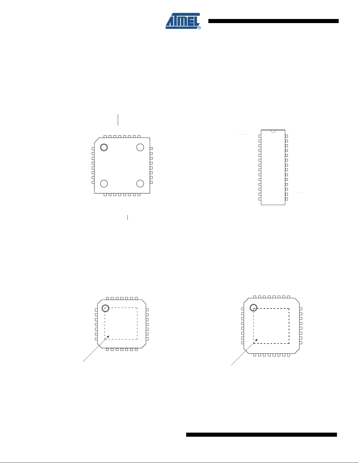
1. Pin Configurations
TQFP Top View
PDIP
9)
8)
)
Figure 1-1. Pinout ATmega48P/88P/168P/328P
PD2 (INT0/PCINT18)
PD1 (TXD/PCINT17)
PD0 (RXD/PCINT16)
PC6 (RESET/PCINT14)
PC5 (ADC5/SCL/PCINT13)
PC4 (ADC4/SDA/PCINT12)
PC3 (ADC3/PCINT11)
PC2 (ADC2/PCINT10)
(PCINT19/OC2B/INT1) PD3
(PCINT20/XCK/T0) PD4
(PCINT6/XTAL1/TOSC1) PB6
(PCINT7/XTAL2/TOSC2) PB7
GND
VCC
GND
VCC
32313029282726
1
2
3
4
5
6
7
8
9101112131415
25
24
23
22
21
20
19
18
17
16
PC1 (ADC1/PCINT9)
PC0 (ADC0/PCINT8)
ADC7
GND
AREF
ADC6
AVCC
PB5 (SCK/PCINT5)
(PCINT14/RESET) PC6
(PCINT16/RXD) PD0
(PCINT17/TXD) PD1
(PCINT18/INT0) PD2
(PCINT19/OC2B/INT1) PD3
(PCINT20/XCK/T0) PD4
(PCINT6/XTAL1/TOSC1) PB6
(PCINT7/XTAL2/TOSC2) PB7
(PCINT21/OC0B/T1) PD5
(PCINT22/OC0A/AIN0) PD6
(PCINT0/CLKO/ICP1) PB0
VCC
GND
(PCINT23/AIN1) PD7
1
2
3
4
5
6
7
8
9
10
11
12
13
14
28
PC5 (ADC5/SCL/PCINT13)
27
PC4 (ADC4/SDA/PCINT12)
26
PC3 (ADC3/PCINT11)
25
PC2 (ADC2/PCINT10)
24
PC1 (ADC1/PCINT9)
23
PC0 (ADC0/PCINT8)
22
GND
21
AREF
20
AVCC
19
PB5 (SCK/PCINT5)
18
PB4 (MISO/PCINT4)
17
PB3 (MOSI/OC2A/PCINT3)
16
PB2 (SS/OC1B/PCINT2)
15
PB1 (OC1A/PCINT1)
(PCINT19/OC2B/INT1) PD3
(PCINT20/XCK/T0) PD4
VCC
GND
(PCINT6/XTAL1/TOSC1) PB6
(PCINT7/XTAL2/TOSC2) PB7
(PCINT21/OC0B/T1) PD5
NOTE: Bottom pad should be soldered to ground.
(PCINT1/OC1A) PB1
(PCINT23/AIN1) PD7
(PCINT21/OC0B/T1) PD5
(PCINT0/CLKO/ICP1) PB0
(PCINT22/OC0A/AIN0) PD6
28 MLF Top View
PD2 (INT0/PCINT18)
PD1 (TXD/PCINT17)
PD0 (RXD/PCINT16)
PC6 (RESET/PCINT14)
PC5 (ADC5/SCL/PCINT13)
28272625242322
1
2
3
4
5
6
7
891011121314
(PCINT1/OC1A) PB1
(PCINT23/AIN1) PD7
(PCINT2/SS/OC1B) PB2
(PCINT0/CLKO/ICP1) PB0
(PCINT22/OC0A/AIN0) PD6
(PCINT4/MISO) PB4
(PCINT2/SS/OC1B) PB2
(PCINT3/OC2A/MOSI) PB3
PC4 (ADC4/SDA/PCINT12)
PC3 (ADC3/PCINT11)
PC2 (ADC2/PCINT10)
21
PC1 (ADC1/PCINT9)
20
PC0 (ADC0/PCINT8)
19
GND
18
AREF
17
AVCC
16
PB5 (SCK/PCINT5)
15
(PCINT4/MISO) PB4
(PCINT3/OC2A/MOSI) PB3
(PCINT19/OC2B/INT1) PD3
(PCINT20/XCK/T0) PD4
(PCINT6/XTAL1/TOSC1) PB6
(PCINT7/XTAL2/TOSC2) PB7
NOTE: Bottom pad should be soldered to ground.
GND
VCC
GND
VCC
1
2
3
4
5
6
7
8
32 MLF Top View
PD2 (INT0/PCINT18)
PD1 (TXD/PCINT17)
PD0 (RXD/PCINT16)
PC6 (RESET/PCINT14)
PC5 (ADC5/SCL/PCINT13)
PC4 (ADC4/SDA/PCINT12)
PC3 (ADC3/PCINT11)
32313029282726
9101112131415
(PCINT1/OC1A) PB1
(PCINT23/AIN1) PD7
(PCINT21/OC0B/T1) PD5
PCINT22/OC0A/AIN0) PD6
(PCINT2/SS/OC1B) PB2
(PCINT0/CLKO/ICP1) PB0
(PCINT3/OC2A/MOSI) PB3
PC2 (ADC2/PCINT10)
25
PC1 (ADC1/PCINT
24
PC0 (ADC0/PCINT
23
ADC7
22
GND
21
AREF
20
ADC6
19
AVCC
18
PB5 (SCK/PCINT5
17
16
(PCINT4/MISO) PB4
2
8025D–AVR–03/08

1.1 Pin Descriptions
1.1.1 VCC
Digital supply voltage.
1.1.2 GND
Ground.
1.1.3 Port B (PB7:0) XTAL1/XTAL2/TOSC1/TOSC2
Port B is an 8-bit bi-directional I/O port with internal pull-up resistors (selected for each bit). The
Port B output buffers have symmetrical drive characteristics with both high sink and source
capability. As inputs, Port B pins that are externally pulled low will source current if the pull-up
resistors are activated. The Port B pins are tri-stated when a reset co ndition becomes active,
even if the clock is not running.
Depending on the clock selection fuse settings, PB6 can be used as input to the inverting Oscillator amplifier and input to the internal clock oper ating circuit.
Depending on the clock selection fuse settings, PB7 can be used as output from the inverting
Oscillator amplifier.
ATmega48P/88P/168P/328P
1.1.4 Port C (PC5:0)
1.1.5 PC6/RESET
If the Internal Calibrated RC Oscillator is used as chip clock source, PB7..6 is used as TOSC2..1
input for the Asynchronous Timer/Counter2 if the AS2 bit in ASSR is set.
The various special features of Port B are elaborated in ”Alternate Functions of Port B” on page
83 and ”System Clock and Clock Options” on page 27.
Port C is a 7-bit bi-directional I/O port with internal pull-up resistors (selected for each bit). The
PC5..0 output buffers have symmetrical drive characteristics with both high sink and source
capability. As inputs, Port C pins that are externally pulled low will source current if the pull-up
resistors are activated. The Port C pins are tri-stated when a reset condition becomes active,
even if the clock is not running.
If the RSTDISBL Fuse is programmed, PC6 is used as an I/O pin. Note that the electrical characteristics of PC6 differ from those of the other pins of Port C.
If the RSTDISBL Fuse is unprogrammed, PC6 is used as a Reset input. A low level on this pin
for longer than the minimum pulse length will generate a Reset, even if the clock is not running.
The minimum pulse length is given in Table 28-3 on page 319. Shorter pulses are not guaranteed to generate a Reset.
The various special features of Port C are elaborated in ”Alternate Functions of Port C” on page
86.
1.1.6 Port D (PD7:0)
8025D–AVR–03/08
Port D is an 8-bit bi-directional I/O port with internal pull-up resistors (selected for each bit). The
Port D output buffers have symmetrical drive characteristics with both high sink and source
capability. As inputs, Port D pins that are externally pulled low will source current if the pull-up
resistors are activated. The Port D pins are tri-stated when a reset condition becomes active,
even if the clock is not running.
3

ATmega48P/88P/168P/328P
The various special features of Port D are elaborated in ”Alternate Functions of Port D” on page
89.
1.1.7 AV
CC
AVCC is the supply voltage pin for the A/D Conver ter, PC3:0 , and ADC7:6. It should be extern ally
connected to V
, even if the ADC is not used. If the ADC is used, it should be co nnecte d to V
CC
through a low-pass filter. Note that PC6..4 use digital supply voltage, VCC.
1.1.8 AREF
AREF is the analog reference pin for the A/D Converter.
1.1.9 ADC7:6 (TQFP and QFN/MLF Package Only)
In the TQFP and QFN/MLF package, ADC7:6 serve as analog inputs to the A/D converter.
These pins are powered from the analog supply and serve as 10-bit ADC channels.
1.2 Disclaimer
Typical values contained in this datasheet are based on simulations and characterization of
other AVR microcontrollers manufactured o n th e same proce ss te ch nolo gy. Min a nd Ma x valu es
will be available after the device is characterized.
CC
4
8025D–AVR–03/08
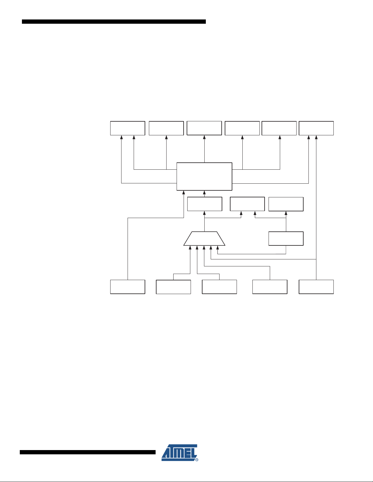
2. Overview
2.1 Block Diagram
ATmega48P/88P/168P/328P
The ATmega48P/88P/168P/328P is a low-power CMOS 8-bit microcontroller based on the AVR
enhanced RISC architecture. By executing powerful instructions in a single clock cycle, the
ATmega48P/88P/168P/328P achieves throughputs approaching 1 MIPS per MHz allowing the
system designer to optimize power consumption versus processing speed.
Figure 2-1. Block Diagram
Comp.
VCC
debugWIRE
PROGRAM
CPU
Internal
Bandgap
LOGIC
SRAMFlash
AVC C
AREF
GND
2
6
GND
Watchdog
Timer
Watchdog
Oscillator
Oscillator
Circuits /
Clock
Generation
EEPROM
8bit T/C 2
DATA B US
Powe r
Supervision
POR / BOD &
RESET
16bit T/C 18bit T/C 0 A/D Conv.
Analog
8025D–AVR–03/08
USART 0
SPI TWI
PORT C (7)PORT B (8)PORT D (8)
RESET
XTAL[1..2]
ADC[6..7]PC[0..6]PB[0..7]PD[0..7]
The AVR core combines a rich instruction set with 32 general purpose working registers. All the
32 registers are directly connected to the Arithmetic Logic Unit (ALU), allowing two independent
registers to be accessed in one single instruction executed in one clock cycle. The resulting
5

ATmega48P/88P/168P/328P
architecture is more code efficient while achieving throughputs up to ten times faster than conventional CISC microcontrollers.
The ATmega48P/88P/168P/328P provides the following features: 4K/8K/16K/32K bytes of InSystem Programmable Flash with Read-While-Write capabilities, 256/512/512/1K bytes
EEPROM, 512/1K/1K/2K bytes SRAM, 23 general purpose I/O lines, 32 general purpose working registers, three flexible Timer/C ounters with compare modes, inter nal and external
interrupts, a serial programmable USART, a byte-oriented 2-wire Serial Interface, an SPI serial
port, a 6-channel 10-bit ADC (8 channels in TQFP and QFN/MLF packages), a programmable
Watchdog Timer with internal Oscillator, and five software selectable power saving modes. The
Idle mode stops the CPU while allowing the SRAM, Timer/Counters, USART, 2-wire Serial Interface, SPI port, and interrupt system to continue func tioning. The Power- down mode saves th e
register contents but freezes the Oscillator, disabling all other chip functions until the next interrupt or hardware reset. In Power-save mo de, the asynchronous timer continues to run, allowing
the user to maintain a timer base while the rest of the device is sleeping. The ADC Noise Re duction mode stops the CPU and all I/O modules except asynchronous timer and ADC, to minimize
switching noise during ADC conversions. In Standby mode, the crystal/resonator Oscillator is
running while the rest of the device is sleeping. This allows v ery fast start-up combined with low
power consumption.
The device is manufactured using Atmel’s high density non-volatile memory technology. The
On-chip ISP Flash allows the program memory to be reprogrammed In-System through an SPI
serial interface, by a conventional non-volatile memory programmer, or by an On-chip Boot program running on the AVR core. The Boot program can use any interface to download the
application program in the Application Flash memory. Software in the Boot Flash section will
continue to run while the Application Flash section is updated, providing true Read-While-Write
operation. By combining an 8-bit RISC CPU with In-System Self-Programmable Flash on a
monolithic chip, the Atmel ATmega48P/88P/168P/328P is a powerful microcontroller that provides a highly flexible and cost effective solution to many embedded control applications.
The ATmega48P/88P/168P/328P AVR is supported with a full suite of program and system
development tools including: C Compilers, Macro Assemblers, Program Debugger/Simulators,
In-Circuit Emulators, and Evaluation kits.
2.2 Comparison Between ATmega48P, ATmega88P, ATmega168P, and ATmega328P
The ATmega48P, ATmega88P, ATmega168P, and ATmega328P differ only in memory sizes,
boot loader support, and interrupt vector sizes. Table 2-1 summarizes the different memory and
interrupt vector sizes for the three devices.
Table 2-1. Memory Size Summary
Device Flash EEPROM RAM Interrupt Vector Size
ATmega48P 4K Bytes 256 Bytes 512 Bytes 1 instruction word/vector
ATmega88P 8K Bytes 512 Bytes 1K Bytes 1 instruction word/vector
ATmega168P 16K Bytes 512 Bytes 1K Bytes 2 instruction words/vector
ATmega328P 32K Bytes 1K Bytes 2K Bytes 2 instructions words/vector
ATmega88P, ATmega168P, and ATmega328P support a real Read-While-Write Self-Programming mechanism. There is a separate Boot Loader Section, and the SPM instruction can only
execute from there. In ATmega48P, there is no Read-While-Write suppor t and no se pa rate Boot
Loader Section. The SPM instruction can execute from the ent ire Flash.
6
8025D–AVR–03/08

3. Resources
ATmega48P/88P/168P/328P
A comprehensive set of development tools, application notes and datasheets are available for
download on http://www.atmel.com/avr.
8025D–AVR–03/08
7

ATmega48P/88P/168P/328P
Note: 1.
4. Data Retention
Reliability Qualification results show that the projected data retention failure rate is much less
than 1 PPM over 20 years at 85°C or 100 years at 25°C.
5. About Code Examples
This documentation contains simple code examples t hat brief ly show h ow to us e various parts of
the device. These code examples assume that the part specific header file is included b efore
compilation. Be aware that not all C compiler vendors include bit definitions in the header files
and interrupt handling in C is compiler dependent . Please con firm wit h the C com piler d ocume ntation for more details.
For I/O Registers located in extended I/O map, “IN”, “OUT”, “SBIS”, “SBIC”, “CBI”, and “SBI”
instructions must be replaced with instructions that allow access to extended I/O. Typically
“LDS” and “STS” combined with “SBRS”, “SBRC”, “SBR”, and “CBR”.
8
8025D–AVR–03/08
6. AVR CPU Core
6.1 Overview
ATmega48P/88P/168P/328P
This section discusses the AVR core architecture in general. The main function of the CPU core
is to ensure correct program execution. The CPU must therefore be able to access memories,
perform calculations, control peripherals, and handle interrupts.
Figure 6-1. Block Diagram of the AVR Architecture
Data Bus 8-bit
Flash
Program
Memory
Instruction
Register
Instruction
Decoder
Control Lines
Program
Counter
Direct Addressing
Indirect Addressing
Status
and Control
32 x 8
General
Purpose
Registrers
ALU
Data
SRAM
EEPROM
Interrupt
Unit
SPI
Unit
Watchdog
Timer
Analog
Comparator
I/O Module1
I/O Module 2
I/O Module n
8025D–AVR–03/08
I/O Lines
In order to maximize performance and parallelism, the AVR uses a Harvard architecture – with
separate memories and buses for program and data. Instructions in the program memory are
executed with a single level pipelining. While one instruction is being executed, the next instruction is pre-fetched from the program memory. This concept enables instructions to be executed
in every clock cycle. The program memory is In-System Reprogrammable Flash memory.
The fast-access Register File contains 32 x 8-bit general purpose working registers with a single
clock cycle access time. This allows single-cycle Arithmetic Logic Unit (ALU) operation. In a typ-
9

ATmega48P/88P/168P/328P
ical ALU operation, two operands are output from the Register File, the operation is executed,
and the result is stored back in the Register File – in one clock cycle.
Six of the 32 registers can be used as three 16-bit indirect address register pointers for Data
Space addressing – enabling efficient address calculations. One of the these address pointe rs
can also be used as an address pointe r for look up tables in Flash pr ogram memory. Thes e
added function registers are the 16-bit X-, Y-, and Z-register, described later in this section.
The ALU supports arithmetic and logic operations between registers or between a constant and
a register. Single register operations can also be executed in the AL U. After an arith metic operation, the Status Register is updated to reflect informat ion about the result of the operation.
Program flow is provided by conditional and unconditional jump and call instructions, able to
directly address the whole address space. Most AVR instructions have a single 16-bit word format. Every program memory address contains a 16- or 32-bit instruction.
Program Flash memory space is divided in two sections, the Boot Program section and the
Application Program section. Both sections have dedicated Lock bits for write and read/write
protection. The SPM instruction that writes into the Application Flash memory section must
reside in the Boot Program section.
During interrupts and subroutine calls, the return address Prog ram Counter (PC) is stored on the
Stack. The Stack is effectively allocated in the general data SRAM, and consequently the Stack
size is only limited by the total SRAM size and the usage of the SRAM. All user programs must
initialize the SP in the Reset routine (before subroutines or interrupts are executed). The Stack
Pointer (SP) is read/write accessible in the I/O space. The data SRAM can easily be accessed
through the five different addressing modes supported in the AVR architecture.
The memory spaces in the AVR architecture are all linear and regular memory maps.
A flexible interrupt module has its control registers in the I/O space with an additional Global
Interrupt Enable bit in the Status Register. All interrupts have a separate Interrupt Vector in the
Interrupt Vector table. The interrupts have priority in accordance with their Interrupt Vector position. The lower the Interrupt Vector address, the higher the priority.
The I/O memory space contains 64 addresses for CPU peripheral functions as Control Registers, SPI, and other I/O functions. The I/O Memory can be acces sed directly, or as the Data
Space locations following those of the Register File, 0x20 - 0x5F. In addition, the
ATmega48P/88P/168P/328P has Extended I/O space from 0x60 - 0xFF in SRAM where only
the ST/STS/STD and LD/LDS/LDD instructions can be used.
6.2 ALU – Arithmetic Logic Unit
The high-performance AVR ALU operates in direct connection with all the 32 general purpose
working registers. Within a single clock cycle, arithmetic operations between general purpose
registers or between a register and an immediate are execut ed . The ALU ope ra tio ns are divided
into three main categories – arithmetic, logical, and bit-functions. Some implementations of the
architecture also provide a powerful multiplier supporting both signed/unsigned multiplication
and fractional format. See the “Instruction Set” section for a detailed description.
6.3 Status Register
The Status Register contains information about the result of the most recently executed arithmetic instruction. This information can be used for altering program flow in order to perform
conditional operations. Note that the Status Register is updated after all ALU operations, as
10
8025D–AVR–03/08

specified in the Instruction Set Refe rence. This wil l in many cases remove the n eed for using the
dedicated compare instructions, resulting in faster and more compact code.
The Status Register is not automatically stored when entering an interrupt routine and restored
when returning from an interrupt. This must be hand le d by so ftware.
6.3.1 SREG – AVR Status Register
The AVR Status Register – SREG – is defined as:
Bit 76543210
0x3F (0x5F) I T H S V N Z C SREG
Read/Write R/W R/W R/W R/W R/W R/W R/W R/W
Initial Value 0 0 0 0 0 0 0 0
• Bit 7 – I: Global Interrupt Enable
The Global Interrupt Enable bit must be set for the interrupts to be enabled. The individual interrupt enable control is then performed in separate control registers. If the Global Interrupt Enable
Register is cleared, none of the interrupts are enabled independent of the individual interrupt
enable settings. The I-bit is cleared by hardware after an interrupt has occurred, and is set by
the RETI instruction to enable subsequent interrupts. The I-bit can also be set and cleared by
the application with the SEI and CLI instructions, as described in the instruction set reference.
ATmega48P/88P/168P/328P
• Bit 6 – T: Bit Copy Storage
The Bit Copy instructions BLD (Bit LoaD) and BST (Bit STore) use the T-bit as source or destination for the operated bit. A bit from a register in the Register File can be copied into T by the
BST instruction, and a bit in T can be copied into a bit in a register in the Register File by the
BLD instruction.
• Bit 5 – H: Half Carry Flag
The Half Carry Flag H indicates a Half Carry in some arithmetic operations. Half Carry Is useful
in BCD arithmetic. See the “Instruction Set Description” for detailed information.
• Bit 4 – S: Sign Bit, S = N
⊕ V
The S-bit is always an exclusive or between the Negative Flag N and the Two’s Complement
Overflow Flag V. See the “Instruction Set Description” for detailed information.
• Bit 3 – V: Two’s Complement Overflow Flag
The Two’s Complement Overflow Flag V supports two’s complement arithmetics. See the
“Instruction Set Description” for detailed information.
• Bit 2 – N: Negative Flag
The Negative Flag N indicates a negative result in an arithmetic or logic operation. See the
“Instruction Set Description” for detailed information.
• Bit 1 – Z: Zero Flag
The Zero Flag Z indicates a zero result in an arithmetic or logic operation. See the “Instruction
Set Description” for detailed information.
8025D–AVR–03/08
• Bit 0 – C: Carry Flag
The Carry Flag C indicates a carry in an arithmetic or logic operation. See the “Instruction Set
Description” for detailed information.
11

ATmega48P/88P/168P/328P
6.4 General Purpose Register File
The Register File is optimized for the AVR Enhanced RISC instruction set. In order t o achieve
the required performance and flexibility, the following input/output schemes are supported by the
Register File:
• One 8-bit output operand and one 8-bit result input
• Two 8-bit output operands and one 8-bit result input
• Two 8-bit output operands and one 16-bit result input
• One 16-bit output operand and one 16-bit result input
Figure 6-2 shows the structure of the 32 general purpose working registers in the CPU.
Figure 6-2. AVR CPU General Purpose Working Registers
General R14 0x0E
Purpose R15 0x0F
Working R16 0x10
Registers R17 0x11
7 0 Addr.
R0 0x00
R1 0x01
R2 0x02
…
R13 0x0D
…
R26 0x1A X-register Low Byte
R27 0x1B X-register High Byte
R28 0x1C Y-register Low Byte
R29 0x1D Y-register High Byte
R30 0x1E Z-register Low Byte
R31 0x1F Z-register High Byte
12
Most of the instructions operating on the Register File have direct access to all registers, and
most of them are single cycle instructions.
As shown in Figure 6-2, each register is also assigned a data memory address, mapping them
directly into the first 32 locations of the user Data Space. Although not being physically implemented as SRAM locations, this memory organization provides great flexibility in access of the
registers, as the X-, Y- and Z-pointer registers can be set to index any register in the file.
8025D–AVR–03/08
6.4.1 The X-register, Y-register, and Z-register
The registers R26..R31 have some added functions to their general purpose usage. These registers are 16-bit address pointers for indirect addressing of the data space. The three indirect
address registers X, Y, and Z are defined as described in Figure 6-3.
Figure 6-3. The X-, Y-, and Z-registers
15 XH XL 0
X-register 707 0
R27 (0x1B) R26 (0x1A)
15 YH YL 0
Y-register 707 0
R29 (0x1D) R28 (0x1C)
15 ZH ZL 0
Z-register 70 7 0
R31 (0x1F) R30 (0x1E)
In the different addressing modes these addr ess regist er s have fun cti ons a s fi xed d isp lacement ,
automatic increment, and automatic decrement (see the instruction set reference for details).
ATmega48P/88P/168P/328P
6.5 Stack Pointer
The Stack is mainly used for storing temporary data, for storing local variables and for storing
return addresses after interrupts and subroutine calls. The Stack Pointer Register always points
to the top of the Stack. Note that the Stack is imp lemented as growing f rom higher memor y locations to lower memory locations. This implies that a Stack PUSH co mmand decr eases th e Stack
Pointer.
The Stack Pointer points to the data SRAM Stack area where the Subroutine and Interrupt
Stacks are located. This Stack space in the data SRAM must be defined by the program before
any subroutine calls are executed or interrupts are enabled. The Stack Pointer must be set to
point above 0x0100, preferably RAMEND. The Stack Pointer is decremented by one when data
is pushed onto the Stack with the PUSH instruction, and it is decremented by two when the
return address is pushed onto the Stack with subroutine call or interrupt. The Stack Pointer is
incremented by one when data is popped from the Stack with the POP instruction , and it is incremented by two when data is popped from the Stack with return from subroutine RET or return
from interrupt RETI.
The AVR Stack Pointer is implemented as two 8-bit registers in the I/O space. The number of
bits actually used is implementation dependent. Note that the data space in some implementations of the AVR architecture is so small that only SPL is needed. In this case, the SPH Register
will not be present.
8025D–AVR–03/08
13
ATmega48P/88P/168P/328P
6.5.1 SPH and SPL – Stack Pointer High and Stack Pointer Low Register
2
R
T1 T2 T3 T4
Bit 151413121110 9 8
0x3E (0x5E) SP15 SP14 SP13 SP12 SP11 SP10 SP9 SP8 SPH
0x3D (0x5D) SP7 SP6 SP5 SP4 SP3 SP2 SP1 SP0 SPL
76543210
Read/Write R/W R/W R/W R/W R/W R/W R/W R/W
R/W R/W R/W R/W R/W R/W R/W R/W
Initial Value
RAMEND RAMEND RAMEND RAMEND RAMEND RAMEND RAMEND RAMEND
RAMEND RAMEND RAMEND RAMEND RAMEND RAMEND RAMEND RAMEND
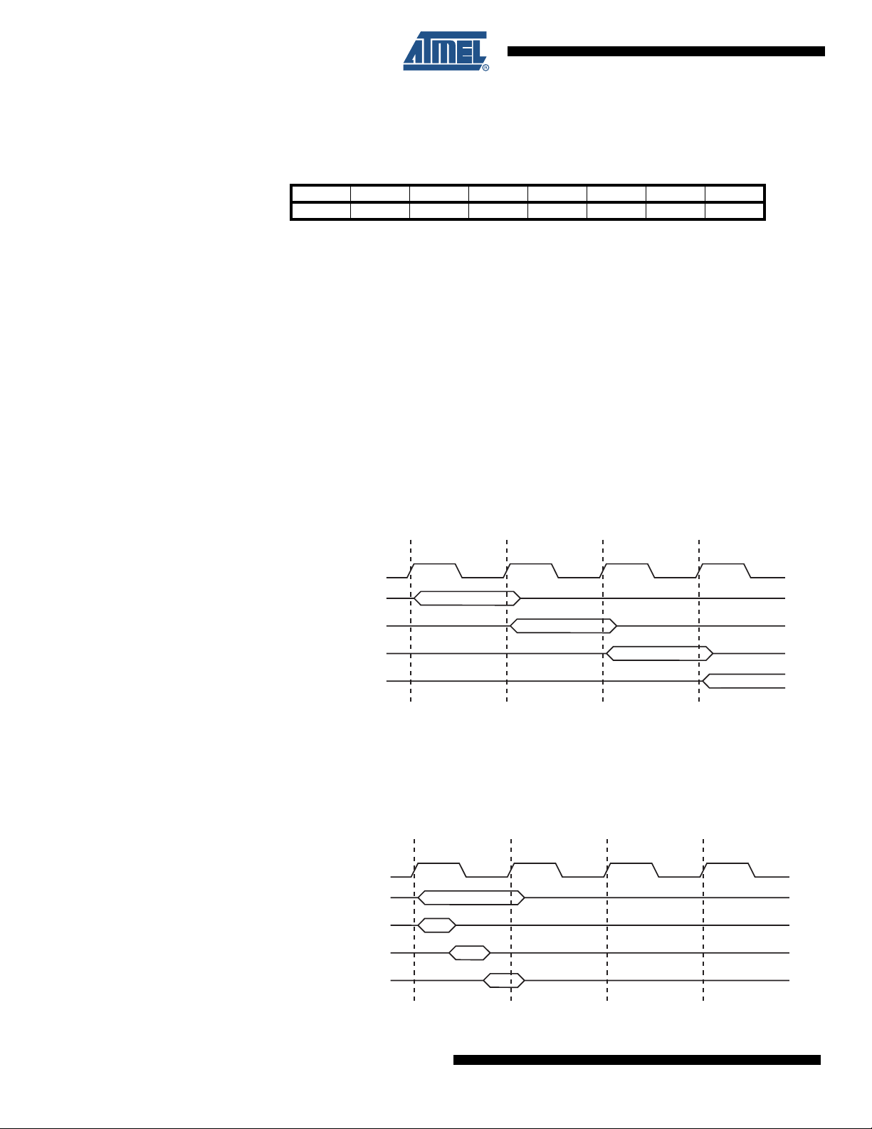
6.6 Instruction Execution Timing
This section describes the general access timing concepts for instruction execution. The AVR
CPU is driven by the CPU clock clk
chip. No internal clock division is used.
Figure 6-4 shows the parallel instruction fetches and instruction executions enabled by the Har-
vard architecture and the fast-access Register File concept. This is the basic pipelining concept
to obtain up to 1 MIPS per MHz with the corresponding unique results for functions per cost,
functions per clocks, and functions per power-unit.
Figure 6-4. The Parallel Instruction Fetches and Instruction Executions
, directly generated from the selected clock source for the
CPU
T1 T2 T3 T4
clk
CPU
1st Instruction Fetch
1st Instruction Execute
2nd Instruction Fetch
nd Instruction Execute
3rd Instruction Fetch
3rd Instruction Execute
4th Instruction Fetch
Figure 6-5 shows the internal timing concept for th e Regi ster File . In a single clock cycl e an ALU
operation using two register operands is executed, and the result is stored back to the destination register.
Figure 6-5. Single Cycle ALU Operation
clk
CPU
Total Execution Time
egister Operands Fetch
ALU Operation Execute
Result Write Back
14
8025D–AVR–03/08

6.7 Reset and Interrupt Handling
The AVR provides several different interrupt sources. These interrupts and the separate Reset
Vector each have a separate program vector in the program memory space. All interrupts are
assigned individual enable bits which must be written logic one toge ther with the Glo bal Interru pt
Enable bit in the Status Register in order to enable the interrupt. Depending on the Program
Counter value, interrupts may be automatically disabled when Boot Lock bits BLB02 or BLB12
are programmed. This feature improves software security. See the section ”Memory Program-
ming” on page 294 for details.
The lowest addresses in the program memory space are by default defined as the Reset and
Interrupt Vectors. The complete list of vectors is shown in ”Interrupts” on page 58. The list also
determines the priority levels of the different interrupts. The lower the address the higher is the
priority level. RESET has the highest priority, and next is INT0 – the External Interrupt Request
0. The Interrupt Vectors can be moved to t he start of the Boot Flash section by setting t he IVSEL
bit in the MCU Control Register (MCUCR). Refer to ”Interrupts” on page 58 for more information.
The Reset Vector can also be moved to the start of the Boot Flash section by programming the
BOOTRST Fuse, see ”Boot Loader Support – Read-While-Write Self-Programming,
ATmega88P, ATmega168P and ATmega328P” on page 278.
When an interrupt occurs, the Global Interrupt Enable I-bit is cleared and all interrupts are disabled. The user software can write logic one to the I-bit to enable nested interrupts. All enabled
interrupts can then interrupt the current interrupt routine. The I-bit is automatically set when a
Return from Interrupt instruction – RETI – is executed.
ATmega48P/88P/168P/328P
There are basically two types of interrupts. The first type is triggered by an event that sets the
Interrupt Flag. For these interrupts, the Program Counter is vectored to the actual Interrupt Vector in order to execute the interrupt handling routine, and hardware clears the corresponding
Interrupt Flag. Interrupt Flags can also be cleared by writing a logic one to the flag bit position(s)
to be cleared. If an interrupt condition occurs while the corresponding interrupt enable bit is
cleared, the Interrupt Flag will be set and remembered until the interrupt is enabled, or the flag is
cleared by software. Similarly, if one or more interrupt conditions occur while the Global Interrupt
Enable bit is cleared, the corresponding Interrupt Flag(s) will be set and remembered until the
Global Interrupt Enable bit is set, and will then be executed by order of priority.
The second type of interrupts will trigger as long as the interrupt condition is present. These
interrupts do not necessarily have Int errupt Flags. If the interrup t condition disappears before t he
interrupt is enabled, the interrupt will not be triggered.
When the AVR exits from an interrupt, it will always return to the main program and execute one
more instruction before any pending interrupt is served.
Note that the Status Register is not automatically stored when entering an interrupt routine, nor
restored when returning from an interrupt rou tine. This must be handled by software.
When using the CLI instruction to disable interrupts, the interrupts will be immediately disabled.
No interrupt will be executed after the CLI instruction, even if it occurs simultaneously with the
CLI instruction. The following example shows how this can be used to avoid interrupts during the
timed EEPROM write sequence.
8025D–AVR–03/08
15

ATmega48P/88P/168P/328P
Assembly Code Example
in r16, SREG ; store SREG value
cli ; disable interrupts during timed sequence
sbi EECR, EEMPE ; start EEPROM write
sbi EECR, EEPE
out SREG, r16 ; restore SREG value (I-bit)
C Code Example
char cSREG;
cSREG = SREG; /* store SREG value */
/* disable interrupts during timed sequence */
_CLI();
EECR |= (1<<EEMPE); /* start EEPROM write */
EECR |= (1<<EEPE);
SREG = cSREG; /* restore SREG value (I-bit) */
When using the SEI instruction to enable interrupts, the instruction following SEI will be executed before any pending interrupts, as shown in this example.
Assembly Code Example
sei ; set Global Interrupt Enable
sleep; enter sleep, waiting for interrupt
; note: will enter sleep before any pending interrupt(s)
C Code Example
__enable_interrupt(); /* set Global Interrupt Enable */
__sleep(); /* enter sleep, waiting for interrupt */
/* note: will enter sleep before any pending interrupt(s) */
6.7.1 Interrupt Response Time
The interrupt execution response for all the enabled AVR interrupts is four clock cycles minimum. After four clock cycles the program vector addre ss fo r t he actua l interr up t ha nd ling rout ine
is executed. During this four clock cycle period, the Program Counter is pushed onto the Stack.
The vector is normally a jump to the interrupt routine, and this jump takes three clock cycles. If
an interrupt occurs during execution of a multi-cycle instruction, this instruction is completed
before the interrupt is served. If an interrupt occurs when the MCU is in sleep mode, the interrupt
execution response time is increased by four clock cycles. This increase comes in ad dition to the
start-up time from the selected sleep mode.
A return from an interrupt handling routine takes four clock cycles. During these four clock
cycles, the Program Counter (two bytes) is popped back from the Stack, the Stack Pointer is
incremented by two, and the I-bit in SREG is set.
16
8025D–AVR–03/08

ATmega48P/88P/168P/328P
7. AVR Memories
7.1 Overview
This section describes the different memories in the ATmega48P/88P/168P/328P. The AVR
architecture has two main memory spaces, the Data Memory and the Program Memory space.
In addition, the ATmega48P/88P/168P/32 8P fe atur es an EEPRO M Memor y for da ta stor ag e. All
three memory spaces are linear and regular.
7.2 In-System Reprogrammable Flash Program Memory
The ATmega48P/88P/168P/328P contains 4/8/16/32K bytes On-chip In-System Reprogrammable Flash memory for program st orage. Since all AVR instruct ions are 16 or 32 bits wid e, the
Flash is organized as 2/4/8/16K x 16. For software security, the Flash Program memory space is
divided into two sections, Boot Loader Section and Application Program Section in ATmega88P
and ATmega168P. ATmega48P does not have separate Boot Loader and Application Program
sections, and the SPM instruction can be executed from the entire Flash. See SELFPRGEN
description in section ”SPMCSR – Store Program Memory Control and Status Register” on page
276 and page 292for more details.
The Flash memory has an endurance of at least 10,000 write/erase cycles. The
ATmega48P/88P/168P/328P Program Counter (PC) is 11/12/13/14 bits wide, thus addressing
the 2/4/8/16K program memory locations. The operation of Boot Program section and associated Boot Lock bits for software protection are described in detail in ”Self-Programming the
Flash, ATmega48P” on page 270 and ”Boot Loader Support – Read-While-Write Self-Programming, ATmega88P, ATmega168P and ATmega328P” on page 278. ”Memory Programming” on
page 294 contains a detailed description on Flash Programming in SPI- or Parallel Programming
mode.
Constant tables can be allocated within the entire program memory address space (see the LPM
– Load Program Memory instruction description).
Timing diagrams for instruction fetch and execution are presented in ”Instruction Execution Tim-
ing” on page 14.
8025D–AVR–03/08
17

ATmega48P/88P/168P/328P
Figure 7-1. Program Memory Map, ATmega48 P
F
Program Memory
Application Flash Section
0x0000
0x7FF
Figure 7-2. Program Memory Map, ATmega88P, ATmega168P, and ATmega328P
Program Memory
0x0000
Application Flash Section
Boot Flash Section
0x0FFF/0x1FFF/0x3FF
18
8025D–AVR–03/08

7.3 SRAM Data Memory
F
Figure 7-3 shows how the ATmega48P/88P/168P/328P SRAM Memory is organized.
The ATmega48P/88P/168P/328P is a complex microcontroller with more peripheral units than
can be supported within the 64 locations reserved in the Opcode for the IN and OUT instructions. For the Extended I/O space from 0x60 - 0xFF in SRAM, only the ST/STS/STD and
LD/LDS/LDD instructions can be used.
The lower 768/1280/1280/2303 data memory locations address both the Register File, the I/O
memory, Extended I/O memory, and the internal data SRAM. The first 32 locations address the
Register File, the next 64 location the standard I/O memory, then 160 locations of Extended I/O
memory, and the next 512/1024/1024/ 2048 locations address the internal data SRAM.
The five different addressing modes for the data memory cover: Direct, Indirect with Displacement, Indirect, Indirect with Pre-decrement, and Indirect with Post-increment. In the Register
File, registers R26 to R31 feature the indirect addressing pointer registers.
The direct addressing reaches the entire data space.
The Indirect with Displacement mode reaches 63 address locations f rom the base address given
by the Y- or Z-register.
ATmega48P/88P/168P/328P
When using register indirect addressing modes with automatic pre-decrement and post-increment, the address registers X, Y, and Z are decremented or incremented.
The 32 general purpose working registers, 64 I/O Registers, 160 Extended I/O Registers, and
the 512/1024/1024/2048 bytes of in t ernal d at a SRAM in th e ATme ga4 8P/88 P/1 68P/ 328P ar e a ll
accessible through all these addressing modes. The Register File is described in ”General Pur-
pose Register File” on page 12.
Figure 7-3. Data Memory Map
Data Memory
32 Registers
64 I/O Registers
160 Ext I/O Reg.
Internal SRAM
(512/1024/1024/2048 x 8)
0x0000 - 0x001F
0x0020 - 0x005F
0x0060 - 0x00FF
0x0100
0x02FF/0x04FF/0x04FF/0x08F
8025D–AVR–03/08
19

ATmega48P/88P/168P/328P
7.3.1 Data Memory Access Times
A
This section describes the general access timing concepts for internal memory access. The
internal data SRAM access is performed in two clk
Figure 7-4. On-chip Data SRAM Access Cycles
clk
CPU
ddress
Data
cycles as described in Figure 7-4.
CPU
T1 T2 T3
Compute Address
Address valid
7.4 EEPROM Data Memory
The ATmega48P/88P/168P/328P contains 256/512/512/1K bytes of data EEPROM memory. It
is organized as a separate data space, in which single bytes can be read and written. The
EEPROM has an endurance of at least 100,000 write/erase cycles. The access between the
EEPROM and the CPU is described in the following, specifying the EEPROM Address Registers, the EEPROM Data Register, and the EEPROM Control Register.
”Memory Programming” on page 294 contains a detailed description on EEPROM Programming
in SPI or Parallel Programming mode.
7.4.1 EEPROM Read/Write Access
The EEPROM Access Registers are accessible in the I/O space.
WR
Data
RD
Memory Access Instruction
Write
Read
Next Instruction
The write access time for the EEPROM is given in Table 7-2. A self-timing function, however,
lets the user software detect when the next byte can be written. If the user code contains instructions that write the EEPROM, some precautions must be taken. In heavily filtered power
supplies, V
is likely to rise or fall slowly on power-up/down. This causes the device for some
CC
period of time to run at a voltage lower than specif ied as mi nimum for the clock fre quen cy used .
See ”Preventing EEPROM Corruption” on page 21 for details on how to avoid problems in these
situations.
In order to prevent unintentional EEPROM writes, a specific write procedure must be followed.
Refer to the description of the EEPROM Control Register for details on this.
When the EEPROM is read, the CPU is halted for four clock cycles before the next instruction is
executed. When the EEPROM is written, the CPU is halted for two clock cycles before the next
instruction is executed.
20
8025D–AVR–03/08

7.4.2 Preventing EEPROM Corruption
During periods of low V
too low for the CPU and the EEPROM to operate properly. These issues a re the same as for
board level systems using EEPROM, and the same design solutions should be applied.
An EEPROM data corruption can be caused by two situations when the voltage is too low. First,
a regular write sequence to the EEPROM requires a minimum voltage to operate correctly. Secondly, the CPU itself can execute instructions incorrectly, if the supply voltage is too low.
EEPROM data corruption can easily be avoided by following this design recommendation:
Keep the AVR RESET active (low) during periods of insufficient power supply voltage. This can
be done by enabling the internal Brown-out Detector (BOD). If the detection level of the internal
BOD does not match the needed detection level, an exter nal low V
be used. If a reset occurs while a write operation is in progress, the write operation will be completed provided that the power supply voltage is sufficient.
7.5 I/O Memory
The I/O space definition of the ATmega48P/88P/168P/328P is shown in ”Register Summary” on
page 400.
All ATmega48P/88P/168P/328P I/Os and peripherals are placed in the I/O space. All I/O locations may be accessed by the LD/LDS/LDD and ST/STS/STD instructions, transferring data
between the 32 general purpose working registers and the I/O space. I/O Registers within the
address range 0x00 - 0x1F are directly bit-accessible using the SBI and CBI instructions. In
these registers, the value of single bits can be checked by using the SBIS and SBIC instructions.
Refer to the instruction set section for more details. When using the I/O spe cific commands IN
and OUT, the I/O addresses 0x00 - 0x3F must be used . When addressing I/O Registers as data
space using LD and ST instructions, 0x20 must be added to these addresses. The
ATmega48P/88P/168P/328P is a complex microcontroller with more peripheral units than can
be supported within the 64 location reserved in Opcode for the IN and OUT instructions. For the
Extended I/O space from 0x60 - 0xFF in SRAM, only the ST/STS/STD and LD/LDS/LDD instructions can be used.
ATmega48P/88P/168P/328P
the EEPROM data can be corrupted because the supply voltage is
CC,
reset Protection circuit can
CC
For compatibility with future devices, reserved bits should be written to zero if accessed.
Reserved I/O memory addresses should never be written.
Some of the Status Flags are cleared by writing a logical one to them. Note that, unlike most
other AVRs, the CBI and SBI instructions will only operate on the specified bit, and can therefore
be used on registers containing such Status Flags. The CBI and SBI instructions work with registers 0x00 to 0x1F only.
The I/O and peripherals control registers are explained in later sections.
7.5.1 General Purpose I/O Registers
The ATmega48P/88P/168P/328P contains three General Purpose I/O Registers. These registers can be used for storing any information, and they are particularly useful for storing global
variables and Status Flags. General Purpose I/O Registers within the address range 0x00 0x1F are directly bit-accessible using the SBI, CBI, SBIS, and SBIC instructions.
8025D–AVR–03/08
21

ATmega48P/88P/168P/328P
7.6 Register Description
7.6.1 EEARH and EEARL – The EEPROM Address Register
Bit 1514131211109 8
0x22 (0x42) – – – – – – – EEAR8 EEARH
0x21 (0x41) EEAR7 EEAR6 EEAR5 EEAR4 EEAR3 EEAR2 EEAR1 EEAR0 EEARL
76543210
Read/Write RRRRRRRR/W
R/W R/W R/W R/W R/W R/W R/W R/W
Initial Value 0 0 0 0 0 0 0 X
XXXXXXXX
• Bits 15..9 – Res: Reserved Bits
These bits are reserved bits in the ATmega48P/88P/168P/328P and will always read as zero.
• Bits 8..0 – EEAR8..0: EEPROM Address
The EEPROM Address Registers – EEARH and EEARL specify the EEPROM address in the
256/512/512/1K bytes EEPROM space. The EEPROM data bytes are addressed linearly
between 0 and 255/511/511/1023. The initial value of EEAR is undefined. A proper value must
be written before the EEPROM may be accessed.
EEAR8 is an unused bit in ATmega48P and must always be written to zero.
7.6.2 EEDR – The EEPROM Data Register
Bit 76543210
0x20 (0x40) MSB LSB EEDR
Read/Write R/W R/W R/W R/W R/W R/W R/W R/W
Initial Value 0 0 0 0 0 0 0 0
• Bits 7..0 – EEDR7.0: EEPROM Data
For the EEPROM write operation, the EEDR Register contains the data to b e written to the
EEPROM in the address given by the EEAR Register. For the EEPROM read operation, the
EEDR contains the data read out from the EEPROM at the address given by EEAR.
7.6.3 EECR – The EEPROM Control Register
Bit 76543210
0x1F (0x3F) – – EEPM1 EEPM0 EERIE EEMPE EEPE EERE EECR
Read/Write R R R/W R/W R/W R/W R/W R/W
Initial Value 0 0 X X 0 0 X 0
• Bits 7..6 – Res: Reserved Bits
These bits are reserved bits in the ATmega48P/88P/168P/328P and will always read as zero.
• Bits 5, 4 – EEPM1 and EEPM0: EEPROM Programming Mode Bits
The EEPROM Programming mode bit setting defines which programming action that will be triggered when writing EEPE. It is possible to program data in one atomic operation (erase the old
value and program the new value) or to split the Erase and Write operations in two different
operations. The Programming t imes fo r the d ifferen t modes ar e shown in Table 7- 1. While EEPE
22
8025D–AVR–03/08

ATmega48P/88P/168P/328P
is set, any write to EEPMn will be ignored. During reset, the EEPMn bits will be reset to 0b00
unless the EEPROM is busy programming.
Table 7-1. EEPROM Mode Bits
Programming
EEPM1 EEPM0
0 0 3.4 ms Erase and Write in one operation (Atomic Operation)
0 1 1.8 ms Erase Only
1 0 1.8 ms Write Only
1 1 – Reserved for future use
• Bit 3 – EERIE: EEPROM Ready Interrupt Enable
Writing EERIE to one enables the EEPROM Ready Interrupt if the I bit in SREG is set. Writing
EERIE to zero disables the interrupt. The EEPROM Ready interrupt generates a constant interrupt when EEPE is cleared. The interrupt will not be generated during EEPROM write or SPM.
• Bit 2 – EEMPE: EEPROM Master Write Enable
The EEMPE bit determines whether setting EEPE to one causes the EEPROM to be written.
When EEMPE is set, setting EEPE within four clock cycles will write data to the EEPROM at the
selected address If EEMPE is zero, setting EEPE will have no effect. When EEMPE has been
written to one by software, hardware clears the bit to zero after four clock cycles. See the
description of the EEPE bit for an EEPROM write procedure.
Time Operation
• Bit 1 – EEPE: EEPROM Write Enable
The EEPROM Write Enable Signal EEPE is the write strobe to the EEPROM. When address
and data are correctly set up, the EEPE bit must be written to one to write the value into the
EEPROM. The EEMPE bit must be written to one before a logical one is written to EEPE, otherwise no EEPROM write takes place. The following procedure should be followed when writing
the EEPROM (the order of steps 3 and 4 is not essential):
1. Wait until EEPE becomes zero.
2. Wait until SELFPRGEN in SPMCSR becomes zero.
3. Write new EEPROM address to EEAR (optional).
4. Write new EEPROM data to EEDR (optional).
5. Write a logical one to the EEMPE bit while writing a zero to EEPE in EECR.
6. Within four clock cycles after setting EEMPE, write a logical one to EEPE.
The EEPROM can not be programmed during a CPU write to the Flash memory. The software
must check that the Flash programming is completed before initiating a new EEPROM write.
Step 2 is only relevant if the software contains a Boot Loader allowing the CPU to program the
Flash. If the Flash is never bein g up da te d by th e CPU, step 2 can be omitted. See ”Boot Loader
Support – Read-While-Write Self-Programming, ATmega88P, ATmega168P and ATmega328P”
on page 278 for details about Boot programming.
Caution: An interrupt between step 5 and step 6 will make the write cycle fail, since the
EEPROM Master Write Enable will time-out. If an interrupt routine accessing the EEPROM is
interrupting another EEPROM access, the EEAR or EEDR Register will be modified, causing the
interrupted EEPROM access to fail. It is recommended to have the Global Interrupt Flag cleared
during all the steps to avoid these problems.
8025D–AVR–03/08
23

ATmega48P/88P/168P/328P
When the write access time has elapsed, the EEPE bit is cleared by hardware. The user software can poll this bit and wait for a zero before writing the next byte. When EEPE has been set,
the CPU is halted for two cycles before the next instruction is executed.
• Bit 0 – EERE: EEPROM Read Enable
The EEPROM Read Enable Signal EERE is the read strobe to the EEPROM. When the correct
address is set up in the EEAR Registe r, the EERE b it must be writte n to a log ic one t o trigger t he
EEPROM read. The EEPROM read access takes one instruction, and the requested data is
available immediately. When the EEPROM is read, the CPU is halted for four cycles before the
next instruction is executed.
The user should poll the EEPE bit before starting the read operation. If a write operation is in
progress, it is neither possible to read the EEPROM, nor to change the EEAR Register.
The calibrated Oscillator is used to time the EEPROM accesses. Table 7-2 lists the typica l programming time for EEPROM access from the CPU.
Table 7-2. EEPROM Programming Time
Symbol Number of Calibrated RC Oscillator Cycles Typ Programming Time
EEPROM write
(from CPU)
The following code examples show one assembly and one C function for writing to the
EEPROM. The examples assume that interrupts are controlled (e.g. by disabling interrupts globally) so that no interrupts will occur during execution of these functions. The examples also
assume that no Flash Boot Loader is present in the software. If such code is present, the
EEPROM write function must also wait for any ongoing SPM command to finish.
26,368 3.3 ms
24
8025D–AVR–03/08

ATmega48P/88P/168P/328P
Assembly Code Example
EEPROM_write:
; Wait for completion of previous write
sbic EECR,EEPE
rjmp EEPROM_write
; Set up address (r18:r17) in address register
out EEARH, r18
out EEARL, r17
; Write data (r16) to Data Register
out EEDR,r16
; Write logical one to EEMPE
sbi EECR,EEMPE
; Start eeprom write by setting EEPE
sbi EECR,EEPE
ret
C Code Example
void EEPROM_write(unsigned int uiAddress, unsigned char ucData)
{
/* Wait for completion of previous write */
while(EECR & (1<<EEPE))
;
/* Set up address and Data Registers */
EEAR = uiAddress;
EEDR = ucData;
/* Write logical one to EEMPE */
EECR |= (1<<EEMPE);
/* Start eeprom write by setting EEPE */
EECR |= (1<<EEPE);
}
8025D–AVR–03/08
25

ATmega48P/88P/168P/328P
The next code examples show assembly and C functions for reading the EEPROM. The examples assume that interrupts are controlled so that no interrupts will occur during execution of
these functions.
Assembly Code Example
EEPROM_read:
; Wait for completion of previous write
sbic EECR,EEPE
rjmp EEPROM_read
; Set up address (r18:r17) in address register
out EEARH, r18
out EEARL, r17
; Start eeprom read by writing EERE
sbi EECR,EERE
; Read data from Data Register
in r16,EEDR
ret
C Code Example
unsigned char EEPROM_read(unsigned int uiAddress)
{
/* Wait for completion of previous write */
while(EECR & (1<<EEPE))
;
/* Set up address register */
EEAR = uiAddress;
/* Start eeprom read by writing EERE */
EECR |= (1<<EERE);
/* Return data from Data Register */
return EEDR;
}
7.6.4 GPIOR2 – General Purpose I/O Register 2
Bit 76543210
0x2B (0x4B) MSB LSB GPIOR2
Read/Write R/W R/W R/W R/W R/W R/W R/W R/W
Initial Value 0 0 0 0 0 0 0 0
7.6.5 GPIOR1 – General Purpose I/O Register 1
Bit 76543210
0x2A (0x4A) MSB LSB GPIOR1
Read/Write R/W R/W R/W R/W R/W R/W R/W R/W
Initial Value 0 0 0 0 0 0 0 0
7.6.6 GPIOR0 – General Purpose I/O Register 0
Bit 76543210
0x1E (0x3E) MSB LSB GPIOR0
Read/Write R/W R/W R/W R/W R/W R/W R/W R/W
Initial Value 0 0 0 0 0 0 0 0
26
8025D–AVR–03/08
8. System Clock and Clock Options
8.1 Clock Systems and their Distribution
Figure 8-1 presents the principal clock systems in the AVR and their distribution. All of the clocks
need not be active at a given time. In order to reduce power consump tion, th e cloc ks to modules
not being used can be halted by using different sleep modes, as described in ”Power Manage-
ment and Sleep Modes” on page 40. The clock systems are detailed below.
Figure 8-1. Clock Distribution
ATmega48P/88P/168P/328P
Asynchronous
Timer/Counter
Timer/Counter
Oscillator
General I/O
Modules
clk
clk
ASY
External Clock
ADC
clk
ADC
I/O
AVR Clock
Control Unit
System Clock
Prescaler
Source clock
Clock
Multiplexer
Oscillator
Crystal
CPU Core RAM
clk
CPU
clk
FLASH
Reset Logic
Watchdog Timer
Watchdog clock
Watchdog
Oscillator
Low-frequency
Crystal Oscillator
Flash and
EEPROM
Calibrated RC
Oscillator
8.1.1 CPU Clock – clk
The CPU clock is routed to parts of the system concerned with operation of the AVR core.
Examples of such modules are the General Purpose Register File, the Status Register and the
data memory holding the Stack Pointer. Halting the CPU clock inhibits the core from performing
general operations and calculations.
8.1.2 I/O Clock – clk
I/O
The I/O clock is used by the majority of the I/O modules, like Timer/Counters, SPI, and USART.
The I/O clock is also used by the External Interrupt module, but note that some external interrupts are detected by asynchronous logic, allowing such interrupts to be detected even if the I/O
clock is halted. Also note that start condition detectio n in the USI module is carried ou t asynchronously when clk
8.1.3 Flash Clock – clk
The Flash clock controls operation of the Flash inte rface. The Fla sh clock is usually active simultaneously with the CPU clock.
8025D–AVR–03/08
CPU
FLASH
is halted, TWI address recognition in all sleep modes.
I/O
27

ATmega48P/88P/168P/328P
8.1.4 Asynchronous Timer Clock – clk
The Asynchronous Timer clock allows the Asynchronous Timer/Counter to be clocked directly
from an external clock or an external 32 kHz clock crystal. The dedicated clock domain allows
using this Timer/Counter as a real-time counter even when the device is in sleep mode.
ASY
8.1.5 ADC Clock – clk
8.2 Clock Sources
ADC
The ADC is provided with a dedicated clock domain. This allows halting the CPU and I/O clocks
in order to reduce noise generated by digital cir cuit ry. Th is gives mo re accurat e ADC conversion
results.
The device has the following clock source options, selec table by Flash Fuse bits as shown
below. The clock from the selected so ur ce is i npu t to th e AVR clo c k gene ra to r, and r ou te d to t he
appropriate modules.
Table 8-1. Device Clocking Options Select
Device Clocking Option CKSEL3..0
Low Power Crystal Oscillator 1111 - 1000
Full Swing Crystal Oscillator 0111 - 0110
Low Frequency Crystal Oscillator 0101 - 0100
Internal 128 kHz RC Oscillator 0011
Calibrated Internal RC Oscillator 0010
External Clock 0000
Reserved 0001
Note: 1. For all fuses “1” means unprogrammed while “0” means programmed.
(1)
8.2.1 Default Clock Source
The device is shipped with internal RC oscillator at 8.0MHz and with the fuse CKDIV8 programmed, resulting in 1.0MHz system clock. The startup time is set to maximum and time-out
period enabled. (CKSEL = "0010", SUT = "10", CKDIV8 = "0"). The default setting ensures that
all users can make their desired clock source set ting usi ng any available program ming interf ace.
8.2.2 Clock Startup Sequence
Any clock source needs a sufficient V
cycles before it can be considered stable.
To ensure sufficient V
the device reset is released by all other reset sources. ”System Control and Reset” on page 47
describes the start conditions for the in ternal r eset. The delay ( t
Oscillator and the number of cycles in the delay is set by the SUTx and CKSELx fuse bits. The
to start oscillating and a minimum number of oscillating
CC
, the device issues an internal reset with a time-out delay (t
CC
) is timed from the Watchdog
TOUT
TOUT
) after
28
8025D–AVR–03/08

ATmega48P/88P/168P/328P
selectable delays are shown in Table 8-2. The frequency of the Watchdog Oscillator is voltage
dependent as shown in ”Typical Characteristics” on page 327.
Table 8-2. Number of Watchdog Oscillator Cycles
Typ Time-out (VCC = 5.0V) Typ Time-out (VCC = 3.0V) Number of Cycles
0 ms 0 ms 0
4.1 ms 4.3 ms 512
65 ms 69 ms 8K (8,192)
Main purpose of the delay is to keep the AVR in reset until it is supplied with minimum V
delay will not monitor the actual voltage and it will be required to select a delay longer than the
V
rise time. If this is not possible, an inter nal or ext ernal Bro wn-Out Detection circuit should be
CC
used. A BOD circuit will ensure sufficient V
can be disabled. Disabling the time-out delay without utilizing a Brown-Out Detection circuit is
not recommended.
The oscillator is required to oscillate for a minimum number of cycles before the clock is considered stable. An internal ripple counter monitors the oscillator output clock, and keeps the internal
reset active for a given number of clock cycles. The reset is then released and the device will
start to execute. The recommended oscillator start-up time is dependent on the clock type, and
varies from 6 cycles for an externally applied clock to 32K cycles for a low frequency crystal.
The start-up sequence for the clock includes both the time-out delay and the start-up time when
the device starts up from reset. When starting up from Power-save or Power -down mod e, V
assumed to be at a sufficient level and only the start-up time is included.
8.3 Low Power Crystal Oscillator
Pins XTAL1 and XTAL2 are input and output, respectively, of an inverting amplifier which can be
configured for use as an On-chip Oscillator, as shown in Figure 8-2 on page 30. Either a quartz
crystal or a ceramic resonator may be used.
This Crystal Oscillator is a low power oscillator, with reduced voltage swing on the XTAL2 output. It gives the lowest power consumption, but is not capable of driving other clock inputs, and
may be more susceptible to noise in noisy environments. In these cases, re fer t o th e ”Full Swing
Crystal Oscillator” on page 31.
CC
before it releases the reset, and th e t ime -o ut delay
CC
. The
is
CC
8025D–AVR–03/08
C1 and C2 should always be equal for both crystals and resonators. The optimal value of the
capacitors depends on the crystal or resonator in use, the amount of stray capacitance, and the
electromagnetic noise of the environment. Some initial guidelines for choosing capacitors for
use with crystals are given in Table 8-3 on page 30. For ceramic resonators, the capacitor values given by the manufacturer should be used.
29
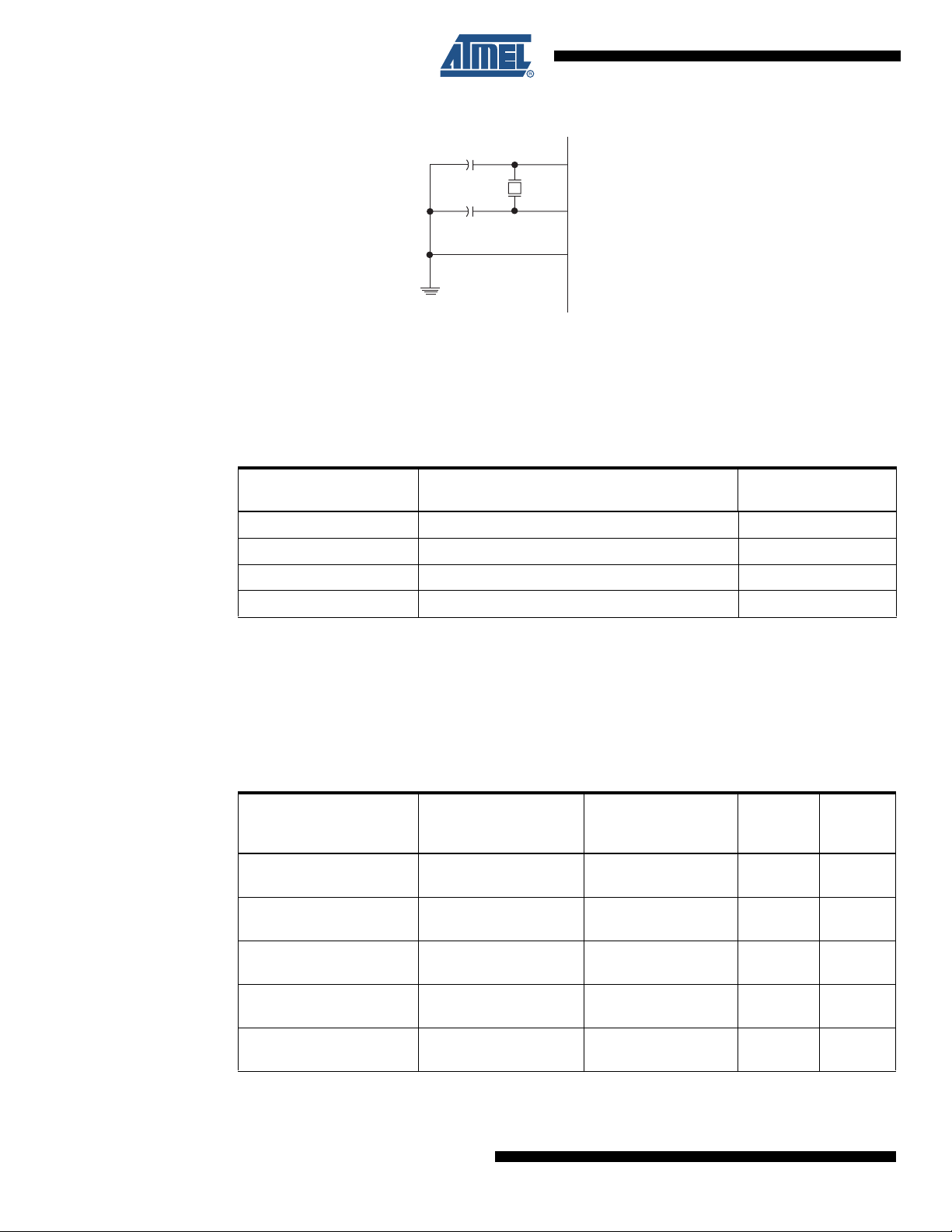
ATmega48P/88P/168P/328P
Figure 8-2. Crystal Oscillator Connections
2)
1)
C2
C1
XTAL2 (TOSC
XTAL1 (TOSC
GND
The Low Power Oscillator can operate in three different modes, each optimized for a specific frequency range. The operating mode is selected by the fuses CKSEL3..1 as shown in Table 8-3
on page 30.
Table 8-3. Low Power Crystal Oscillator Operating Modes
Frequency Range
(MHz)
0.4 - 0.9 – 100
0.9 - 3.0 12 - 22 101
3.0 - 8.0 12 - 22 110
8.0 - 16.0 12 - 22 111
(1)
Recommended Range for
Capacitors C1 and C2 (pF) CKSEL3..1
(3)
(2)
Notes: 1. The frequency ranges are preliminary values. Actual values are TBD.
2. This option should not be used with crystals, only with ceramic resonators.
3. If 8 MHz frequency exceeds the specification of the device (depends on VCC), the CKDIV8
Fuse can be programmed in order to divide the internal frequency by 8. It must be ensured
that the resulting divided clock meets the frequency specification of the device.
The CKSEL0 Fuse together with the SUT1..0 Fuses select the start-up times as shown in Table
8-4.
Table 8-4. Start-up Times for the Low Power Crystal Oscillator Clock Selection
Oscillator Source /
Power Conditions
Ceramic resonator, fast
rising power
Ceramic resonator, slowly
rising power
Ceramic resonator, BOD
enabled
Ceramic resonator, fast
rising power
Ceramic resonator, slowly
rising power
Start-up Time from
Power-down and
Power-save
258 CK 14CK + 4.1 ms
258 CK 14CK + 65 ms
1K CK 14CK
1K CK 14CK + 4.1 ms
1K CK 14CK + 65 ms
Additional Delay
from Reset
= 5.0V) CKSEL0 SUT1..0
(V
CC
(1)
(1)
(2)
(2)
(2)
000
001
010
011
100
30
8025D–AVR–03/08
Loading...