


 Loading...
BDTIC www.bdtic.com/ATMEL
Features
•High Performance, Low Power AVR® 8-Bit Microcontroller
•Advanced RISC Architecture
–120 Powerful Instructions – Most Single Clock Cycle Execution
–32 x 8 General Purpose Working Registers
–Fully Static Operation
•Non-Volatile Program and Data Memories
–2/4/8K Bytes of In-System Programmable Program Memory Flash
•Endurance: 10,000 Write/Erase Cycles
–128/256/512 Bytes of In-System Programmable EEPROM
•Endurance: 100,000 Write/Erase Cycles
–128/256/512 Bytes of Internal SRAM
–Data retention: 20 years at 85°C / 100 years at 25°C
–Programming Lock for Self-Programming Flash & EEPROM Data Security
•Peripheral Features
–One 8-Bit and One 16-Bit Timer/Counter with Two PWM Channels, Each
–10-bit ADC
•8 Single-Ended Channels
•12 Differential ADC Channel Pairs with Programmable Gain (1x / 20x)
–Programmable Watchdog Timer with Separate On-chip Oscillator
–On-Chip Analog Comparator
–Universal Serial Interface
•Special Microcontroller Features
–debugWIRE On-chip Debug System
–In-System Programmable via SPI Port
–Internal and External Interrupt Sources: Pin Change Interrupt on 12 Pins
–Low Power Idle, ADC Noise Reduction, Standby and Power-Down Modes
–Enhanced Power-on Reset Circuit
–Programmable Brown-Out Detection Circuit
–Internal Calibrated Oscillator
–On-Chip Temperature Sensor
•I/O and Packages
–Available in 20-Pin QFN/MLF & 14-Pin SOIC and PDIP
–Twelve Programmable I/O Lines
•Operating Voltage:
–1.8 – 5.5V for ATtiny24V/44V/84V
–2.7 – 5.5V for ATtiny24/44/84
•Speed Grade
–ATtiny24V/44V/84V
•0 – 4 MHz @ 1.8 – 5.5V
•0 – 10 MHz @ 2.7 – 5.5V
–ATtiny24/44/84
•0 – 10 MHz @ 2.7 – 5.5V
•0 – 20 MHz @ 4.5 – 5.5V
•Industrial Temperature Range: -40°C to +85°C
•Low Power Consumption
–Active Mode (1 MHz System Clock): 300 µA @ 1.8V
–Power-down Mode: 0.1 µA @ 1.8V
8-bit
Microcontroller with 2/4/8K Bytes In-System Programmable Flash
ATtiny24/44/84
Preliminary
Summary
Rev. 8006GS–AVR–01/08
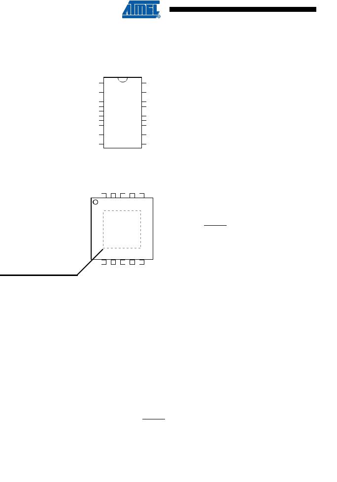
1. Pin Configurations
Figure 1-1. Pinout ATtiny24/44/84
PDIP/SOIC
|
|
VCC |
1 |
14 |
GND |
(PCINT8/XTAL1/CLKI) PB0 |
2 |
13 |
PA0 (ADC0/AREF/PCINT0) |
||
(PCINT9/XTAL2) PB1 |
3 |
12 |
PA1 (ADC1/AIN0/PCINT1) |
||
|
|
|
4 |
11 |
PA2 (ADC2/AIN1/PCINT2) |
(PCINT11/RESET/dW) |
PB3 |
||||
(PCINT10/INT0/OC0A/CKOUT) PB2 |
5 |
10 |
PA3 (ADC3/T0/PCINT3) |
||
(PCINT7/ICP/OC0B/ADC7) PA7 |
6 |
9 |
PA4 (ADC4/USCK/SCL/T1/PCINT4) |
||
(PCINT6/OC1A/SDA/MOSI/DI/ADC6) PA6 |
7 |
8 |
PA5 (ADC5/DO/MISO/OC1B/PCINT5) |
||
QFN/MLF
PA5 |
DNC |
DNC |
DNC |
PA6 |
Pin 16: PA6 (PCINT6/OC1A/SDA/MOSI/DI/ADC6)
Pin 20: PA5 (ADC5/DO/MISO/OC1B/PCINT5)
(ADC4/USCK/SCL/T1/PCINT4) PA4  1 (ADC3/T0/PCINT3) PA3
  2 (ADC2/AIN1/PCINT2) PA2
  3 (ADC1/AIN0/PCINT1) PA1
  4 (ADC0/AREF/PCINT0) PA0
  5
5
NOTE
Bottom pad should be soldered to ground. DNC: Do Not Connect
20 |
19 |
18 |
17 |
|
|
|
|
|
|
|
|
|
|
|
6 |
7 |
8 |
9 |
DNC |
DNC |
GND |
VCC |
16
DNC 10
15  PA7 (PCINT7/ICP/OC0B/ADC7)
14  PB2 (PCINT10/INT0/OC0A/CKOUT)
13  PB3 (PCINT11/RESET/dW)
12  PB1 (PCINT9/XTAL2)
11  PB0 (PCINT8/XTAL1/CLKI)
1.1Pin Descriptions
1.1.1VCC
Supply voltage.
1.1.2GND
Ground.
1.1.3Port B (PB3...PB0)
Port B is a 4-bit bi-directional I/O port with internal pull-up resistors (selected for each bit). The Port B output buffers have symmetrical drive characteristics with both high sink and source capability except PB3 which has the RESET capability. To use pin PB3 as an I/O pin, instead of RESET pin, program (‘0’) RSTDISBL fuse. As inputs, Port B pins that are externally pulled low will source current if the pull-up resistors are activated. The Port B pins are tri-stated when a reset condition becomes active, even if the clock is not running.
2 ATtiny24/44/84 
8006GS–AVR–01/08

 ATtiny24/44/84
Port B also serves the functions of various special features.
1.1.4RESET
Reset input. A low level on this pin for longer than the minimum pulse length will generate a reset, even if the clock is not running and provided the reset pin has not been disabled. Shorter pulses are not guaranteed to generate a reset.
The reset pin can also be used as a (weak) I/O pin.
1.1.5Port A (PA7...PA0)
Port A is a 8-bit bi-directional I/O port with internal pull-up resistors (selected for each bit). The Port A output buffers have symmetrical drive characteristics with both high sink and source capability. As inputs, Port A pins that are externally pulled low will source current if the pull-up resistors are activated. The Port A pins are tri-stated when a reset condition becomes active, even if the clock is not running.
Port A has alternate functions as analog inputs for the ADC, analog comparator, timer/counter, SPI and pin change interrupt.
3
8006GS–AVR–01/08

2. Overview
The ATtiny24/44/84 is a low-power CMOS 8-bit microcontroller based on the AVR enhanced RISC architecture. By executing powerful instructions in a single clock cycle, the ATtiny24/44/84 achieves throughputs approaching 1 MIPS per MHz allowing the system designer to optimize power consumption versus processing speed.
Figure 2-1. |
Block Diagram |
|
|
|
VCC |
|
|
|
|
|
|
|
8-BIT DATABUS |
INTERNAL |
|
|
|
|
|
|
|
|
INTERNAL |
CALIBRATED |
|
|
|
OSCILLATOR |
OSCILLATOR |
GND |
|
|
|
|
|
PROGRAM |
STACK |
WATCHDOG |
TIMING AND |
|
COUNTER |
POINTER |
TIMER |
CONTROL |
|
PROGRAM |
|
MCU CONTROL |
|
|
SRAM |
REGISTER |
|
|
|
FLASH |
|
||
|
|
|
|
|
|
|
|
MCU STATUS |
|
|
INSTRUCTION |
GENERAL |
REGISTER |
|
|
REGISTER |
PURPOSE |
|
|
|
|
REGISTERS |
|
|
|
|
|
TIMER/ |
|
|
INSTRUCTION |
X |
COUNTER0 |
|
|
Y |
|
|
|
|
DECODER |
Z |
|
|
|
|
|
TIMER/ |
|
|
|
|
COUNTER1 |
|
|
CONTROL |
ALU |
|
|
|
LINES |
|
|
|
|
|
|
|
|
|
|
STATUS |
|
|
|
|
REGISTER |
|
|
|
|
|
INTERRUPT |
|
|
|
|
UNIT |
|
|
PROGRAMMING |
ISP INTERFACE |
EEPROM |
OSCILLATORS |
|
LOGIC |
|||
|
|
|
|
+ - |
ANALOG COMPARATOR |
DATA REGISTER |
|
DATA DIR. |
|
|
ADC |
|
DATA REGISTER |
|
DATA DIR. |
|
||||||||||||||||||||||||||||
|
|
|
PORT A |
REG.PORT A |
|
|
|
|
|
PORT B |
|
REG.PORT B |
|
|||||||||||||||||||||||||
|
|
|
|
|
|
|
|
|
|
|
|
|
|
|
|
|
|
|
|
|
|
|
|
|
|
|
|
|
|
|
|
|
|
|
|
|
|
|
|
|
|
|
|
|
|
|
|
|
|
|
|
|
|
|
|
|
|
|
|
|
|
|
|
|
|
|
|
|
|
|
|
|
|
|
|
|
|
|
|
|
|
|
|
|
|
|
|
|
|
|
|
|
|
|
|
|
|
|
|
|
|
|
|
|
|
|
|
|
|
|
||||||
|
|
|
|
|
|
|
|
PORT A DRIVERS |
|
|
|
|
|
|
|
|
PORT B DRIVERS |
|
||||||||||||||||||||
|
|
|
|
|
|
|
|
|
|
|
|
|
|
|
|
|
|
|
|
|
|
|
|
|
|
|
|
|
|
|
|
|
|
|
|
|
|
|
|
|
|
|
|
|
|
|
|
|
|
|
|
|
|
|
|
|
|
|
|
|
|
|
|
|
|
|
|
|
|
|
|
|
|
|
|
|
|
|
|
|
|
|
|
|
|
|
|
|
|
|
|
|
|
|
|
|
|
|
|
|
|
|
|
|
|
|
|
|
|
|
|
|
|
|
|
|
PA7-PA0 |
PB3-PB0 |
The AVR core combines a rich instruction set with 32 general purpose working registers. All 32 registers are directly connected to the Arithmetic Logic Unit (ALU), allowing two independent registers to be accessed in one single instruction executed in one clock cycle. The resulting architecture is more code efficient while achieving throughputs up to ten times faster than conventional CISC microcontrollers.
4 ATtiny24/44/84
8006GS–AVR–01/08

 ATtiny24/44/84
The ATtiny24/44/84 provides the following features: 2/4/8K byte of In-System Programmable Flash, 128/256/512 bytes EEPROM, 128/256/512 bytes SRAM, 12 general purpose I/O lines, 32 general purpose working registers, a 8-bit Timer/Counter with two PWM channels, a 16-bit timer/counter with two PWM channels, Internal and External Interrupts, a 8-channel 10-bit ADC, programmable gain stage (1x, 20x) for 12 differential ADC channel pairs, a programmable Watchdog Timer with internal Oscillator, internal calibrated oscillator, and four software selectable power saving modes. Idle mode stops the CPU while allowing the SRAM, Timer/Counter, ADC, Analog Comparator, and Interrupt system to continue functioning. ADC Noise Reduction mode minimizes switching noise during ADC conversions by stopping the CPU and all I/O modules except the ADC. In Power-down mode registers keep their contents and all chip functions are disbaled until the next interrupt or hardware reset. In Standby mode, the crystal/resonator oscillator is running while the rest of the device is sleeping, allowing very fast start-up combined with low power consumption.
The device is manufactured using Atmel’s high density non-volatile memory technology. The onchip ISP Flash allows the Program memory to be re-programmed in-system through an SPI serial interface, by a conventional non-volatile memory programmer or by an on-chip boot code running on the AVR core.
The ATtiny24/44/84 AVR is supported with a full suite of program and system development tools including: C Compilers, Macro Assemblers, Program Debugger/Simulators and Evaluation kits.
5
8006GS–AVR–01/08

3. About
3.1Resources
A comprehensive set of drivers, application notes, data sheets and descriptions on development tools are available for download at http://www.atmel.com/avr.
3.2Code Examples
This documentation contains simple code examples that briefly show how to use various parts of the device. These code examples assume that the part specific header file is included before compilation. Be aware that not all C compiler vendors include bit definitions in the header files and interrupt handling in C is compiler dependent. Please confirm with the C compiler documentation for more details.
For I/O Registers located in the extended I/O map, “IN”, “OUT”, “SBIS”, “SBIC”, “CBI”, and “SBI” instructions must be replaced with instructions that allow access to extended I/O. Typically, this means “LDS” and “STS” combined with “SBRS”, “SBRC”, “SBR”, and “CBR”. Note that not all AVR devices include an extended I/O map.
3.3Data Retention
Reliability Qualification results show that the projected data retention failure rate is much less than 1 PPM over 20 years at 85°C or 100 years at 25°C.
3.4Disclaimer
Typical values contained in this datasheet are based on simulations and characterization of other AVR microcontrollers manufactured on the same process technology. Min and Max values will be available after the device is characterized.
6 ATtiny24/44/84 
8006GS–AVR–01/08

 ATtiny24/44/84
4. |
Register Summary |
|
|
|
|
|
|
|
|
|||
|
|
|
|
|
|
|
|
|
|
|
|
|
|
Address |
Name |
Bit 7 |
Bit 6 |
Bit 5 |
Bit 4 |
Bit 3 |
Bit 2 |
Bit 1 |
Bit 0 |
Page |
|
|
|
|
|
|
|
|
|
|
|
|
|
|
|
0x3F (0x5F) |
SREG |
I |
T |
H |
S |
V |
N |
Z |
C |
|
|
|
0x3E (0x5E) |
SPH |
– |
– |
– |
– |
– |
– |
SP9 |
SP8 |
|
|
|
0x3D (0x5D) |
SPL |
SP7 |
SP6 |
SP5 |
SP4 |
SP3 |
SP2 |
SP1 |
SP0 |
|
|
|
0x3C (0x5C) |
OCR0B |
|
|
Timer/Counter0 – Output Compare Register B |
|
|
|
||||
|
0x3B (0x5B) |
GIMSK |
– |
INT0 |
PCIE1 |
PCIE0 |
– |
– |
– |
– |
|
|
|
0x3A (0x5A |
GIFR |
– |
INTF0 |
PCIF1 |
PCIF0 |
– |
– |
– |
– |
|
|
|
0x39 |
(0x59) |
TIMSK0 |
– |
– |
– |
– |
– |
OCIE0B |
OCIE0A |
TOIE0 |
|
|
0x38 |
(0x58) |
TIFR0 |
|
– |
– |
– |
– |
OCF0B |
OCF0A |
TOV0 |
|
|
0x37 |
(0x57) |
SPMCSR |
– |
– |
– |
CTPB |
RFLB |
PGWRT |
PGERS |
SPMEN |
|
|
0x36 |
(0x56) |
OCR0A |
|
|
Timer/Counter0 – Output Compare Register A |
|
|
|
|||
|
0x35 |
(0x55) |
MCUCR |
BODS |
PUD |
SE |
SM1 |
SM0 |
BODSE |
ISC01 |
ISC00 |
|
|
0x34 |
(0x54) |
MCUSR |
– |
– |
– |
– |
WDRF |
BORF |
EXTRF |
PORF |
|
|
0x33 |
(0x53) |
TCCR0B |
FOC0A |
FOC0B |
– |
– |
WGM02 |
CS02 |
CS01 |
CS00 |
|
|
0x32 |
(0x52) |
TCNT0 |
|
|
|
Timer/Counter0 |
|
|
|
|
|
|
0x31 |
(0x51) |
OSCCAL |
CAL7 |
CAL6 |
CAL5 |
CAL4 |
CAL3 |
CAL2 |
CAL1 |
CAL0 |
|
|
0x30 |
(0x50) |
TCCR0A |
COM0A1 |
COM0A0 |
COM0B1 |
COM0B0 |
– |
|
WGM01 |
WGM00 |
|
|
0x2F |
(0x4F) |
TCCR1A |
COM1A1 |
COM1A0 |
COM1B1 |
COM1B0 |
– |
|
WGM11 |
WGM10 |
|
|
0x2E |
(0x4E) |
TCCR1B |
ICNC1 |
ICES1 |
– |
WGM13 |
WGM12 |
CS12 |
CS11 |
CS10 |
|
|
0x2D |
(0x4D) |
TCNT1H |
|
|
Timer/Counter1 – Counter Register High Byte |
|
|
|
|||
|
0x2C |
(0x4C) |
TCNT1L |
|
|
Timer/Counter1 – Counter Register Low Byte |
|
|
|
|||
|
0x2B |
(0x4B) |
OCR1AH |
|
|
Timer/Counter1 – Compare Register A High Byte |
|
|
|
|||
|
0x2A |
(0x4A) |
OCR1AL |
|
|
Timer/Counter1 – Compare Register A Low Byte |
|
|
|
|||
|
0x29 |
(0x49) |
OCR1BH |
|
|
Timer/Counter1 – Compare Register B High Byte |
|
|
|
|||
|
0x28 |
(0x48) |
OCR1BL |
|
|
Timer/Counter1 – Compare Register B Low Byte |
|
|
|
|||
|
0x27 |
(0x47) |
DWDR |
|
|
|
DWDR[7:0] |
|
|
|
|
|
|
0x26 |
(0x46) |
CLKPR |
CLKPCE |
– |
– |
– |
CLKPS3 |
CLKPS2 |
CLKPS1 |
CLKPS0 |
|
|
0x25 |
(0x45) |
ICR1H |
|
|
Timer/Counter1 - Input Capture Register High Byte |
|
|
|
|||
|
0x24 |
(0x44) |
ICR1L |
|
|
Timer/Counter1 - Input Capture Register Low Byte |
|
|
|
|||
|
0x23 |
(0x43) |
GTCCR |
TSM |
– |
– |
– |
– |
– |
– |
PSR10 |
|
|
0x22 |
(0x42) |
TCCR1C |
FOC1A |
FOC1B |
– |
– |
– |
– |
– |
– |
|
|
0x21 |
(0x41) |
WDTCSR |
WDIF |
WDIE |
WDP3 |
WDCE |
WDE |
WDP2 |
WDP1 |
WDP0 |
|
|
0x20 |
(0x40) |
PCMSK1 |
– |
– |
– |
– |
PCINT11 |
PCINT10 |
PCINT9 |
PCINT8 |
|
|
0x1F (0x3F) |
EEARH |
– |
– |
– |
– |
– |
– |
– |
EEAR8 |
|
|
|
0x1E (0x3E) |
EEARL |
EEAR7 |
EEAR6 |
EEAR5 |
EEAR4 |
EEAR3 |
EEAR2 |
EEAR1 |
EEAR0 |
|
|
|
0x1D (0x3D) |
EEDR |
|
|
|
EEPROM Data Register |
|
|
|
|
||
|
0x1C (0x3C) |
EECR |
– |
– |
EEPM1 |
EEPM0 |
EERIE |
EEMPE |
EEPE |
EERE |
|
|
|
0x1B (0x3B) |
PORTA |
PORTA7 |
PORTA6 |
PORTA5 |
PORTA4 |
PORTA3 |
PORTA2 |
PORTA1 |
PORTA0 |
|
|
|
0x1A (0x3A) |
DDRA |
DDA7 |
DDA6 |
DDA5 |
DDA4 |
DDA3 |
DDA2 |
DDA1 |
DDA0 |
|
|
|
0x19 |
(0x39) |
PINA |
PINA7 |
PINA6 |
PINA5 |
PINA4 |
PINA3 |
PINA2 |
PINA1 |
PINA0 |
|
|
0x18 |
(0x38) |
PORTB |
– |
– |
– |
– |
PORTB3 |
PORTB2 |
PORTB1 |
PORTB0 |
|
|
0x17 |
(0x37) |
DDRB |
– |
– |
– |
– |
DDB3 |
DDB2 |
DDB1 |
DDB0 |
|
|
0x16 |
(0x36) |
PINB |
– |
– |
– |
– |
PINB3 |
PINB2 |
PINB1 |
PINB0 |
|
|
0x15 |
(0x35) |
GPIOR2 |
|
|
|
General Purpose I/O Register 2 |
|
|
|
|
|
|
0x14 |
(0x34) |
GPIOR1 |
|
|
|
General Purpose I/O Register 1 |
|
|
|
|
|
|
0x13 |
(0x33) |
GPIOR0 |
|
|
|
General Purpose I/O Register 0 |
|
|
|
|
|
|
0x12 |
(0x32) |
PCMSK0 |
PCINT7 |
PCINT6 |
PCINT5 |
PCINT4 |
PCINT3 |
PCINT2 |
PCINT1 |
PCINT0 |
|
|
0x11 (0x31)) |
Reserved |
|
|
|
|
– |
|
|
|
|
|
|
0x10 |
(0x30) |
USIBR |
|
|
|
USI Buffer Register |
|
|
|
|
|
|
0x0F |
(0x2F) |
USIDR |
|
|
|
USI Data Register |
|
|
|
|
|
|
0x0E |
(0x2E) |
USISR |
USISIF |
USIOIF |
USIPF |
USIDC |
USICNT3 |
USICNT2 |
USICNT1 |
USICNT0 |
|
|
0x0D (0x2D) |
USICR |
USISIE |
USIOIE |
USIWM1 |
USIWM0 |
USICS1 |
USICS0 |
USICLK |
USITC |
|
|
|
0x0C (0x2C) |
TIMSK1 |
– |
– |
ICIE1 |
– |
– |
OCIE1B |
OCIE1A |
TOIE1 |
|
|
|
0x0B (0x2B) |
TIFR1 |
– |
– |
ICF1 |
– |
– |
OCF1B |
OCF1A |
TOV1 |
|
|
|
0x0A (0x2A) |
Reserved |
|
|
|
|
– |
|
|
|
|
|
|
0x09 |
(0x29) |
Reserved |
|
|
|
|
– |
|
|
|
|
|
0x08 |
(0x28) |
ACSR |
ACD |
ACBG |
ACO |
ACI |
ACIE |
ACIC |
ACIS1 |
ACIS0 |
|
|
0x07 |
(0x27) |
ADMUX |
REFS1 |
REFS0 |
MUX5 |
MUX4 |
MUX3 |
MUX2 |
MUX1 |
MUX0 |
|
|
0x06 |
(0x26) |
ADCSRA |
ADEN |
ADSC |
ADATE |
ADIF |
ADIE |
ADPS2 |
ADPS1 |
ADPS0 |
|
|
0x05 |
(0x25) |
ADCH |
|
|
|
ADC Data Register High Byte |
|
|
|
|
|
|
0x04 |
(0x24) |
ADCL |
|
|
|
ADC Data Register Low Byte |
|
|
|
|
|
|
0x03 |
(0x23) |
ADCSRB |
BIN |
ACME |
– |
ADLAR |
– |
ADTS2 |
ADTS1 |
ADTS0 |
|
|
0x02 |
(0x22) |
Reserved |
|
|
|
|
– |
|
|
|
|
|
0x01 |
(0x21) |
DIDR0 |
ADC7D |
ADC6D |
ADC5D |
ADC4D |
ADC3D |
ADC2D |
ADC1D |
ADC0D |
|
|
0x00 |
(0x20) |
PRR |
– |
– |
– |
– |
PRTIM1 |
PRTIM0 |
PRUSI |
PRADC |
|
|
|
|
|
|
|
|
|
|
|
|
|
|
7
8006GS–AVR–01/08

Note:
8
1.For compatibility with future devices, reserved bits should be written to zero if accessed. Reserved I/O memory addresses should never be written.
2.I/O Registers within the address range 0x00 - 0x1F are directly bit-accessible using the SBI and CBI instructions. In these registers, the value of single bits can be checked by using the SBIS and SBIC instructions.
3.Some of the Status Flags are cleared by writing a logical one to them. Note that, unlike most other AVRs, the CBI and SBI instructions will only operation the specified bit, and can therefore be used on registers containing such Status Flags. The CBI and SBI instructions work with registers 0x00 to 0x1F only.
ATtiny24/44/84 
8006GS–AVR–01/08
Loading...