


 Loading...
BDTIC www.bdtic.com/ATMEL
Features
•Compatible with MCS®-51 Products
•12K Bytes of In-System Programmable (ISP) Flash Program Memory
–SPI Serial Interface for Program Downloading
–Endurance: 10,000 Write/Erase Cycles
•2K Bytes EEPROM Data Memory
–Endurance: 100,000 Write/Erase Cycles
•64-byte User Signature Array
•2.7V to 5.5V Operating Range
•Fully Static Operation: 0 Hz to 24 MHz (in x1 and x2 Modes)
•Three-level Program Memory Lock
•256 x 8-bit Internal RAM
•32 Programmable I/O Lines
•Three 16-bit Timer/Counters
•Nine Interrupt Sources
•Enhanced UART Serial Port with Framing Error Detection and Automatic Address Recognition
•Enhanced SPI (Double Write/Read Buffered) Serial Interface
•Low-power Idle and Power-down Modes
•Interrupt Recovery from Power-down Mode
•Programmable Watchdog Timer
•Dual Data Pointer
•Power-off Flag
•Flexible ISP Programming (Byte and Page Modes)
–Page Mode: 64 Bytes/Page for Code Memory, 32 Bytes/Page for Data Memory
•Four-level Enhanced Interrupt Controller
•Programmable and Fuseable x2 Clock Option
•Internal Power-on Reset
•42-pin PDIP Package Option for Reduced EMC Emission
•Green (Pb/Halide-free) Packaging Option
1. Description
The AT89S8253 is a low-power, high-performance CMOS 8-bit microcontroller with 12K bytes of In-System Programmable (ISP) Flash program memory and 2K bytes of EEPROM data memory. The device is manufactured using Atmel’s high-density nonvolatile memory technology and is compatible with the industry-standard MCS-51 instruction set and pinout. The on-chip downloadable Flash allows the program memory to be reprogrammed in-system through an SPI serial interface or by a conventional nonvolatile memory programmer. By combining a versatile 8-bit CPU with downloadable Flash on a monolithic chip, the Atmel AT89S8253 is a powerful microcontroller which provides a highly-flexible and cost-effective solution to many embedded control applications.
8-bit Microcontroller with 12K Bytes Flash and 2K Bytes EEPROM
AT89S8253
3286K–MICRO–12/06

The AT89S8253 provides the following standard features: 12K bytes of In-System Programmable Flash, 2K bytes of EEPROM, 256 bytes of RAM, 32 I/O lines, programmable watchdog timer, two data pointers, three 16-bit timer/counters, a six-vector, four-level interrupt architecture, a full duplex serial port, on-chip oscillator, and clock circuitry. In addition, the AT89S8253 is designed with static logic for operation down to zero frequency and supports two software selectable power saving modes. The Idle Mode stops the CPU while allowing the RAM, timer/counters, serial port, and interrupt system to continue functioning. The Power-down mode saves the RAM contents but freezes the oscillator, disabling all other chip functions until the next external interrupt or hardware reset.
The on-board Flash/EEPROM is accessible through the SPI serial interface. Holding RESET active forces the SPI bus into a serial programming interface and allows the program memory to be written to or read from, unless one or more lock bits have been activated.
2. Pin Configurations
2.140P6 – 40-lead PDIP
(T2) |
P1.0 |
|
1 |
40 |
|
VCC |
|
|
||
|
|
|
|
|||||||
(T2 EX) P1.1 |
|
2 |
39 |
|
P0.0 |
(AD0) |
||||
|
|
|||||||||
|
|
|
P1.2 |
|
3 |
38 |
|
P0.1 |
(AD1) |
|
|
|
|
|
|
||||||
|
|
|
P1.3 |
|
4 |
37 |
|
P0.2 |
(AD2) |
|
|
|
|
|
|
||||||
|
|
P1.4 |
|
5 |
36 |
|
P0.3 |
(AD3) |
||
(SS) |
|
|
||||||||
|
|
|||||||||
(MOSI) P1.5 |
|
6 |
35 |
|
P0.4 |
(AD4) |
||||
|
|
|||||||||
(MISO) P1.6 |
|
7 |
34 |
|
P0.5 |
(AD5) |
||||
|
|
|||||||||
(SCK) P1.7 |
|
8 |
33 |
|
P0.6 |
(AD6) |
||||
|
|
|||||||||
|
|
|
RST |
|
9 |
32 |
|
P0.7 |
(AD7) |
|
|
|
|
|
|
||||||
(RXD) P3.0 |
|
10 |
31 |
|
EA/VPP |
|||||
|
|
|||||||||
(TXD) P3.1 |
|
11 |
30 |
|
ALE/P |
|
|
|||
|
|
ROG |
||||||||
|
|
|||||||||
(INT0) P3.2 |
|
12 |
29 |
|
PSEN |
|||||
|
|
|||||||||
(INT1) P3.3 |
|
13 |
28 |
|
P2.7 |
(A15) |
||||
|
|
|||||||||
(T0) P3.4 |
|
14 |
27 |
|
P2.6 |
(A14) |
||||
|
|
|||||||||
(T1) P3.5 |
|
15 |
26 |
|
P2.5 |
(A13) |
||||
|
||||||||||
(WR) P3.6 |
|
16 |
25 |
|
P2.4 |
(A12) |
||||
(RD) P3.7 |
|
17 |
24 |
|
P2.3 |
(A11) |
||||
|
XTAL2 |
|
18 |
23 |
|
P2.2 |
(A10) |
|||
|
XTAL1 |
|
19 |
22 |
|
P2.1 |
(A9) |
|||
|
|
|
GND |
|
20 |
21 |
|
P2.0 |
(A8) |
|
|
|
|
|
|
|
|
|
|
|
|
2.244A – 44-lead TQFP
|
(SS) |
|
|
(T2 EX) |
(T2) |
|
VCC |
(AD0) |
(AD1) |
(AD2) |
(AD3) |
|
|
|
|
||||||||
|
|
|
|
||||||||
|
P1.4 |
P1.3 |
P1.2 |
P1.1 |
P1.0 |
NC |
P0.0 |
P0.1 |
P0.2 |
P0.3 |
|
44 |
43 |
42 |
41 |
40 |
39 |
38 |
37 |
36 |
35 |
34 |
|
(MOSI) P1.5 |
1 |
|
33 |
P0.4 |
(AD4) |
||
(MISO) P1.6 |
2 |
|
32 |
P0.5 |
(AD5) |
||
(SCK) P1.7 |
3 |
|
31 |
P0.6 |
(AD6) |
||
RST |
4 |
|
30 |
P0.7 |
(AD7) |
||
(RXD) P3.0 |
5 |
|
29 |
EA/VPP |
|||
NC |
6 |
|
28 |
NC |
|
|
|
(TXD) P3.1 |
7 |
|
27 |
ALE/P |
ROG |
|
|
(INT0) P3.2 |
8 |
|
26 |
PSEN |
|||
(INT1) P3.3 |
9 |
|
25 |
P2.7 |
(A15) |
||
(T0) P3.4 |
10 |
|
24 |
P2.6 |
(A14) |
||
(T1) P3.5 |
11 |
|
23 |
P2.5 |
(A13) |
||
|
12 13 14 15 16 17 18 19 20 21 22 |
|
|
|
|||
|
|
(WR) P3.6 |
|
(RD) P3.7 XTAL2 XTAL1 GND GND (A8) P2.0 (A9) P2.1 (A10) P2.2 (A11) P2.3 (A12) P2.4 |
|
|
|
|
|
|
|
|
|
||
|
|
|
|
|
|
||
2 AT89S8253
3286K–MICRO–12/06

AT89S8253
2.344J – 44-lead PLCC
|
|
P1.4 (SS) |
|
|
|
|
|
|
|
|
|
(MOSI) P1.5 |
6 |
|
|
7 |
|
||
(MISO) P1.6 |
8 |
|
|
(SCK) P1.7 |
9 |
|
|
RST |
10 |
|
|
(RXD) P3.0 |
11 |
|
|
NC |
12 |
|
|
(TXD) P3.1 |
13 |
|
|
(INT0) P3.2 |
14 |
|
|
(INT1) P3.3 |
15 |
|
|
(T0) P3.4 |
16 |
|
|
17 |
|
||
(T1) P3.5 |
|
||
18 |
|
||
|
|
||
|
|
(WR) P3.6 |
|
|
|
|
|
|
|
||
|
|
|
|
5 P1.3
(RD) P3.7 19
4 P1.2
XTAL2 20
3 P1.1 (T2 EX)
XTAL1 21
2 P1.0 (T2)
GND 22
1 NC
NC 23
44 VCC
(A8) P2.0 24
43 P0.0 (AD0)
(A9) P2.1 25
42 P0.1 (AD1)
(A10) P2.2 26
41 P0.2 (AD2)
(A11) P2.3 27
P0.3 (AD3) |
|
|
|
40 |
P0.4 |
(AD4) |
|
39 |
|||
38 |
P0.5 |
(AD5) |
|
37 |
P0.6 |
(AD6) |
|
36 |
P0.7 |
(AD7) |
|
35 |
EA/VPP |
||
34 |
NC |
|
|
33 |
ALE/P |
ROG |
|
32 |
PSEN |
||
31 |
P2.7 |
(A15) |
|
30 |
P2.6 |
(A14) |
|
29 |
P2.5 |
(A13) |
|
28 |
|
|
|
(A12) P2.4 |
|
|
|
2.442PS6 – PDIP
|
|
|
|
|
|
RST |
|
1 |
42 |
|
|
P1.7 |
(SCK) |
|||||
|
|
|
|
|
|
|
|
|
||||||||||
(RXD) P3.0 |
|
2 |
41 |
|
|
P1.6 |
(MISO) |
|||||||||||
(TXD) P3.1 |
|
3 |
40 |
|
|
P1.5 |
(MOSI) |
|||||||||||
|
|
|||||||||||||||||
|
|
|
P3.2 |
|
4 |
39 |
|
|
P1.4 |
|
|
|
|
|
||||
|
(INT0) |
|
|
(SS) |
||||||||||||||
|
|
|
|
P3.3 |
|
5 |
38 |
|
|
P1.3 |
|
|
|
|
|
|||
(INT1) |
|
|
|
|
|
|
|
|||||||||||
|
|
(T0) |
P3.4 |
|
6 |
37 |
|
|
P1.2 |
|
|
|
|
|
||||
|
|
|
|
|
|
|
||||||||||||
|
|
(T1) |
P3.5 |
|
7 |
36 |
|
|
P1.1 |
(T2EX) |
||||||||
|
|
|||||||||||||||||
|
|
|
|
|
P3.6 |
|
8 |
35 |
|
|
P1.0 |
(T2) |
||||||
(WR) |
|
|
||||||||||||||||
|
|
|
P3.7 |
|
9 |
34 |
|
|
VDD |
|
|
|
|
|
||||
|
(RD) |
|
|
|
|
|
|
|
||||||||||
|
|
|
XTAL2 |
|
10 |
33 |
|
|
PWRVDD |
|||||||||
|
|
|||||||||||||||||
|
|
|
XTAL1 |
|
11 |
32 |
|
|
P0.0 |
(AD0) |
||||||||
|
|
|||||||||||||||||
|
|
|
|
|
|
GND |
|
12 |
31 |
|
|
P0.1 |
(AD1) |
|||||
|
|
|
|
|
|
|
|
|||||||||||
|
PWRGND |
|
13 |
30 |
|
|
P0.2 |
(AD2) |
||||||||||
|
|
|||||||||||||||||
|
|
(A8) |
P2.0 |
|
14 |
29 |
|
|
P0.3 |
(AD3) |
||||||||
|
|
|||||||||||||||||
|
|
(A9) |
P2.1 |
|
15 |
28 |
|
|
P0.4 |
(AD4) |
||||||||
|
||||||||||||||||||
(A10) |
P2.2 |
|
16 |
27 |
|
|
P0.5 |
(AD5) |
||||||||||
(A11) |
P2.3 |
|
17 |
26 |
|
|
P0.6 |
(AD6) |
||||||||||
(A12) |
P2.4 |
|
18 |
25 |
|
|
P0.7 |
(AD7) |
||||||||||
(A13) |
P2.5 |
|
19 |
24 |
|
|
|
|
|
|
||||||||
|
|
|
EA/VPP |
|||||||||||||||
(A14) P2.6 |
|
20 |
23 |
|
|
|
|
|
|
|||||||||
|
|
|
ALE/PROG |
|||||||||||||||
(A15) P2.7 |
|
21 |
22 |
|
|
|
|
|||||||||||
|
|
|
PSEN |
|||||||||||||||
|
|
|
|
|
|
|
|
|
|
|
|
|
|
|
|
|
|
|
3. Pin Description
3.1VCC
Supply voltage (all packages except 42-PDIP).
3.2GND
Ground (all packages except 42-PDIP; for 42-PDIP GND connects only the logic core and the embedded program/data memories).
3.3VDD
Supply voltage for the 42-PDIP which connects only the logic core and the embedded program/data memories.
3.4PWRVDD
Supply voltage for the 42-PDIP which connects only the I/O Pad Drivers.
The application board must connect both VDD and PWRVDD to the board supply voltage.
3
3286K–MICRO–12/06

3.5PWRGND
Ground for the 42-PDIP which connects only the I/O Pad Drivers. PWRGND and GND are weakly connected through the common silicon substrate, but not through any metal links. The application board must connect both GND and PWRGND to the board ground.
3.6Port 0
Port 0 is an 8-bit open drain bi-directional I/O port. As an output port, each pin can sink six TTL inputs. When 1s are written to port 0 pins, the pins can be used as high-impedance inputs.
Port 0 can also be configured to be the multiplexed low-order address/data bus during accesses to external program and data memory. In this mode, P0 has internal pull-ups.
Port 0 also receives the code bytes during Flash programming and outputs the code bytes during program verification. External pull-ups are required during program verification.
3.7Port 1
Port 1 is an 8-bit bi-directional I/O port with internal pull-ups. The Port 1 output buffers can sink/source six TTL inputs. When 1s are written to Port 1 pins, they are pulled high by the weak internal pull-ups and can be used as inputs. As inputs, Port 1 pins that are externally being pulled low will source current (IIL,150 µA typical) because of the weak internal pull-ups.
Some Port 1 pins provide additional functions. P1.0 and P1.1 can be configured to be the timer/counter 2 external count input (P1.0/T2) and the timer/counter 2 trigger input (P1.1/T2EX), respectively.
Furthermore, P1.4, P1.5, P1.6, and P1.7 can be configured as the SPI slave port select, data input/output and shift clock input/output pins as shown in the following table.
Port Pin |
Alternate Functions |
||
|
|
||
P1.0 |
T2 (external count input to Timer/Counter 2), clock-out |
||
|
|
||
P1.1 |
T2EX (Timer/Counter 2 capture/reload trigger and direction control) |
||
|
|
|
|
P1.4 |
|
|
(Slave port select input) |
|
SS |
||
|
|
||
P1.5 |
MOSI (Master data output, slave data input pin for SPI channel) |
||
|
|
||
P1.6 |
MISO (Master data input, slave data output pin for SPI channel) |
||
|
|
||
P1.7 |
SCK (Master clock output, slave clock input pin for SPI channel) |
||
|
|
|
|
Port 1 also receives the low-order address bytes during Flash programming and verification.
3.8Port 2
Port 2 is an 8-bit bi-directional I/O port with internal pull-ups. The Port 2 output buffers can sink/source six TTL inputs. When 1s are written to Port 2 pins, they are pulled high by the weak internal pull-ups and can be used as inputs. As inputs, Port 2 pins that are externally being pulled low will source current (IIL,150 µA typical) because of the weak internal pull-ups.
Port 2 emits the high-order address byte during fetches from external program memory and during accesses to external data memory that use 16-bit addresses (MOVX @ DPTR). In this application, Port 2 uses strong internal pull-ups when emitting 1s. During accesses to external data memory that use 8-bit addresses (MOVX @ RI), Port 2 emits the contents of the P2 Special Function Register.
Port 2 also receives the high-order address bits and some control signals during Flash programming and verification.
4 AT89S8253 
3286K–MICRO–12/06

AT89S8253
3.9Port 3
Port 3 is an 8-bit bi-directional I/O port with internal pull-ups. The Port 3 output buffers can sink/source six TTL inputs. When 1s are written to Port 3 pins, they are pulled high by the weak internal pull-ups and can be used as inputs. As inputs, Port 3 pins that are externally being pulled low will source current (IIL,150 µA typical) because of the weak internal pull-ups.
Port 3 receives some control signals for Flash programming and verification.
Port 3 also serves the functions of various special features of the AT89S8253, as shown in the following table.
Port Pin |
|
Alternate Functions |
|||||||||
|
|
|
|||||||||
P3.0 |
|
RXD (serial input port) |
|||||||||
|
|
|
|||||||||
P3.1 |
|
TXD (serial output port) |
|||||||||
|
|
|
|
|
|
|
|
||||
P3.2 |
|
|
|
|
|
|
(external interrupt 0)(1) |
||||
|
|
INT0 |
|||||||||
P3.3 |
|
|
|
|
|
|
(external interrupt 1)(1) |
||||
|
|
INT1 |
|||||||||
P3.4 |
|
T0 (timer 0 external input) |
|||||||||
|
|
|
|||||||||
P3.5 |
|
T1 (timer 1 external input) |
|||||||||
|
|
|
|
|
|
||||||
P3.6 |
|
|
|
|
(external data memory write strobe) |
||||||
|
|
WR |
|||||||||
P3.7 |
|
|
|
(external data memory read strobe) |
|||||||
|
|
RD |
|||||||||
Note: 1. |
All pins in ports 1 and 2 and almost all pins in port 3 (the exceptions are P3.2 |
INT0 |
and P3.3 |
||||||||
|
INT1) |
|
have their inputs disabled in the Power-down mode. Port pins P3.2 |
(INT0) |
and P3.3 |
||||||
(INT1) are active even in Power-down mode (to be able to sense an interrupt request to exit the Power-down mode) and as such still have their weak internal pull-ups turned on.
3.10RST
Reset input. A high on this pin for at least two machine cycles while the oscillator is running resets the device.
3.11ALE/PROG
Address Latch Enable. ALE/PROG is an output pulse for latching the low byte of the address (on its falling edge) during accesses to external memory. This pin is also the program pulse input (PROG) during Flash programming.
In normal operation, ALE is emitted at a constant rate of 1/6 the oscillator frequency and may be used for external timing or clocking purposes. Note, however, that one ALE pulse is skipped during each access to external data memory.
If desired, ALE operation can be disabled by setting bit 0 of the AUXR SFR at location 8EH. With the bit set, ALE is active only during a MOVX or MOVC instruction. Otherwise, the pin is weakly pulled high. Setting the ALE-disable bit has no effect if the microcontroller is in external execution mode.
3.12PSEN
Program Store Enable. PSEN is the read strobe to external program memory (active low).
When the AT89S8253 is executing code from external program memory, PSEN is activated twice each machine cycle, except that two PSEN activations are skipped during each access to external data memory.
5
3286K–MICRO–12/06
3.13EA/VPP
External Access Enable. EA must be strapped to GND in order to enable the device to fetch code from external program memory locations starting at 0000H up to FFFFH. Note, however, that if lock bit 1 is programmed, EA will be internally latched on reset.
EA should be strapped to VCC for internal program executions. This pin also receives the 12-volt programming enable voltage (VPP) during Flash programming when 12-volt programming is selected.
3.14XTAL1
Input to the inverting oscillator amplifier and input to the internal clock operating circuit.
3.15XTAL2
Output from the inverting oscillator amplifier.
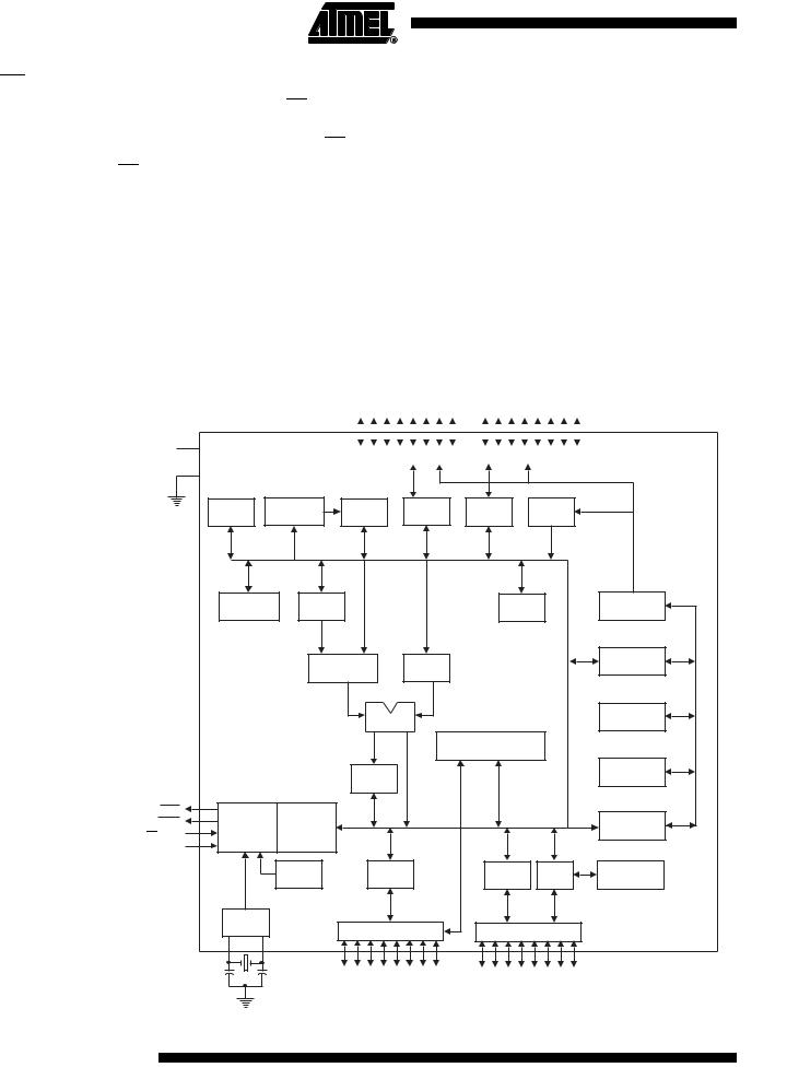
4. Block Diagram
VCC
GND
PSEN
ALE/PROG
EA / VPP
RST
6 AT89S8253
|
|
P0.0 - P0.7 |
|
|
P2.0 - P2.7 |
|||||||||||||
|
|
|
|
|
|
|
|
|
|
|
|
|
|
|
|
|
|
|
|
|
|
|
|
|
|
|
|
|
|
|
|
|
|
|
|
|
|
|
|
|
|
|
|
|
|
|
|
|
|
|
|
|
|
|
|
|
|
PORT 0 DRIVERS |
|
|
PORT 2 DRIVERS |
||||||||||||||
|
|
|
|
|
|
|
|
|
|
|
|
|
|
|
|
|
|
|
EEPROM |
RAM ADDR. |
RAM |
PORT 0 |
PORT 2 |
FLASH |
|
REGISTER |
LATCH |
LATCH |
|
|||
B |
|
|
|
STACK |
PROGRAM |
|
ACC |
|
|
ADDRESS |
|||
REGISTER |
|
|
POINTER |
|||
|
|
REGISTER |
||||
|
|
|
|
|
|
|
|
|
|
|
|
|
BUFFER |
|
TMP2 |
|
TMP1 |
|
|
|
|
|
|
|
|
|
PC |
|
|
ALU |
|
|
INCREMENTER |
|
|
|
|
INTERRUPT, SERIAL PORT, |
|
||
|
|
|
|
AND TIMER BLOCKS |
|
|
|
|
|
|
|
|
PROGRAM |
|
|
PSW |
|
|
|
COUNTER |
|
|
|
|
|
|
|
TIMING |
INSTRUCTION |
|
|
|
|
DUAL |
AND |
|
|
|
|
||
REGISTER |
|
|
|
|
DPTR |
|
CONTROL |
|
|
|
|
||
|
|
|
|
|
|
|
|
WATCH |
PORT 3 |
PORT 1 |
SPI |
PROGRAM |
|
|
DOG |
LATCH |
LATCH |
PORT |
LOGIC |
|
OSC |
|
|
|
|
|
|
|
|
PORT 3 DRIVERS |
PORT 1 DRIVERS |
|
||
|
|
P3.0 |
- P3.7 |
P1.0 |
- P1.7 |
|
|
|
|
|
|
||
|
|
|
|
|
|
3286K–MICRO–12/06 |

AT89S8253
5. Special Function Registers
A map of the on-chip memory area called the Special Function Register (SFR) space is shown in
Table 5-1.
Note that not all of the addresses are occupied, and unoccupied addresses may not be implemented on the chip. Read accesses to these addresses will generally return random data, and write accesses will have an indeterminate effect.
User software should not write 1s to these unlisted locations, since they may be used in future products to invoke new features. In that case, the reset or inactive values of the new bits will always be 0.
Table 5-1. |
AT89S8253 SFR Map and Reset Values |
|
|
|
|
|
||||
0F8H |
|
|
|
|
|
|
|
|
|
0FFH |
|
|
|
|
|
|
|
|
|
|
|
0F0H |
|
B |
|
|
|
|
|
|
|
0F7H |
|
00000000 |
|
|
|
|
|
|
|
||
|
|
|
|
|
|
|
|
|
|
|
0E8H |
|
|
|
|
|
|
|
|
|
0EFH |
|
|
|
|
|
|
|
|
|
||
|
|
|
|
|
|
|
|
|
|
|
0E0H |
|
ACC |
|
|
|
|
|
|
|
0E7H |
|
00000000 |
|
|
|
|
|
|
|
||
|
|
|
|
|
|
|
|
|
|
|
0D8H |
|
|
|
|
|
|
|
|
|
0DFH |
|
|
|
|
|
|
|
|
|
||
|
|
|
|
|
|
|
|
|
|
|
0D0H |
|
PSW |
|
|
|
|
SPCR |
|
|
0D7H |
|
00000000 |
|
|
|
|
00000100 |
|
|
||
|
|
|
|
|
|
|
|
|
||
|
|
|
|
|
|
|
|
|
|
|
0C8H |
|
T2CON |
T2MOD |
RCAP2L |
RCAP2H |
TL2 |
TH2 |
|
|
0CFH |
|
00000000 |
XXXXXX00 |
00000000 |
00000000 |
00000000 |
00000000 |
|
|
||
|
|
|
|
|
||||||
0C0H |
|
|
|
|
|
|
|
|
|
0C7H |
|
|
|
|
|
|
|
|
|
||
|
|
|
|
|
|
|
|
|
|
|
0B8H |
|
IP |
SADEN |
|
|
|
|
|
|
0BFH |
|
XX000000 |
00000000 |
|
|
|
|
|
|
||
|
|
|
|
|
|
|
|
|
||
|
|
|
|
|
|
|
|
|
|
|
0B0H |
|
P3 |
|
|
|
|
|
|
IPH |
0B7H |
|
11111111 |
|
|
|
|
|
|
XX000000 |
||
|
|
|
|
|
|
|
|
|
||
|
|
|
|
|
|
|
|
|
|
|
0A8H |
|
IE |
SADDR |
SPSR |
|
|
|
|
|
0AFH |
|
0X000000 |
00000000 |
000XXX00 |
|
|
|
|
|
||
|
|
|
|
|
|
|
|
|||
|
|
|
|
|
|
|
|
|
|
|
0A0H |
|
P2 |
|
|
|
|
|
WDTRST |
WDTCON |
0A7H |
|
11111111 |
|
|
|
|
|
(Write Only) |
0000 0000 |
||
|
|
|
|
|
|
|
|
|||
|
|
|
|
|
|
|
|
|
|
|
98H |
|
SCON |
SBUF |
|
|
|
|
|
|
9FH |
|
00000000 |
XXXXXXXX |
|
|
|
|
|
|
||
|
|
|
|
|
|
|
|
|
||
|
|
|
|
|
|
|
|
|
|
|
90H |
|
P1 |
|
|
|
|
|
EECON |
|
97H |
|
11111111 |
|
|
|
|
|
XX000011 |
|
||
|
|
|
|
|
|
|
|
|
||
|
|
|
|
|
|
|
|
|
|
|
88H |
|
TCON |
TMOD |
TL0 |
TL1 |
TH0 |
TH1 |
AUXR |
CLKREG |
8FH |
|
00000000 |
00000000 |
00000000 |
00000000 |
00000000 |
00000000 |
XXXXXXX0 |
XXXXXXX0 |
||
|
|
|
||||||||
|
|
|
|
|
|
|
|
|
|
|
80H |
|
P0 |
SP |
DP0L |
DP0H |
DP1L |
DP1H |
SPDR |
PCON |
87H |
|
11111111 |
00000111 |
00000000 |
00000000 |
00000000 |
00000000 |
######## |
00XX0000 |
||
|
|
|
||||||||
|
|
|
|
|
|
|
|
|
|
|
Note: # means: 0 after cold reset and unchanged after warm reset.
7
3286K–MICRO–12/06
5.1Auxiliary Register
The AUXR Register contains a single active bit called DISALE.
Table 5-2. |
|
AUXR – Auxiliary Register |
|
|
|
|
|
|
|||
AUXR Address = 8EH |
|
|
|
|
Reset Value = XXXX XXX0B |
||||||
Not Bit Addressable |
|
|
|
|
|
|
|
||||
|
|
|
|
|
|
|
|
|
|
|
|
|
|
– |
|
– |
– |
– |
– |
– |
Intel_Pwd_Exit |
DISALE |
|
|
|
|
|
|
|
|
|
|
|
|
|
Bit |
|
7 |
|
6 |
5 |
4 |
3 |
2 |
1 |
0 |
|
|
|
|
|
|
|
|
|
|
|
|
|
|
|
|
|
|
|
|
|
|
|
|
|
Symbol |
|
|
Function |
|
|
|
|
|
|
|
|
When set, this bit configures the interrupt driven exit from power-down to resume execution on the rising edge of Intel_Pwd_Exit the interrupt signal. When this bit is cleared, the execution resumes after a self-timed interval (nominal 2 ms)
referenced from the falling edge of the interrupt signal.
DISALE
When DISALE = 0, ALE is emitted at a constant rate of 1/6 the oscillator frequency (except during MOVX when 1 ALE pulse is missing). When DISALE = 1, ALE is active only during a MOVX or MOVC instruction.
5.2Clock Register
The CLKREG register contains a single active bit called X2.
Table 5-3. |
|
CLKREG – Clock Register |
|
|
|
|
|
|
|
|||
CLKREG Address = 8FH |
|
|
|
|
Reset Value = XXXX XXX0B |
|||||||
Not Bit Addressable |
|
|
|
|
|
|
|
|
||||
|
|
|
|
|
|
|
|
|
|
|
|
|
|
|
– |
|
– |
– |
– |
– |
– |
|
– |
X2 |
|
|
|
|
|
|
|
|
|
|
|
|
|
|
Bit |
|
7 |
|
6 |
5 |
4 |
3 |
2 |
|
1 |
0 |
|
|
|
|
|
|
|
|
|
|
|
|
|
|
|
|
|
|
|
|
|
|
|
|
|
||
Symbol |
|
Function |
|
|
|
|
|
|
|
|
||
When X2 = 0, the oscillator frequency (at XTAL1 pin) is internally divided by 2 before it is used as the device system
frequency.
X2
When X2 = 1, the divider by 2 is no longer used and the XTAL1 frequency becomes the device system frequency. This enables the user to choose a 6 MHz crystal instead of a 12 MHz crystal, for example, in order to reduce EMI.
5.3SPI Registers
Control and status bits for the Serial Peripheral Interface are contained in registers SPCR (see Table 14-1 on page 25) and SPSR (see Table 14-2 on page 26). The SPI data bits are contained in the SPDR register. In normal SPI mode, writing the SPI data register during serial data transfer sets the Write Collision bit (WCOL) in the SPSR register. In enhanced SPI mode, the SPDR is also write double-buffered because WCOL works as a Write Buffer Full Flag instead of being a collision flag. The values in SPDR are not changed by Reset.
5.4Interrupt Registers
The global interrupt enable bit and the individual interrupt enable bits are in the IE register. In addition, the individual interrupt enable bit for the SPI is in the SPCR register. Four priorities can be set for each of the six interrupt sources in the IP and IPH registers.
IPH bits have the same functions as IP bits, except IPH has higher priority than IP. By using IPH in conjunction with IP, a priority level of 0, 1, 2, or 3 may be set for each interrupt.
8 AT89S8253 
3286K–MICRO–12/06

AT89S8253
5.5Dual Data Pointer Registers
To facilitate accessing both internal EEPROM and external data memory, two banks of 16-bit Data Pointer Registers are provided: DP0 at SFR address locations 82H - 83H and DP1 at 84H - 85H. Bit DPS = 0 in SFR EECON selects DP0 and DPS = 1 selects DP1. The user should ALWAYS initialize the DPS bit to the appropriate value before accessing the respective Data Pointer Register.
5.6Power Off Flag
The Power Off Flag (POF), located at bit_4 (PCON.4) in the PCON SFR. POF, is set to “1” during power up. It can be set and reset under software control and is not affected by RESET.
6. Data Memory – EEPROM and RAM
The AT89S8253 implements 2K bytes of on-chip EEPROM for data storage and 256 bytes of RAM. The upper 128 bytes of RAM occupy a parallel space to the Special Function Registers. That means the upper 128 bytes have the same addresses as the SFR space but are physically separate from SFR space.
When an instruction accesses an internal location above address 7FH, the address mode used in the instruction specifies whether the CPU accesses the upper 128 bytes of RAM or the SFR space. Instructions that use direct addressing access the SFR space.
For example, the following direct addressing instruction accesses the SFR at location 0A0H (which is P2).
MOV 0A0H, #data
Instructions that use indirect addressing access the upper 128 bytes of RAM. For example, the following indirect addressing instruction, where R0 contains 0A0H, accesses the data byte at address 0A0H, rather than P2 (whose address is 0A0H).
MOV @R0, #data
Note that stack operations are examples of indirect addressing, so the upper 128 bytes of data
RAM are available as stack space.
The on-chip EEPROM data memory is selected by setting the EEMEN bit in the EECON register at SFR address location 96H. The EEPROM address range is from 000H to 7FFH. MOVX instructions are used to access the EEPROM. To access off-chip data memory with the MOVX instructions, the EEMEN bit needs to be set to “0”.
During program execution mode (using the MOVX instruction) there is an auto-erase capability at the byte level. This means that the user can update or modify a single EEPROM byte location in real-time without affecting any other bytes.
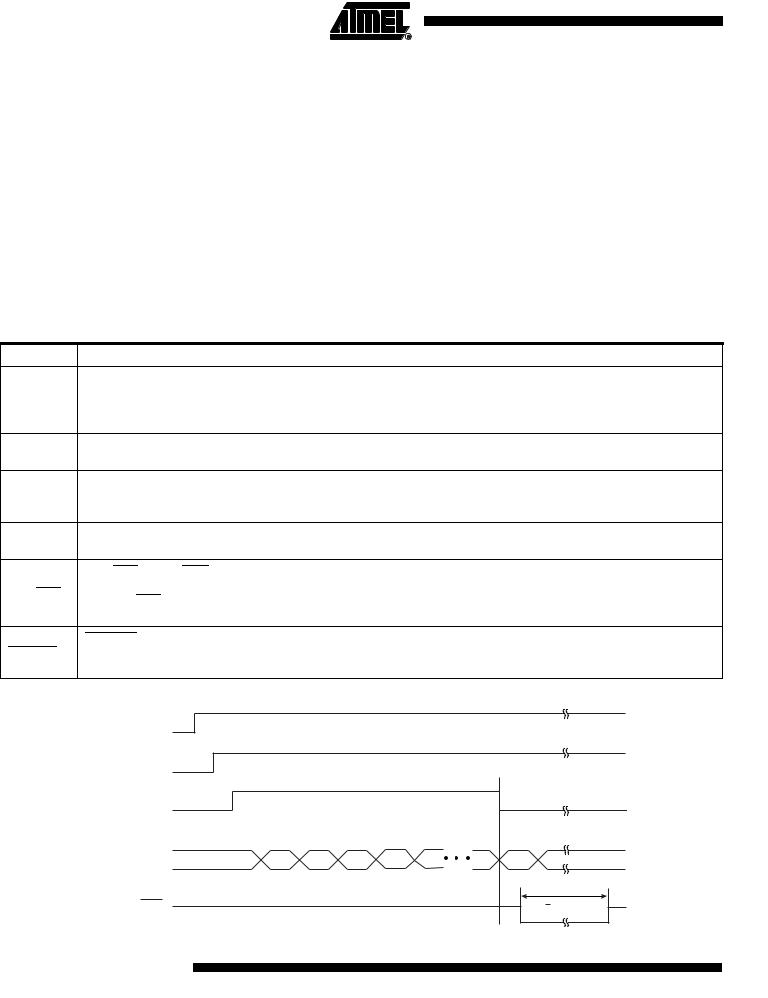
The EEMWE bit in the EECON register needs to be set to “1” before any byte location in the EEPROM can be written. User software should reset EEMWE bit to “0” if no further EEPROM write is required. EEPROM write cycles in the serial programming mode are self-timed and typically take 4 ms. The progress of EEPROM write can be monitored by reading the RDY/BSY bit (read-only) in SFR EECON. RDY/BSY = 0 means programming is still in progress and RDY/BSY = 1 means an EEPROM write cycle is completed and another write cycle can be initiated. Bit EELD in EECON controls whether the next MOVX instruction will only load the write buffer of the EEPROM or will actually start the programming cycle. By setting EELD, only load will occur. Before the last MOVX in a given page of 32 bytes, EELD should be cleared so that after the last MOVX the entire page will be programmed at the same time. This way, 32 bytes will only require 4 ms of programming time instead of 128 ms required in single byte programming.
9
3286K–MICRO–12/06
In addition, during EEPROM programming, an attempted read from the EEPROM will fetch the byte being written with the MSB complemented. Once the write cycle is completed, true data are valid at all bit locations.
6.1Memory Control Register
The EECON register contains control bits for the 2K bytes of on-chip data EEPROM. It also contains the control bit for the dual data pointer.
Table 6-1. |
EECON – Data EEPROM Control Register |
|
|
|
|
|
|
|
|
|
|||
EECON Address = 96H |
|
|
|
|
|
Reset Value = XX00 0011B |
|||||||
Not Bit Addressable |
|
|
|
|
|
|
|
|
|
|
|
|
|
|
|
|
|
|
|
|
|
|
|
|
|
|
|
|
|
|
|
|
|
|
|
|
|
|
|
|
|
Bit |
– |
– |
EELD |
EEMWE |
EEMEN |
DPS |
|
|
|
|
|
|
|
RDY/BSY |
|
|
WRTINH |
|
|||||||||
|
|
|
|
|
|
|
|
|
|
|
|
||
|
7 |
6 |
5 |
4 |
3 |
2 |
1 |
|
0 |
|
|
||
|
|
|
|
|
|
|
|
|
|
|
|
|
|
Symbol Function
EEPROM data memory load enable bit. Used to implement Page Mode Write. A MOVX instruction writing into the data
EELD
EEPROM will not initiate the programming cycle if this bit is set, rather it will just load data into the volatile data buffer of the data EEPROM memory. Before the last MOVX, reset this bit and the data EEPROM will program all the bytes previously loaded on the same page of the address given by the last MOVX instruction.
EEMWE
EEPROM data memory write enable bit. Set this bit to 1 before initiating byte write to on-chip EEPROM with the MOVX instruction. User software should set this bit to 0 after EEPROM write is completed.
Internal EEPROM access enable. When EEMEN = 1, the MOVX instruction with DPTR will access on-chip EEPROM EEMEN instead of external data memory if the address used is less than 2K. When EEMEN = 0 or the address used is ≥ 2K,
MOVX with DPTR accesses external data memory.
DPS
Data pointer register select. DPS = 0 selects the first bank of data pointer register, DP0, and DPS = 1 selects the second bank, DP1.
RDY/BSY (Ready/Busy) flag for the data EEPROM memory. This is a read-only bit which is cleared by hardware during
RDY/BSY
the programming cycle of the on-chip EEPROM. It is also set by hardware when the programming is completed. Note
that RDY/BSY will be cleared long after the completion of the MOVX instruction which has initiated the programming cycle.
WRTINH (Write Inhibit) is a READ-ONLY bit which is cleared by hardware when Vcc is too low for the programming cycle WRTINH of the on-chip EEPROM to be executed. When this bit is cleared, an ongoing programming cycle will be aborted or a
new programming cycle will not start.
Figure 6-1. Data EEPROM Write Sequence
EEMEN |
|
|
|
|
|
|
EEMWE |
|
|
|
|
|
|
EELD |
|
|
|
|
|
|
MOVX DATA |
0 |
1 |
2 |
3 |
30 |
31 |
RDY/BSY |
|
|
|
|
|
~ 4 ms |
10 AT89S8253
3286K–MICRO–12/06
AT89S8253
7. Power-On Reset
A Power-On Reset (POR) is generated by an on-chip detection circuit. The detection level is nominally 1.4V. The POR is activated whenever VCC is below the detection level. The POR circuit can be used to trigger the start-up reset or to detect a supply voltage failure in devices without a brown-out detector. The POR circuit ensures that the device is reset from power-on. When VCC reaches the Power-on Reset threshold voltage, the POR delay counter determines how long the device is kept in POR after VCC rise, nominally 2 ms. The POR signal is activated again, without any delay, when VCC falls below the POR threshold level. A Power-On Reset (i.e. a cold reset) will set the POF flag in PCON.
Figure 7-1. Power-up and Brown-out Detection Sequence
VCC
Min VCC Level 2.7V |
|
|
BOD Level 2.3V |
|
|
POR Level 1.4V |
|
|
|
|
t |
POR |
|
|
|
|
t |
XTAL1 |
|
2.4V |
|
1.2V |
|
|
|
|
|
|
t |
BOD |
|
|
|
|
t |
Internal |
|
|
RESET |
tPOR |
tPOR |
|
||
|
(2 ms) |
(2 ms) |
|
|
t |
|
0 |
|
7.1Brown-out Reset
The AT89S8253 has an on-chip Brown-out Detection (BOD) circuit for monitoring the VCC level during operation by comparing it to a fixed trigger level of 2.4V (max). The trigger level for the BOD is nominally 2.2V. The purpose of the BOD is to ensure that if VCC fails or dips while executing at speed, the system will gracefully enter reset without the possibility of errors induced by incorrect execution. When VCC decreases to a value below the trigger level, the Brown-out Reset is immediately activated. When VCC increases above the trigger level, the BOD delay counter starts the MCU after the timeout period has expired in approximately 2 ms.
11
3286K–MICRO–12/06

8. Programmable Watchdog Timer
The programmable Watchdog Timer (WDT) counts instruction cycles. The prescaler bits, PS0, PS1 and PS2 in SFR WDTCON are used to set the period of the Watchdog Timer from 16K to 2048K instruction cycles. The available timer periods are shown in Table 8-1. The WDT time-out
period is dependent upon the external clock frequency.
The WDT is disabled by Power-on Reset and during Power-down mode. When WDT times out without being serviced or disabled, an internal RST pulse is generated to reset the CPU. See Table 8-1 for the WDT period selections.
Table 8-1. |
Watchdog Timer Time-out Period Selection |
|
||
|
|
WDT Prescaler Bits |
|
Period (Nominal for |
|
|
|
|
|
PS2 |
|
PS1 |
PS0 |
FCLK = 12 MHz) |
0 |
|
0 |
0 |
16 ms |
|
|
|
|
|
0 |
|
0 |
1 |
32 ms |
|
|
|
|
|
0 |
|
1 |
0 |
64 ms |
|
|
|
|
|
0 |
|
1 |
1 |
128 ms |
|
|
|
|
|
1 |
|
0 |
0 |
256 ms |
|
|
|
|
|
1 |
|
0 |
1 |
512 ms |
|
|
|
|
|
1 |
|
1 |
0 |
1024 ms |
|
|
|
|
|
1 |
|
1 |
1 |
2048 ms |
|
|
|
|
|
12 AT89S8253 
3286K–MICRO–12/06
AT89S8253
8.1Watchdog Control Register
The WDTCON register contains control bits for the Watchdog Timer (shown in Table 8-2).
Table 8-2. |
WDTCON – Watchdog Control Register |
|
|
|
|
|
||||
WDTCON Address = A7H |
|
|
|
|
Reset Value = 0000 0000B |
|||||
Not Bit Addressable |
|
|
|
|
|
|
|
|
||
|
|
|
|
|
|
|
|
|
|
|
|
|
PS2 |
PS1 |
PS0 |
WDIDLE |
DISRTO |
HWDT |
WSWRST |
WDTEN |
|
|
|
|
|
|
|
|
|
|
|
|
Bit |
|
7 |
6 |
5 |
4 |
3 |
2 |
1 |
0 |
|
|
|
|
|
|
|
|
|
|
|
|
Symbol Function
PS2
Prescaler bits for the watchdog timer (WDT). When all three bits are cleared to 0, the watchdog timer has a nominal
PS1
period of 16K machine cycles, (i.e. 16 ms at a XTAL frequency of 12 MHz in normal mode or 6 MHz in x2 mode). When
PS0
all three bits are set to 1, the nominal period is 2048K machine cycles, (i.e. 2048 ms at 12 MHz clock frequency in normal mode or 6 MHz in x2 mode).
WDIDLE
Enable/disable the Watchdog Timer in IDLE mode. When WDIDLE = 0, WDT continues to count in IDLE mode. When WDIDLE = 1, WDT freezes while the device is in IDLE mode.
Enable/disable the WDT-driven Reset Out (WDT drives the RST pin). When DISRTO = 0, the RST pin is driven high DISRTO after WDT times out and the entire board is reset. When DISRTO = 1, the RST pin remains only as an input and the
WDT resets only the microcontroller internally after WDT times out.
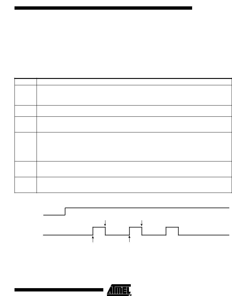
Hardware mode select for the WDT. When HWDT = 0, the WDT can be turned on/off by simply setting or clearing WDTEN in the same register (this is the software mode for WDT). When HWDT = 1, the WDT has to be set by writing
HWDT
the sequence 1EH/E1H to the WDTRST register (with address 0A6H) and after being set in this way, WDT cannot be turned off except by reset, warm or cold (this is the hardware mode for WDT). To prevent the hardware WDT from resetting the entire device, the same sequence 1EH/E1H must be written to the same WDTRST SFR before the timeout interval.
Watchdog software reset bit. If HWDT = 0 (i.e. WDT is in software controlled mode), when set by software, this bit resets WSWRST WDT. After being set by software, WSWRST is reset by hardware during the next machine cycle. If HWDT = 1, this bit
has no effect, and if set by software, it will not be cleared by hardware.
Watchdog software enable bit. When HWDT = 0 (i.e. WDT is in software-controlled mode), this bit enables WDT when WDTEN set to 1 and disables WDT when cleared to 0 (it does not reset WDT in this case, but just freezes the existing counter
state). If HWDT = 1, this bit is READ-ONLY and reflects the status of the WDT (whether it is running or not).
Figure 8-1. Software Mode – Watchdog Timer Sequence
WDTEN |
HW |
HW |
|
WSWRST
SW Writes a 1 |
SW |
13
3286K–MICRO–12/06

9. Timer 0 and 1
Timer 0 and Timer 1 in the AT89S8253 operate the same way as Timer 0 and Timer 1 in the AT89S51 and AT89S52. For more detailed information on the Timer/Counter operation, please click on the document link below:
http://www.atmel.com/dyn/resources/prod_documents/DOC4316.PDF
10. Timer 2
Timer 2 is a 16-bit Timer/Counter that can operate as either a timer or an event counter. The type of operation is selected by bit C/T2 in the SFR T2CON (see Table 10-2 on page 15). Timer 2 has three operating modes: capture, auto-reload (up or down counting), and baud rate generator. The modes are selected by bits in T2CON, as shown in Table 10-2.
Timer 2 consists of two 8-bit registers, TH2 and TL2. In the Timer function, the TL2 register is incremented every machine cycle. Since a machine cycle consists of 12 oscillator periods, the count rate is 1/12 of the oscillator frequency.
In the Counter function, the register is incremented in response to a 1-to-0 transition at its corresponding external input pin, T2. In this function, the external input is sampled during S5P2 of every machine cycle. When the samples show a high in one cycle and a low in the next cycle, the count is incremented. The new count value appears in the register during S3P1 of the cycle following the one in which the transition was detected. Since two machine cycles (24 oscillator periods) are required to recognize a 1-to-0 transition, the maximum count rate is 1/24 of the oscillator frequency. To ensure that a given level is sampled at least once before it changes, the level should be held for at least one full machine cycle.
Table 10-1. Timer 2 Operating Modes
|
|
|
|
|
|
RCLK + TCLK |
CP/RL2 |
TR2 |
MODE |
||
|
|
|
|
|
|
0 |
0 |
|
1 |
16-bit Auto-reload |
|
|
|
|
|
|
|
0 |
1 |
|
1 |
16-bit Capture |
|
|
|
|
|
|
|
1 |
X |
1 |
Baud Rate Generator |
||
|
|
|
|
|
|
X |
X |
0 |
(Off) |
||
|
|
|
|
|
|
14 AT89S8253 
3286K–MICRO–12/06

 AT89S8253
Table 10-2. T2CON – Timer/Counter 2 Control Register
T2CON Address = 0C8H |
|
|
|
|
|
Reset Value = 0000 0000B |
|||||||
Bit Addressable |
|
|
|
|
|
|
|
|
|
|
|
||
|
|
|
|
|
|
|
|
|
|
|
|
|
|
|
TF2 |
|
EXF2 |
RCLK |
TCLK |
EXEN2 |
TR2 |
|
|
|
|
|
|
|
C/T2 |
|
CP/RL2 |
||||||||||
|
|
|
|
|
|
|
|
|
|
|
|
||
Bit |
7 |
|
6 |
5 |
4 |
3 |
2 |
1 |
|
0 |
|
||
|
|
|
|
|
|
|
|
|
|
|
|
|
|
Symbol Function
TF2
Timer 2 overflow flag set by a Timer 2 overflow and must be cleared by software. TF2 will not be set when either RCLK = 1 or TCLK = 1.
Timer 2 external flag set when either a capture or reload is caused by a negative transition on T2EX and EXEN2 = 1. EXF2 When Timer 2 interrupt is enabled, EXF2 = 1 will cause the CPU to vector to the Timer 2 interrupt routine. EXF2 must be
cleared by software. EXF2 does not cause an interrupt in up/down counter mode (DCEN = 1).
RCLK
Receive clock enable. When set, causes the serial port to use Timer 2 overflow pulses for its receive clock in serial port Modes 1 and 3. RCLK = 0 causes Timer 1 overflows to be used for the receive clock.
TCLK
Transmit clock enable. When set, causes the serial port to use Timer 2 overflow pulses for its transmit clock in serial port Modes 1 and 3. TCLK = 0 causes Timer 1 overflows to be used for the transmit clock.
EXEN2
Timer 2 external enable. When set, allows a capture or reload to occur as a result of a negative transition on T2EX if Timer 2 is not being used to clock the serial port. EXEN2 = 0 causes Timer 2 to ignore events at T2EX.
TR2 |
Start/Stop control for Timer 2. TR2 = 1 starts the timer. |
C/T2
Timer or counter select for Timer 2. C/T2 = 0 for timer function. C/T2 = 1 for external event counter (falling edge triggered).
Capture/Reload select. CP/RL2 = 1 causes captures to occur on negative transitions at T2EX if EXEN2 = 1. CP/RL2 = 0 CP/RL2 causes automatic reloads to occur when Timer 2 overflows or negative transitions occur at T2EX when EXEN2 = 1. When
either RCLK or TCLK = 1, this bit is ignored and the timer is forced to auto-reload on Timer 2 overflow.
10.1Timer 2 Registers
Control and status bits are contained in registers T2CON (see Table 10-2) and T2MOD (see Table 10-3) for Timer 2. The register pair (RCAP2H, RCAP2L) are the Capture/Reload registers for Timer 2 in 16-bit capture mode or 16-bit auto-reload mode.
10.2Capture Mode
In the capture mode, two options are selected by bit EXEN2 in T2CON. If EXEN2 = 0, Timer 2 is a 16-bit timer or counter which upon overflow sets bit TF2 in T2CON. This bit can then be used to generate an interrupt. If EXEN2 = 1, Timer 2 performs the same operation, but a 1-to-0 transition at external input T2EX also causes the current value in TH2 and TL2 to be captured into RCAP2H and RCAP2L, respectively. In addition, the transition at T2EX causes bit EXF2 in T2CON to be set. The EXF2 bit, like TF2, can generate an interrupt. The capture mode is illustrated in Figure 10-1.
15
3286K–MICRO–12/06
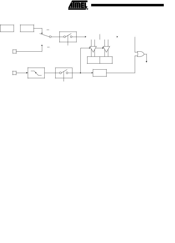
Figure 10-1. Timer 2 in Capture Mode
OSC  ÷12
÷12
C/T2 = 0
TH2 |
TL2 |
|
|
TF2 |
|
|
|
|
|||
|
|
|
|
|
|
OVERFLOW
CONTROL
TR2
C/T2 = 1
T2 PIN |
CAPTURE |
|
RCAP2H RCAP2L
TRANSITION
DETECTOR TIMER 2
INTERRUPT
T2EX PIN |
EXF2 |
CONTROL
EXEN2
10.3Auto-reload (Up or Down Counter)
Timer 2 can be programmed to count up or down when configured in its 16-bit auto-reload mode. This feature is invoked by the DCEN (Down Counter Enable) bit located in the SFR T2MOD (see Table 10-3). Upon reset, the DCEN bit is set to 0 so that timer 2 will default to count up. When DCEN is set, Timer 2 can count up or down, depending on the value of the T2EX pin.
Table 10-3. T2MOD – Timer 2 Mode Control Register
T2MOD Address = 0C9H |
|
|
|
|
|
|
|
|
Reset Value = XXXX XX00B |
|
||||
Not Bit Addressable |
|
|
|
|
|
|
|
|
|
|
|
|||
|
|
|
|
|
|
|
|
|
|
|
|
|
|
|
|
|
– |
|
– |
|
– |
|
– |
– |
|
– |
T2OE |
DCEN |
|
|
|
|
|
|
|
|
|
|
|
|
|
|
|
|
Bit |
|
7 |
|
6 |
|
5 |
|
4 |
3 |
|
2 |
1 |
0 |
|
|
|
|
|
|
|
|
|
|
|
|
|
|
|
|
|
|
|
|
|
|
|
|
|
|
|
|
|
||
Symbol |
Function |
|
|
|
|
|
|
|
|
|
|
|
||
|
|
|
|
|
|
|
|
|
||||||
– |
Not implemented, reserved for future use. |
|
|
|
|
|
|
|
||||||
|
|
|
|
|
|
|
|
|
|
|
||||
T2OE |
Timer 2 Output Enable bit. |
|
|
|
|
|
|
|
|
|
||||
|
|
|
|
|
|
|||||||||
DCEN |
When set, this bit allows Timer 2 to be configured as an up/down counter. |
|
|
|
|
|||||||||
|
|
|
|
|
|
|
|
|
|
|
|
|
|
|
Figure 10-2 shows Timer 2 automatically counting up when DCEN = 0. In this mode, two options are selected by bit EXEN2 in T2CON. If EXEN2 = 0, Timer 2 counts up to 0FFFFH and then sets the TF2 bit upon overflow. The overflow also causes the timer registers to be reloaded with the 16-bit value in RCAP2H and RCAP2L. The values in RCAP2H and RCAP2L are preset by software. If EXEN2 = 1, a 16-bit reload can be triggered either by an overflow or by a 1-to-0 transition at external input T2EX. This transition also sets the EXF2 bit. Both the TF2 and EXF2 bits can generate an interrupt if enabled.
Setting the DCEN bit enables Timer 2 to count up or down, as shown in Figure 10-3. In this mode, the T2EX pin controls the direction of the count. A logic 1 at T2EX makes Timer 2 count up. The timer will overflow at 0FFFFH and set the TF2 bit. This overflow also causes the 16-bit value in RCAP2H and RCAP2L to be reloaded into the timer registers, TH2 and TL2, respectively.
16 AT89S8253 
3286K–MICRO–12/06

 AT89S8253
A logic 0 at T2EX makes Timer 2 count down. The timer underflows when TH2 and TL2 equal the values stored in RCAP2H and RCAP2L. The underflow sets the TF2 bit and causes 0FFFFH to be reloaded into the timer registers.
The EXF2 bit toggles whenever Timer 2 overflows or underflows and can be used as a 17th bit of resolution. In this operating mode, EXF2 does not flag an interrupt.
Figure 10-2. Timer 2 in Auto Reload Mode (DCEN = 0)
Figure 10-3. Timer 2 Auto Reload Mode (DCEN = 1 Timer 2 Auto Reload Mode (DCEN = 1)
17
3286K–MICRO–12/06
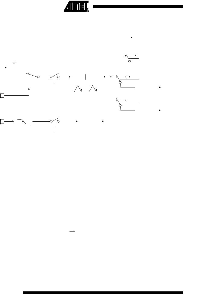
Figure 10-4. Timer 2 in Baud Rate Generator Mode
TIMER 1 OVERFLOW
|
|
|
|
|
|
|
|
|
|
|
|
|
|
|
|
|
|
|
|
|
|
|
|
|
|
|
|
|
|
|
|
|
|
|
|
|
|
|
|
|
|
|
|
|
|
|
|
|
|
|
|
|
|
|
|
|
|
|
|
|
|
|
|
|
|
|
|
|
|
|
|
|
|
|
|
|
|
|
|
|
|
|
|
|
|
|
|
|
|
|
|
|
|
|
|
|
|
|
|
|
|
|
|
|
|
|
|
|
|
|
|
|
|
|
|
|
|
|
|
|
|
|
÷2 |
|
|
|
|
|
|
|
|
|
|
|
|
||
|
|
|
|
|
|
|
|
|
|
|
|
|
|
|
|
|
|
|
|
|
|
|
|
|
|
|
|
|
|
|
|
|
|
|
|
"0" |
"1" |
|
|
|
|||||
|
|
|
|
|
|
NOTE: OSC. FREQ. IS DIVIDED BY 2, NOT 12 |
|
|
|
|
|
|
|
|
|
|
|
|
|
|
|
|
|
||||||||||||||||||||||
|
|
|
|
|
|
|
|
|
|
|
|
|
|
|
|
|
|
|
|
SMOD1 |
|||||||||||||||||||||||||
|
|
|
|
|
|
|
|
|
|
|
|
|
|
|
|
|
|
|
|
|
|
|
|
|
|
|
|
|
|
|
|
|
|
|
|
|
|
|
|
|
|
|
|||
|
|
|
|
|
|
|
|
|
|
|
|
|
|
|
|
|
|
|
|
|
|
|
|
|
|
|
|
|
|
|
|
|
|
|
|
|
|
|
|
|
|
|
|
|
|
|
OSC |
|
|
÷2 |
|
|
|
|
|
|
|
|
|
|
|
|
|
|
|
|
|
|
|
|
|
|
|
|
|
|
|
|
|
|
|
|
|
|
|
|
|
|
|
|
|
|
|
|
|
C/T2 = 0 |
|
|
|
|
|
|
|
|
|
|
|
|
|
|
|
|
|
|
|
"1" |
|
"0" |
|
|
|
|
|
|
|
||||||||||||
|
|
|
|
|
|
|
|
|
|
|
|
|
|
|
|
TH2 |
|
TL2 |
|
|
|
|
|
|
|
|
|
|
|
|
|
|
RCLK |
||||||||||||
|
|
|
|
|
|
|
|
|
|
|
|
|
|
|
|
|
|
|
|
|
|
|
|
|
|
|
|
|
|
|
|||||||||||||||
|
|
|
|
|
|
|
|
|
|
|
|
|
|
|
|
|
|
|
|
|
|
|
|
|
|
|
|
|
|
|
|
|
|
|
|
|
|
|
|
|
|
|
|||
|
|
|
|
|
|
|
|
|
|
|
|
|
|
|
|
|
|
|
|
|
|
|
|
|
|
|
|
|
|
|
|
|
|
|
|
|
|
|
|
|
|
|
|
Rx |
|
|
|
|
|
|
|
|
|
|
|
|
CONTROL |
|
|
|
|
|
|
|
|
|
|
|
|
|
|
|
|
|
|
|
|
|
|
|
|
÷16 |
CLOCK |
||||||||
|
|
|
|
|
|
|
|
|
|
TR2 |
|
|
|
|
|
|
|
|
|
|
|
|
|
|
|
|
|
|
|
|
|
|
|
|
|
|
|||||||||
|
|
|
|
|
|
|
|
|
|
|
|
|
|
|
|
|
|
|
|
|
|
|
|
|
|
|
|
|
|
|
|
|
|
|
|
||||||||||
|
|
|
|
|
|
|
|
|
|
|
|
|
|
|
|
|
|
|
|
|
|
|
|
|
|
|
|
|
|
|
|
|
|
|
|
||||||||||
|
|
|
|
|
|
|
|
|
|
|
|
|
|
|
|
|
|
|
|
|
|
|
|
|
|
|
|
|
|
|
|
|
|
|
|
|
|
|
|
|
|
|
|
|
|
|
|
|
|
|
|
|
C/T2 = 1 |
|
|
|
|
|
|
|
|
|
|
|
|
|
|
|
"1" |
|
"0" |
|
|
|
|
|
|
|
|||||||||||||
|
|
|
|
|
|
|
|
|
|
|
|
|
|
|
|
|
|
|
|
|
|
|
|
|
|
|
|
|
|
||||||||||||||||
|
|
|
|
|
|
|
|
|
|
|
|
|
|
|
|
|
|
|
|
|
|
|
|
|
|
|
|
|
|
|
|
|
|
|
|
|
|
|
|||||||
|
T2 PIN |
|
|
|
|
|
|
|
|
|
|
|
|
|
|
|
|
|
|
|
|
|
|
|
|
|
|
|
|
|
|
|
|
|
|
|
|
|
|
|
TCLK |
||||
|
|
|
|
|
|
|
|
|
|
|
|
|
|
|
|
|
|
|
|
|
|
|
|
|
|
|
|
|
|
|
|
|
|
|
|
|
|
|
|
||||||
|
|
|
|
|
|
|
|
|
|
|
|
|
|
|
|
RCAP2H |
RCAP2L |
|
|
|
|
|
|
|
|
|
|
|
|
|
|
|
|||||||||||||
|
|
|
|
|
|
|
|
|
|
|
|
|
|
|
|
|
|
|
|
|
|
|
|
|
|
|
|
|
|
|
|
Tx |
|||||||||||||
|
|
|
|
|
|
|
|
|
|
|
|
|
|
|
|
|
|
|
|
|
|
|
|
|
|
|
|
|
|
|
|
|
|
|
|
|
|
|
|
|
|
|
|
CLOCK |
|
|
|
|
|
|
TRANSITION |
|
|
|
|
|
|
|
|
|
|
|
|
|
|
|
|
|
|
|
÷16 |
||||||||||||||||||||
|
|
|
|
|
|
|
|
|
|
|
|
|
|
|
|
|
|
|
|
|
|
|
|
|
|
||||||||||||||||||||
|
|
|
|
|
DETECTOR |
|
|
|
|
|
|
|
|
|
|
|
|
|
|
|
|
|
|
|
|
|
|||||||||||||||||||
|
|
|
|
|
|
|
|
|
|
|
|
|
|
|
|
|
|
|
|
|
|
|
|
|
|
|
|
|
|||||||||||||||||
T2EX PIN |
|
|
|
|
|
|
|
|
|
|
|
|
|
|
|
|
|
|
|
|
|
|
|
|
|
|
|
TIMER 2 |
|
|
|
|
|
|
|
|
|
|
|||||||
|
|
|
|
|
|
|
|
|
|
|
|
|
|
|
|
|
|
|
|
|
|
|
|
|
|
|
|
|
|
|
|
|
|
|
|
|
|||||||||
|
|
|
|
|
|
|
|
|
|
|
|
|
|
|
|
EXF2 |
|
|
|
|
|
|
|
|
|
|
|
|
|
|
|
|
|||||||||||||
|
|
|
|
|
|
|
|
|
|
|
|
|
|
|
|
|
|
|
|
|
|
INTERRUPT |
|
|
|
|
|
|
|
|
|
|
|||||||||||||
|
|
|
|
|
|
|
|
|
|
|
|
|
|
|
|
|
|
|
|
|
|
|
|
|
|
|
|
|
|
|
|
|
|
|
|
|
|
|
|
|
|||||
|
|
|
|
|
|
|
|
|
|
|
|
|
|
|
|
|
|
|
|
|
|
|
|
|
|
|
|
|
|
|
|
|
|
|
|
|
|
|
|
||||||
|
|
|
|
|
|
|
|
|
|
|
|
|
|
|
|
|
|
|
|
|
|
|
|
|
|
|
|
|
|
|
|
|
|
|
|
|
|
|
|||||||
|
|
|
|
|
|
|
|
|
|
|
CONTROL |
|
|
|
|
|
|
|
|
|
|
|
|
|
|
|
|
|
|
|
|
|
|
|
|
||||||||||
|
|
|
|
|
|
|
|
|
|
EXEN2 |
|
|
|
|
|
|
|
|
|
|
|
|
|
|
|
|
|
|
|
|
|
|
|
|
|||||||||||
11. Baud Rate Generator
Timer 2 is selected as the baud rate generator by setting TCLK and/or RCLK in T2CON (Table 10-2). Note that the baud rates for transmit and receive can be different if Timer 2 is used for the receiver or transmitter and Timer 1 is used for the other function. Setting RCLK and/or TCLK puts Timer 2 into its baud rate generator mode, as shown in Figure 10-4.
The baud rate generator mode is similar to the auto-reload mode, in that a rollover in TH2 causes the Timer 2 registers to be reloaded with the 16-bit value in registers RCAP2H and RCAP2L, which are preset by software.
The baud rates in Modes 1 and 3 are determined by Timer 2’s overflow rate according to the following equation.
Timer 2 Overflow Rate
Modes 1 and 3 Baud Rates = -----------------------------------------------------------
16
The Timer can be configured for either timer or counter operation. In most applications, it is configured for timer operation (CP/T2 = 0). The timer operation is different for Timer 2 when it is used as a baud rate generator. Normally, as a timer, it increments every machine cycle (at 1/12 the oscillator frequency). As a baud rate generator, however, it increments every state time (at 1/2 the oscillator frequency). The baud rate formula is given below.
Modes--------------------1-------and-----------3- = |
------------------------Oscillator---------------------------Frequency-------------------------------------------- |
Baud Rate |
32 × [ 65536 – ( RCAP2H,RCAP2L) ] |
where (RCAP2H, RCAP2L) is the content of RCAP2H and RCAP2L taken as a 16-bit unsigned integer.
18 AT89S8253
3286K–MICRO–12/06
Loading...